TOWARDS RADIO ANALOG SIGNAL PROCESSING
BABAK NIKFAL
DÉPARTEMENT DE GÉNIE ÉLECTRIQUE ÉCOLE POLYTECHNIQUE DE MONTRÉAL
THÈSE PRÉSENTÉE EN VUE DE L’OBTENTION DU DIPLÔME DE PHILOSOPHIÆ DOCTOR
(GÉNIE ÉLECTRIQUE) FÉVRIER 2015
c
ÉCOLE POLYTECHNIQUE DE MONTRÉAL
Cette thèse intitulée:
TOWARDS RADIO ANALOG SIGNAL PROCESSING
présentée par: NIKFAL Babak
en vue de l’obtention du diplôme de: Philosophiæ Doctor a été dûment acceptée par le jury d’examen constitué de:
M. AKYEL Cevdet, Ph. D., président
M. CALOZ Christophe, Ph. D., membre et directeur de recherche M. DESLANDES Dominic, Ph. D., membre
DEDICATION
ACKNOWLEDGMENTS
I would like to thank my supervisor, Prof. Christophe Caloz, for his inspiring guidance, advice and support throughout this work.
I would like to thank my colleagues of the Caloz’s Research Group for their help and colla-borations. A special thank to Dr. Shulabh Gupta, my friend and colleague, for his excellent ideas and help during my research life. Thanks to Dimitrios, Nima, Sajjad, Qingfeng, Lian-feng, Karim, Zoé, Mohamed, Burak, Louis-Phillipe, Amar, Mario for their time and guidance in the group. Thanks also to Pascal, Lydia, Ajay, Farshad, Shabnam, Tahereh, Ramin, Ami-rhossein, Nasser, Faezeh, Hadi, Masood, and other people in Poly-Grames whom I bothered during past few years and shared happy times with me.
I would like to acknowledge the members of my thesis jury, Prof. Cevdet Akyel, Prof. Ammar Kouki and Prof. Dominic Deslandes, for having accepted to examine this work and for their valuable comments.
Also a special thank goes to Prof. Ke Wu, director of Poly-Grames Research Center of École Polytechnique de Montréal for all his kind support and encouragement.
I would like to acknowledge all technical staffs of Poly-Grames Research Center, Mr. Jules Gauthier, Mr. Traian Antonescu, Mr. Steve Dubé, Mr. Maxime Thibault, and Mr. Jean-Sebastien Décarie for assisting me in the fabrication and realization of my designs.
RÉSUMÉ
La demande insatiable pour les services de radio et communication à large bande, stimule les fabricants à chercher des nouvelles façons d’augmenter la largeur de bande spectrale des systèmes. Traitement numérique du signal (DSP) comme la technologie la plus commune des radios d’aujourd’hui est souple, reproductible, compact, et fiable à basse fréquence. Cepen-dant, le système digital est plage dynamique limitée, le largeur de bande du système DSP est limité par la fréquence d’échantillonnage. À haute fréquence, telles que la fréquence d’onde millimétrique, le système DSP a un manque de performance et une consommation de puis-sance excessive. En outre, la complexité et le coût de système augmente aux fréquences plus élevées. Contrairement à DSP, les systèmes traitement radio-analogique du signal (R-ASP) sont bonnes performances à haute fréquence. Les systèmes R-ASP manipulent des signaux à large bande, temporellement sous leur forme analogique d’origine. Donc, ils n’ont pas besoin des convertisseurs A/D et D/A, et des convertisseurs haut/bas, résultant complexité infé-rieure à vitesse plus élevée, ce qui peut offrir des solutions sans précédent dans le domaine de l’ingénierie de radio. Phaser comme une structure de délai dispersive (DDS) contrôlable est le noyau d’un système R-ASP. Les composantes des fréquences du signal dans le temps se différencient après avoir traversé un phaser. Cette caractéristique du phaser le rend pratique pour l’application radio analogique haute vitesse, comme renifleur de spectre, multiplexage par division de fréquence (FDM), et impulsion radio.
Cette thèse par articles présente les concepts et les améliorations R-ASP en base de phaser, comme une alternative potentielle au traitement basé sur DSP, pour l’application de radio haute fréquence et haute vitesse. Le premier Chapitre traite de la motivation R-ASP, contri-butions de la thèse et de l’organisation. Les concepts et les caractéristiques du phaser, les nouvelles techniques pour améliorer la dispersion des phasers ainsi que la performance du système R-ASP, en fonction des applications sont proposées dans le Chapitre 2. Les Chapitres 3 à 6 sont les articles qui introduisent des nouvelles applications du R-ASP. Dans le Chapitre 3, une nouvelle technique de loop afin d’améliorer la résolution du phaser est proposé. En plus des fréquence mètres et les discriminateurs de fréquence, cette technique peut facilement appliquer à divers autres systèmes en temps réel, tels que les transformateurs de Fourier en temps réel, convolveurs, corrélateurs, et les radars compressifs. Le système Radio-ASP com-porte un grand nombre d’applications dans le régime d’impulsion. Cependant, la génération d’impulsion UWB est complexe et coût élevé. Cette question est abordée dans le Chapitre 4, en proposant une technique de compression d’impulsion à faible coût pour la génération d’impulsions UWB. Dans le Chapitre 5, un phaser avec un retard de groupe etapé (stepped
group delay phaser) est proposé pour l’application de reniflement de spectre en temps réel. Le système écoute son environnement radio par une antenne, et détermine la présence ou l’absence des canaux actifs dans cet environnement. Le renifleur de spectre peut trouver son application dans les systèmes de radiocommunication cognitif. Dans le Chapitre 6, le concept d’amélioration de SNR pour l’impulsion radio à l’aide du phaser est démontré expérimenta-lement. Ici, la mise en valeur de SNR de l’impulsion radio est réalisé pour le bruit impulsif, bruit Gaussien et les brouilleurs à basse vitesse. Enfin, les conclusions et les travaux futurs du R-ASP sont présentés dans le Chapitre 8.
ABSTRACT
Insatiable demand for broadband radio and communication services spurs the manufacturers to seek new ways to increase the spectral bandwidth of the systems. Digital Signal Processing (DSP) as the most common technology of Today’s radios is flexible, reproducible, compact, and reliable at low spectral bandwidth. However, digital system is limited precision and dynamic range. The bandwidth of the DSP system is limited by sampling rate. At high frequency, such as millimeter-wave frequency, the DSP system is poor performance and power hungry. Moreover, the complexity and cost of the system increase at higher frequency. In contrast of DSP, Radio-Analog Signal Processing (R-ASP) systems have a good performance at high frequency. R-ASP systems manipulate broadband signals, temporally in their original analog form. So, They don’t need A/D and D/A, and up/down converters, resulting lower complexity at higher speed, which may offer unprecedented solutions in the major areas of radio engineering. Phaser as an engineerable dispersive delay structure (DDS) is the core of an R-ASP system. The component frequencies of the signal differentiate in time after passing through a phaser. This characteristic of the phaser makes it convenient for high speed analog radio application, such as frequency sniffer, frequency division multiplexing (FDM), and impulse radio.
This paper based dissertation introduces R-ASP concepts and enhancements, based on the phaser, as a potential alternative to DSP-based processing, for high speed and high frequency radio applications. The first Chapter discusses R-ASP motivation, thesis contributions and organization. The concepts of the phaser and phaser characteristics, new techniques to en-hance the dispersion of the phasers as well as performance of the R-ASP system, depending on the applications are proposed in Chapter 2. Chapters 3 to 6 are the articles that introduce new applications of ASP. In Chapter 3, a novel loop technique to enhance the resolution of the phaser is proposed. In addition to frequency meters and frequency discriminators, this technique may readily by applied to various other real-time systems, such as real-time Fourier transformers, convolvers, correlators, and compressive radars. The radio-analog signal proces-sing system has a lot of applications in the impulse regime. However, UWB pulse generation is complex and high cost. This issue is addressed in Chapter 4, proposing a low-cost analog pulse compression technique for UWB pulse generation. In Chapter 5, a stepped group delay phaser is introduced for real-time spectrum sniffing application. The system listens to its radio environment through an antenna, and determines, in real time, the presence or absence of active channels in this environment. The spectrum sniffer may find applications in cog-nitive radio systems. In Chapter 6, the concept of enhanced-SNR impulse radio transceiver
using phaser is demonstrated experimentally. Here, the SNR enhancement of the impulse ra-dio is achieved for burst noise, Gaussian noise and low speed interferes. Chapter 7 discusses some more applications of the R-ASP. Finally, conclusions and future works are presented in Chapter 8.
TABLE OF CONTENTS DEDICATION . . . iii ACKNOWLEDGMENTS . . . iv RÉSUMÉ . . . v ABSTRACT . . . vii TABLE OF CONTENTS . . . ix
LIST OF TABLES . . . xii
LIST OF FIGURES . . . xiii
LIST OF ABBREVIATIONS AND NOTATIONS . . . xvii
LIST OF APPENDIX . . . xix
CHAPTER 1 INTRODUCTION . . . 1
1.1 Motivation . . . 1
1.1.1 Radio Analog Signal Processing . . . 2
1.2 Thesis Contributions . . . 2
1.2.1 Phaser and Dispersion Enhancement . . . 2
1.2.2 R-ASP Applications . . . 3
1.3 Organization . . . 3
CHAPTER 2 FUNDAMENTALS OF ANALOG SIGNAL PROCESSING . . . 5
2.1 ASP Concepts . . . 5
2.2 Phaser as the Core of an ASP System . . . 6
2.3 Phaser Characteristics and Enhancement . . . 11
2.4 Phaser Synthesis . . . 12
2.5 System Problematic . . . 13
CHAPTER 3 ARTICLE 1: INCREASED GROUP-DELAY SLOPE LOOP SYSTEM FOR ENHANCED-RESOLUTION ANALOG SIGNAL PROCESSING . . . 15
3.2 Principle . . . 17
3.3 Experimental Demonstration . . . 20
3.3.1 C-Section Implementation . . . 20
3.3.2 Loop System Implementation . . . 21
3.3.3 Calibration . . . 22
3.3.4 Frequency Meter Application and Results . . . 24
3.3.5 Frequency Discriminator Application and Results . . . 26
3.4 Possible Improvements . . . 28
3.5 Conclusions . . . 29
CHAPTER 4 ARTICLE 2: LOW-COST ANALOG PULSE COMPRESSION TECH-NIQUE BASED ON MIXING WITH AN AUXILIARY PULSE . . . 30
4.1 Introduction . . . 30
4.2 Proposed Pulse Compressor System . . . 31
4.2.1 Principle . . . 31
4.2.2 Features and Benefits . . . 32
4.3 Experimental Demonstration . . . 34
4.4 Conclusions . . . 35
CHAPTER 5 ARTICLE 3: DISTORTION-LESS REAL-TIME SPECTRUM SNIFFING BASED ON A STEPPED GROUP-DELAY PHASER . . . 37
5.1 Introduction . . . 37
5.2 Real-time Spectrum Sniffer . . . 37
5.2.1 Principle of Operation . . . 37
5.2.2 Pulse Spreading in Conventional Phasers . . . 38
5.2.3 Frequency Resolution Limitation due to Spreading . . . 39
5.3 Proposed Stepped Group-Delay Phaser . . . 40
5.4 Experimental Demonstration . . . 41
5.5 Conclusions . . . 42
CHAPTER 6 ARTICLE 4: ENHANCED-SNR IMPULSE RADIO TRANSCEIVER BASED ON PHASERS . . . 45
6.1 Introduction . . . 45
6.2 Principle of the Transceiver . . . 45
6.3 Signal-to-Noise Characterization . . . 46
6.4 Experimental Demonstration . . . 49
CHAPTER 7 GENERAL DISCUSSION . . . 53
7.1 R-ASP Limitations and Constraints . . . 54
CHAPTER 8 CONCLUSIONS AND FUTURE WORKS . . . 55
REFERENCES . . . 58
LIST OF TABLES
Table 4.1 Performance comparison with other techniques . . . 34 Table 7.1 R-ASP application classification . . . 53
LIST OF FIGURES
Figure 2.1 Essential effects in ASP. (a) Chirping. (b) Frequency discrimi-nation. Figure has been reproduced from [1]. . . 6 Figure 2.2 An arbitrary group delay with flat lossless magnitude response.
Figure has been reproduced from [1]. . . 7 Figure 2.3 Some of the most common microwave phasers. . . 9 Figure 2.4 Principles of the C-section phaser. (a) Three Cascaded C-section
elements [Fig. 2.3(g)] with different lengths. (b) Group delay response formation for (a). Figure has been reproduced from [1]. . . 10 Figure 2.5 Loop resolution enhancement principle [2]. (a) Circuit block
diagram. (b) Group delay slope (|φ2|) multiplication. . . 12
Figure 2.6 Magnitude imbalance due to the loss in a phaser. (a) Material and dispersion losses for an up-chirp phaser. (b) Material and disper-sion losses for a down-chirp phaser. . . 14 Figure 3.1 Different possible techniques for increasing the group delay
swing of a dispersive delay structure (DDS). (a) Cascaded DDSs with a single amplifier. (b) Cascaded DDSs with distributed amplification. c) Proposed loop technique. . . 17 Figure 3.2 Principle of the proposed increased group delay slope system. (a)
Schematic. (b) Illustration of enhanced time resolution with increased number of turns for the case of an input gaussian pulse modulated with two carrier frequencies ωA and ωB. (c) Slope enhancement, providing
an n-fold increased resolution [sn in (3.2)] for analog signal processors. 18
Figure 3.3 Microstrip C-section all-pass network used as the dispersive de-lay line in the system shown in Fig. 3.2(a). a) Photograph of the C-section structure. b) Measured S-parameters and c) Group delay τ(ω). 21 Figure 3.4 Experiments. a) System prototype, corresponding to Fig. 3.2(a),
and incorporating the DDS of Fig. 3.3. b) Schematic. c) experimental setup, with corresponding A, B, C, D and E labels between (a) and (b). Only the major components are indicated. . . 23
Figure 3.5 Calibration (measured) time-domain output signal [vout(t)] for
an input pulse [vin(t)] modulated by a known frequency ωxusing the
cir-cuit prototype and experimental setup of Fig. 3.4. The results used here in connection with (3.4) are fx = 670 GHz, corresponding according to
Fig. 3.3(c) (or a more accurate DDS loop-up table) to τ(ωx) = 6.95 ns,
and n = 8 with k = 2, leading to τ0 = 14.42 ns. . . . 24
Figure 3.6 Measured time-domain output signals [vout(t)] for input gaussian
pulses [vin(t)] pulses modulated by two different frequencies using the
circuit prototype and experimental setup of Fig. 3.4. Using the calibra-tion of Fig. 3.5 (τ0 = 14.42 ns), the two unknown frequencies, f1 and f2
are accurately determined by (3.6) for n = 8 with Fig. 3.3(c), leading to the results f1 = 484 MHz from the measured delay of ∆τ8 = 151.89 ns
and f2 = 703 MHz from the measured delay of ∆τ8 = 157.31 ns, which
correspond to the test frequencies imposed by the generator. . . 26 Figure 3.7 Measured effective group delay versus frequency (markers) for
different number of turns in the system of Fig. 3.4. For comparison, the curves corresponding to n × τ(ω), where τ(ω) is the group delay of a single C-section all-pass network in Fig. 3.3 (no loop), are also shown (solid lines). . . 27 Figure 3.8 Measured time-domain output signal [vout(t)] for an input
gaus-sian pulse, v0(t), modulated by a two tone signal in the system
proto-type of Fig. 3.4(a), demonstrating the concept of frequency discrimina-tion. Here, τ0 has been increased from 14.42 ns to 33.13 ns, compared
to its value in the application of the frequency meter demonstrated in Fig. 3.6, in order to avoid pulse overlap. . . 28 Figure 4.1 Proposed pulse compressor based on mixing with an auxiliary
modulated pulse. (a) Simplest system, compressing the signal according to (4.1). (b) Loop-enhanced system, compressing the signal according to (4.2). . . 33 Figure 4.2 Pulse compressor setup based on the feedback architecture of
Fig. 4.1(b), Delay line and Amplifier are the external components. The mixer and splitter models used are ZX-05-C42-S+ and ZX-10-2-71, respectively, both from Minicircuits. The isolator model is THS3Da1 (2-3 GHz). . . 35
Figure 4.3 Experimental results for the compressor of Fig. 4.2. (a) Out-put signal vout(t). (b) Comparison of the first and the 9th output
pulses showing an expected pulse width compression by a factor of 2.85. fLO = 2 GHz. vsim.,9(t) is simulated output using (4.2), which has
been intentionally shifted by 10 ns for comparison, and vout,9(t) is the
measured output result. . . 36 Figure 5.1 Principle of a real-time spectrum sniffer. . . 39 Figure 5.2 Pulse spreading due to dispersion in a conventional phaser. The
figure shows the case of a phaser with a linear group delay, but the concept of pulse spreading holds for phasers with more complex responses. 39 Figure 5.3 Proposed stepped group-delay phaser concept (case of N = 4
channels). (a) Group-delay versus frequency response. (b) Resulting distortion-less channel discrimination. . . 40 Figure 5.4 Measured responses for two different non-commensurate phasers
in C-section stripline technology [3]. (a) Typical (quasi-linear) design, as in Fig. 5.2. (b) Proposed stepped group-delay design, as in Fig. 5.3. The design parameters – lengths ℓk of the Nk C-sections in each kth
group, strip widths (constant) w and strips spacings (constant) s – are indicated in the figures. . . 42 Figure 5.5 Proof-of-concept frequency sniffer setup based on the
group-delay phaser of Fig. 5.4. The mixer and amplifier are Minicircuits ZX05-153+ and ZVA-213-S+. The filters are Minicircuits VLF2500+ and VHF3500+. The splitters are ATM P217, Narda 4325-2, and Agilent 11636A, respectively. . . 43 Figure 5.6 Measured signals of the output of the frequency sniffer of Fig. 5.5.
for a input signal including in general the four channels centered at f1 = 4.3 GHz, f2 = 6.5 GHz, f3 = 8.6 GHz, and f4 = 10.8 GHz. (a)
Linear phaser for channels 1, 3, and 4 ON and channel 2 OFF. (b) Stepped phaser for the same situation as (a). (b) Stepped phaser for channels 1, 3, and 4 ON and channel 2 OFF. . . 44 Figure 6.1 Principle of the proposed enhanced-SNR impulse radio
trans-ceiver. (a) Transmitter. (b) Retrans-ceiver. . . 47 Figure 6.2 Powers of the signals in Fig. 6.1. . . 48
Figure 6.3 Measured responses for the two linear group-delay phasers im-plemented in cascaded C-section stripline technology for the experi-mental demonstration [3]. The substrates are Rogers 3602 substrates, with ǫr = 6.15 and tan δ = 0.0027. The insets show the traces of
the stripline structures. (a) Up-chirp phaser, slope =+1.602 ns/GHz (= 0.255ns2/rad). (b) Down-chirp phaser, slope = −1.602 ns/GHz. . . 49
Figure 6.4 Experimental transceiver system using the phasers in Fig. 6.3. The dimensions of the up-chirp and down-chirp phasers are 6.5x2.5 cm and 4x3 cm, respectively. . . 50 Figure 6.5 Experimental results of the received signal in presence of the
burst noise. (a) Before the down-chirp phaser, v−
Rx(t), representing
SNR−
b =0 dB. (b) After the down-chirp phaser, v +
Rx(t), representing
SNR+
b =7 dB. . . 51
Figure 6.6 Experimental results of the received signal in presence of the Gaussian noise. (a) Before the down-chirp phaser, v−
Rx(t), representing
SNR−
g =1.3 dB. (b) After the down-chirp phaser, vRx+ (t), representing
SNR+
g =5.4 dB. . . 51
LIST OF ABBREVIATIONS AND NOTATIONS Abbreviations 1D: One-dimensional 2D: Two-dimensional 3D: Three-dimensional BPF: Bandpass Filter
BPSK: Binary Phase Shift Keying
BW: Bandwidth CMT: Coupled-Mode Theory CR: Coupled-Resonator CRLH: Composite Right/Left-Handed EM: Electromagnetics FBW: Fractional Bandwidth
HPBW: Half Power Beam Width
LH: Left-Handed
LWA: Leaky-wave Antenna
MoM: Method of Moments
MTM: Metamaterial
PCB: Printed Circuit Board PPM: Pulse Position Modulation QPSK: Quadrature Phase Shift Keying TCR: Tapered Coupled-Resonator
TD: Time Delayer
TEM: Transverse Electromagnetic
TL: Transmission Line
RH: Right-Handed
UC: Unit cell
Notations
c: speed of light in vacuum 3 · 108m/s
ε0: permittivity of free space
µ0: permeability of free space
k0: free space wave number
λ: wavelength
β: propagation constant
~
E: electric field intensity ~
D: electric flux density
~
H: magnetic field intensity ~
B: magnetic flux density
LIST OF APPENDIX
CHAPTER 1 INTRODUCTION
1.1 Motivation
The recent explosion of data communication requirements in the microwave and wireless systems have led the radio and communication manufacturers to find new and innovative so-lutions to accommodate these ever growing system requirements. Wireless standards groups have employed all kinds of approaches to expand the capacity of today’s communication net-works, such as MIMO systems, dense cell communication netnet-works, and smarter co-ordination between various devices. But none of these conventional techniques are capable of handling the foreseeable traffic flood expected in the next eight to ten years. According to Market-sandMarkets study, the next generation communication network will require an estimated 1000 fold increase in the capacity and system requirements. Consequently, the usage of large spectral bandwidth is inevitable in future wireless communications systems.
The state-of-the-art Digital Signal Processing (DSP) techniques have made outstanding ad-vances into wireless and communication systems due to easy programmability, process flexi-bility, compactness, and reliability available with high-speed storage and computational cir-cuits. However, DSP suffers of fundamental drawbacks, such as high cost of A/D and D/A converters, excessive power consumption and poor performance at high frequencies and broa-der bandwidths. Due to aforementioned problematics, the current digital techniques and so-lutions are not scalable to larger spectral bandwidth systems, specially at higher frequencies, and thus are unlikely to meet the challenging demands of future radio systems. Therefore, there is a pressing and an urgent need of devising disruptive technological solutions that transcend beyond conventional DSP techniques to solve the future crisis of massive data explosion.
Recently, a new signal processing paradigm has been proposed to offer a novel solution for new class of microwave and wireless system. This paradigm is termed Radio-Analog Signal Pro-cessing or R-ASP. R-ASP is emerging in microwave and millimeter-wave technology, where it may offer distinct benefits over conventional frequency-domain systems toward faster and broader bandwidth systems. In contrast with DSP, Analog Signal Processing (ASP) devices are innately frequency scalable, they are low power consumption since they don’t need active logic circuits for processing, they are faster and less expensive because of their simple struc-ture. Based on these considerations, radio systems based on ASP techniques have a potential to bring alternative solution to the DSP-based radios with particular promise to broadband applications, leading to systematic Radio-Analog Signal Processing (R-ASP).
1.1.1 Radio Analog Signal Processing
Radio ASP is the real-time operation, manipulation and analysis of radio signals in their original analog form without converting to the digital signal and using DSP devices. ASP devices have to manipulate the signals in the time-domain using engineered wave-propagation in dispersive microwave structures called phasers (proviously called DDS as an acronym for dispersive delay structure) [3] which is the core of an ASP system. In a phaser, the group velocity vg is a function of the frequency, therefor each frequency component of the signal
suffers from different delays following the delay versus frequency response of the phaser. The various spectral components of the signal can then be mapped into time domain and finally be processed in real time. Typical R-ASP applications include real-time spectrum analysis [4], spectrum sniffing [5], dispersion coding/decoding [6], frequency meter [2], pulse compression/decompression [7], chirp spread spectrum (CSS) [7]. R-ASP systems are inhe-rently frequency scalable and thus can manipulate the signals directly at high frequencies without the need of down frequency conversion. In addition, they can easily be broadband, thereby capable of handing wide-band signals.
1.2 Thesis Contributions
The contribution of this thesis is two-fold: 1. Improving the dispersion capabilities of the phasers for high-resolution R-ASP. 2. Demonstration of new R-ASP systems.
1.2.1 Phaser and Dispersion Enhancement
Since phaser is the core of an ASP system, the performance of these systems is directly dependent on the performance of the phaser. Recently, conventional phasers are implemented in standard low-cost and frequency scalable microwave integrated circuit technologies, and they have already led to efficient real-time Fourier transformers [3,8], tunable pulse delay lines [9], ultra wideband modulators [10] and compressive receivers [11]. However, the performances of these phasers are limited by the maximal achievable group delay difference ∆τ over the frequency band of operation ∆f, i.e. the maximal delay difference and frequency difference product, ∆τ × ∆f, which define the frequency resolution of the phaser. In the first part of the thesis, novel techniques to enhance the dispersion of the phasers depending on the application using engineered structures and integrated components is presented.
1.2.2 R-ASP Applications
The prior applications of the radio-analog signal processing using phaser has been limited to tunable delay lines, pulse compression and Fourier transformation. The following applications for radio ASP has been conceptualized and demonstrated in this thesis.
1. Frequency discriminator/meter 2. Frequency sniffer
3. Enhanced SNR transceiver
1.3 Organization
This thesis is written in the format of articles. The details of the content of each Chapter is as follows
Chapter 2 Fundamentals of ASP
This Chapter focussed on phasers, which is the core of an ASP system ; it reviews phaser tech-nologies, explains the characteristics of the most promising microwave phasers, and proposes corresponding enhancement techniques for higher ASP performance phaser design.
Chapter 3 Article 1: Increased Group Delay Slope Loop System for Enhanced-Resolution Analog Signal Processing
In this Chapter, a novel increased group delay slope loop scheme is proposed to enhance the time-frequency resolution of phasers for analog signal processing systems. This approach provides a solution to the unpractical approach of cascading n phaser units, which would lead to excessively large device footprint, unacceptably high insertion loss and severe signal-to-noise reduction.
Chapter 4 Article 2: Low-Cost Analog Pulse Compression Technique based on Mixing with an Auxiliary Pulse
A pulse compression technique to generate UWB pulses for using in ASP systems is proposed in this Chapter. This technique consists in multiplying the pulse to compress with an auxiliary baseband gaussian pulse, which results in a compression of √2, and re-injecting this pulse n times around a loop including an amplifier, a delay line and an isolator, so as to achieve a compression factor of √1 + n.
Chapter 5 Article 3: Distortion-less Real-Time Spectrum Sniffing Based on a Stepped Group-Delay Phaser
In this Chapter, the idea of frequency sniffing, based on the real-time frequency discrimination enabled by a stepped group-delay phaser is introduced. Functionally, the system listens to its radio environment through an omnidirectional antenna, and determines, in real time, the presence or absence of active channels in this environment so as to allow an associated communication system to opportunistically reconfigure itself to transmit in the available bands in a cognitive radio sense.
Chapter 6 Article 4: Enhanced-SNR Impulse Radio Transceiver based on Phasers
In this Chapter, the concept of the enhanced-SNR in impulse radio transceiver using phasers of opposite chirping slopes is proposed. It has been shown that SNR enhancement by fac-tors M2 and M are achieved for burst noise and Gaussian noise, respectively, where M is the
stretching factor of the phasers. The transceiver system is simple, low-cost and frequency sca-lable, and may therefore be suitable for broadband impulse radio ranging and communication applications.
Chapter 7 General Discussion
This Chapter shows R-ASP application classification and addresses some more applications of the R-ASP such as, FDM demodulation and frequency sector detection.
CHAPTER 2 FUNDAMENTALS OF ANALOG SIGNAL PROCESSING
This Chapter introduces the concept of ASP in context of dispersion and presents the phaser as core of an ASP system ; it reviews phaser technologies, explains the characteristics of the most promising microwave phasers up-to-date, and proposes corresponding enhancement techniques for higher performance phaser in the ASP systems.
2.1 ASP Concepts
The basic principle of a ASP maybe understood from Fig. 2.1 based on two basic opera-tions of a phaser [1] on a time-domain input pulse: chirping and frequency discrimination. A phaser is here represents an electromagnetic signal processor that produces specified fre-quency sweeping effect in real time. Chirping and frefre-quency discrimination maybe obtained by passing a pulse through a phaser with transfer function H(ω) = ejφ(ω) with a unity
am-plitude and whose phase, φ(ω) is a nonlinear function of frequency, or whose group delay, τ(ω) = ∂φ(ω)/∂ω, is a function of frequency.
In the chirping case, shown in Fig. 2.1(a), a quasi-Gaussian pulse modulated at an angular frequency, ω0 is injected into the phaser H(ω) with a positive linear group delay covering
the input pulse bandwidth centered at the frequency ω0. The different frequency components
of the output pulse are delayed due to the dispersive nature of the phaser. Here, the lower frequency components are less delayed, so the output signal has a progressive instantaneous frequency. This phenomenon causes time spreading (Tout > T0) accompanied by amplitude
reduction due to energy conservation. If a chirped pulse passes through a phaser with an opposite group delay slope, the output pulse will be compressed along with the recovery of the amplitude of the original pulse. Pulse compression [12], compressive receivers [11], real-time Fourier transformation [4, 13],impulse radio SNR enhancement [14], and chirp spread spectrum (CSS) encoding [7,15] are some of the examples of chirping applications in R-ASP.
In the second case, shown in Fig. 2.1(b), the input pulse is two tone signal with ω1 and ω2
frequencies inputs through the phaser H(ω) with a positive two step group delay, centered at ω1 and ω2, corresponding to group delays τ1 and τ2, respectively. The output signal contains
two pulses centered at frequencies ω1 and ω2 which are delayed by τ1 and τ2, respectively
based on the phaser dispersion characteristic. Here, the pulses are not time-spread (Tout = To)
non-PSfrag replacemen H(ω) = ejφ(ω) H(ω) = ejφ(ω) t t t t ω ω τ(ω) τ(ω) ω1 ω1 ω2 ω2 ∆τ ∆τ ω1 ω2 ω3 ω4 ω5 ω0 ω1, ω2 Tin = T0 Tin= T0 Tout > T0 τ1 τ1 τ2 τ2 ∆ω ω0 τ0 τ3 = τ0 Tout = T0 Tout = T0 (a) (b)
Figure 2.1 Essential effects in ASP. (a) Chirping. (b) Frequency discrimination. Figure has been reproduced from [1].
dispersive bands of the delay steps. This is the concept of frequency discrimination which is used for frequency division multiplexing (FDM) [16] and frequency sniffing [5] in R-ASP applications.
2.2 Phaser as the Core of an ASP System
An ideal phaser with an arbitrary group delay and flat lossless magnitude over a given frequency band is shown in Fig. 2.2. The goal of the phaser synthesis and design [17] is to obtain a phaser response as close as possible to this ideal phaser where the magnitude response is flat in the passband and the delay response is the specified delay function to accomplish a specific R-ASP application.
band-ω1 ω2 gr ou p de la y, τ m ag ni tu de ,| S21 | 0 dB frequency, ω passband stopband stopband τ(ω) |S21(ω)|
Figure 2.2 An arbitrary group delay with flat lossless magnitude response. Figure has been reproduced from [1]. width, ω0 is φ(ω) = φ0+ φ1(ω − ω0) + φ2 2 (ω − ω0) 2+ φ3 6 (ω − ω0) 3+ . . . (2.1a) with φk = ∂kφ(ω) ∂ωk ω=ω 0 . (2.1b) where φ0 = φ(ω0), φ1 = −τ(ω0) and φ2 = ∂τ ∂ω ω 0
are phase delay parameter, group delay parameter and group delay slope parameter, respectively.
The group delay of the phaser is obtained from (2.1a) as
τ(ω) = ∂φ(ω)
∂ω = φ1+ φ2(ω − ω0) + φ3
2 (ω − ω0)2+ . . . , (2.2)
Various analog signal processing applications require different delay versus frequency res-ponse. For instance, if φ2 6= 0 with φk = 0 for k > 2, the group delay response of the phaser
is linear. The linear group delay response is used for Fourier transformers and pulse compres-sors. On the other hand, applications such a dispersion compensators and frequency sniffers may need a higher order dispersion terms.
Phasers for analog signal processing applications can be designed in various technologies. Figure 2.3 shows some of the most common microwave phasers. A high dispersion medium
device with a larger bandwidth can be implemented by a linearly chirped Bragg coupling between the quasi-TEM micro-strip mode, Fig. 2.3(a,b). This is achieved by varying conti-nuously the impedance of the line either by altering the strip width or by etching the line ground plane. This approach is simple, and can achieve large delay swings in a larger fre-quency band. However, the group delay responses of such Bragg structures exhibits large unwanted delay ripples, requiring more sophisticated designs to smoothen these ripples. Fi-gure 2.3(c) shows the waveguide-implementation for coupled-resonator phasers. The biggest drawback of all these structures is the need of a circulator to separate the input and output signals.
MSW technology, Fig. 2.3(d) was used for phaser design since 1980. Magnetostatic waves (MSW) [18] are slow waves that can propagate in ferri- or ferromagnetic materials at mi-crowave frequencies and have potential application in compact mimi-crowave signal-processing devices used in radar, electronic warefare, and communication systems. Demonstrated MSW devices include dispersive and constant delay lines, filters and filter banks, correlators and convolvers, as well as non-linear devices such as signal to noise enhancers and frequency-selective limiters. Their unique features, compared with other signal-processing technologies such as surface acoustic waves (SAW), include operation directly at microwave frequencies and tunability via the magnetic bias field.
A surface acoustic wave (SAW) [19], shown in Fig. 2.3(e) is an acoustic wave traveling along the surface of a piezoelectric material, with an amplitude that typically decays exponentially with depth into the substrate. When a time varying voltage is applied to the input transducer, the periodic electric field induces a corresponding elastic stress in the piezoelectric material. Surface waves are generated strongly for frequencies with wavelengths similar to the trans-ducer pitch. At the output, the receiving transtrans-ducer acts in a reciprocal manner, converting incident acoustic waves to an output voltage. Thus, the device converts an electrical input signal into an electrical output signal. Typically, a transducer might have 20-1000 electrodes. The electrode spacing is a quarter of the center-frequency wavelength, the minimum possible spacing, determined by the fabrication technology, limits the frequency obtainable. In com-mercial production, the minimum width is about 0.5 µm. For a typical acoustic wave velocity of 3000 m/s this gives a maximum operating frequency of 1.5 GHz, though special techniques can extend this to 5 GHz. As such, high frequency signals must be down converted to make use of SAW devices. Composite right/left-handed (CRLH) transmission lines [Fig. 2.3(f)] may have their dispersion controlled in terms of the Taylor coefficients of their wave number, under the constraint of fixed Bloch impedance for broadband matching [9, 11, 20]. They are less compact than MSW-based and SAW-based phasers, but they may be scaled to higher frequency.
(a) optical Bragg
grating [21] (b) chirped microstripline [22] (c) coupled-resonatorstructure [23]
(d) magnetostatic wave device [24]
(e) surface acoustic wave device [25] (f) CRLH transmission line [26] (g) cascaded C-section structure [3] (h) cascaded CRLH C-section structure [20] (i) cross-coupled resonator structure [17] Reflection-type phasers Transmission-type phasers
Figure 2.3 Some of the most common microwave phasers.
Cascaded C-section structure phasers [3, 27] are two-port structures based on coupled trans-mission lines as shown in Fig. 2.3(g). A C-section is a 2-port network obtained by connecting a short transmission line to the two end ports of a coupled-line coupler. Its transfer function and the group delay response are given by
S21(θ) = √ 1 + k cos θ − j√1 − k sin θ √ 1 + k cos θ + j√1 − k sin θ, (2.3) τ(θ) = 2a a2 + (1 − a2) cos2(θ) dθ dω, with a = s 1 − k 1 + k, (2.4)
where θ = βl with l = λg/4 at the frequency of the delay peak, where k is the coupling coefficient of the coupler, and β is the propagation constant of the transmission line elements of the coupler. It may be easily verified that this function satisfies the magnitude condition |S21(θ)| = 1 of an all-pass response. The typical group delay response of a C-section is
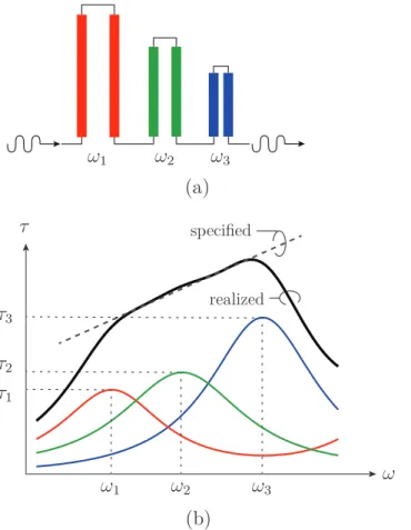
shown in Fig. 2.4(b). This response is periodic in frequency and exhibits delay peaks at λ = (2m + 1)λg/4, where m is an integer. Cascading C-sections of different lengths forms
with group delay responses represented by the colored curves in Fig. 2.4(b) results a total group delay response whose the delay at each frequency is the sum of the delays incurred by each C-section, as represented by the black curve in Fig. 2.4(b).
realized specified τ ω ω1 ω1 ω2 ω2 ω3 ω3 τ1 τ2 τ3 (a) (b)
Figure 2.4 Principles of the C-section phaser. (a) Three Cascaded C-section elements [Fig. 2.3(g)] with different lengths. (b) Group delay response formation for (a). Figure has been reproduced from [1].
While, coupled-resonator phasers [Fig. 2.3(c)], cascaded C-section phasers [Fig. 2.3(g)], and cross-coupled resonator phasers [Fig. 2.3(i)], seem the most promising technologies for ASP systems, artificial (e.g., CRLH) transmission line phasers seem the best option for radiated and spatially dispersive phasers. High-resolution ASP systems require phasers with large dispersion or group delay swings. This issue of phaser characteristics influencing the perfor-mance of an ASP system and the some potential solutions to overcome them are described next.
2.3 Phaser Characteristics and Enhancement
The enhancement of the phaser characteristics increases the performance of the ASP systems. The resolution, the absolute bandwidth, and the magnitude balance are three important phaser characteristics.
The concept of the resolution characteristic can be understood from Fig. 2.1(b), which shows a frequency discriminator as one of the ASP applications. If the group delay difference, ∆τ of the phaser response over the frequencies ω1 and ω2 is not large enough, the pulses will not be
enough discriminated at the output of the phaser. This indicates the resolution of the system is proportional to the group delay difference over center frequencies of the modulated pulses. Moreover, if the pulse duration, T0is reduced, the two output pulse will be well discriminated.
Hence, the resolution of an ASP system ̺, should follow ̺ ∝ ∆τ/T0 or similarly, ̺ ∝ ∆τB0,
where B0 is the bandwidth of the input pulse.
In order to increase the resolution of an ASP system, the group-delay swing of the phaser that it utilizes should be increased. This can be achieved using a brute-force approach by cascading a large number of phasers. This approach leads to an unacceptable high insertion loss preventing signal detection in the presence of the noise. Figure 2.5(a) represents a tech-nique to enhance the ASP resolution by using a feedback loop circuit. In this system, the signal at the output of the phaser, yN(t) is regenerated by an amplifier and re-injected via a
non-dispersive delay line toward its input along a loop. At each pass across the phaser, the effective group delay slope of the system is increased, so that after N turns along the loop the time-frequency resolution has been enhanced by a factor N. So, the resolution has been multiplied by the same factor. Figure 2.5(b) shows the group delay slope of the system which is progressively increased as the signal loops in the system. This technique and its applica-tions will be discussed in Chapter 3. Usage of the feedback technique solves the problem of limited microwave phaser resolution in much more efficient manner.
The required absolute bandwidth and group delay of the phaser vary based on the applica-tions. For instance, the absolute bandwidth of the phaser in frequency sniffer which will be discussed in Chapter 5 is 9 GHz with 3.5 nsec group delay swing. In frequency sniffer appli-cation where the absolute bandwidth is 9 MHz the group delay swing should be much more bigger, so 3.5 nsec group delay may be much more insufficient. In this case, another phaser technology such as reflection-type coupled-resonator [23] must be used. Where the relevant frequency bandwidth is very small in some applications, the absolute frequency bandwidth of the phaser will be an essential figure of merit.
PSfrag x(t) phaser τ(ω) amplifier G τ0 divider delay line yN(t) isolator (a) ω τ 1 2 N ∆ω ∆ τ1 ∆ τN = N ∆ τ1 ×N (b)
Figure 2.5 Loop resolution enhancement principle [2]. (a) Circuit block diagram. (b) Group delay slope (|φ2|) multiplication.
as the flat insertion loss, S21 over the bandwidth of the transmission phaser which is the
characteristic of the ideal phaser as shown in Fig. 2.2. In the real case, the insertion loss of the phaser is not flat due to frequency dependent dielectric and conductor losses. Compared to the total amount of losses, which can be compensated using loop architectures, a non-flat transmission response poses serious difficulties such as signal distortions in ASP techniques. Therefore, transmission phasers require an amplitude equalization network to compensate non-flatness magnitude [28]. We will see how magnitude imbalance comes about, how it affects ASP, and how to remedy it for higher ASP performance in "System Problematic" section.
2.4 Phaser Synthesis
The goal of phaser synthesis is to obtain a response as close as possible to the ideal response shown in Fig. 2.2. So, the phaser resolution must be adequately high, its insertion loss must be flat, and its absolute bandwidth should be convenient for the intended application. The
shape of the phaser response is mostly linear, as required for instance in RTFT and pulse compressors, but it may be quadratic, cubic based on the application. The phaser response can also be more complex as stepped group delay response used in spectrum sniffer to be presented in Chapter 5.
A synthesis of the the C-Sections network phaser has been well presented in the article [3]. In this synthesis, the arbitrary group-delay response is achieved by combining the group-delay responses of C-sections with different lengths. Moreover, a computer design approach based on genetic algorithms is applied in this synthesis, which consists of determining the structural parameters of the different C-section groups.
A systematic synthesis method for cross-coupled phasers with controlled magnitude for ASP applications has been introduced in the article [17]. The transfer function is synthesized using a polynomial expansion approach, which allows to separately control the magnitude and group-delay response of the phaser.
The concept of space mapping has been applied for the first time in the article [27], to design a phaser using coupled C-sections. The results indicate that the space mapping synthesis technique for phaser design is more accurate and the implementation is simple compared to generic algorithms synthesis, presented in [3].
The synthesis of narrowband reflection-type phasers with arbitrary prescribed group delay has been presented in the article [29]. A high group-delay swing at a narrow frequency band is achievable using this technique.
2.5 System Problematic
There is a big demand for high resolution systems in the ASP applications, such as frequency sniffing and real-time FDM modulation [16]. The cascading of the phasers is a common approach for resolution enhancement. However, the resulting system would be large, and would suffer from high insertion loss. Moreover, The system would have a poor signal-to-noise due to the low level of the signal reaching the amplifier in the end of the phaser. One solution may be using a lower loss dielectric and conductor material in phaser design but that increases the overall cost of the phaser. Another solution is loop feedback system which is presented in Chapter 3.
When a broadband pulses are injected to a phaser, the output pulses will be time-spread because of dispersive characteristic of the phaser. The larger pulse bandwidth results a wider pulse in time. So, the resolution of the system is decreased. Chapter 5 presents a stepped group delay pahser design where the a multiple channel input is discriminated in time domain,
where each channel occupies a non-dispersive frequency band.
A phaser has a non-flat insertion loss, based on frequency dependent dielecteric loss, αd∝ ω
and conductor loss, αc ∝ √ω. This non-flat response leads the system to distort the input
signal by an attenuation factor, e−αm(ω)l = e−(αc(ω)+αd(ω))l, where l is effective length of the
phaser. The attenuation factor strongly depends on frequency, and increases with frequency in an up-chirp phaser, and may decrease in some delay desings with frequency in a down-chirp phaser, shown in Fig. 2.6. Once solution to overcome this issue is the equalization of the amplitude by an equalizer circuit with an opposite slope insertion loss [30].
τ τ ω ω |S21| |S21| up-chirp down-chirp τ(ω) αm = αc+ αd ατ α= αm+ ατ (a) (b)
Figure 2.6 Magnitude imbalance due to the loss in a phaser. (a) Material and dispersion losses for an up-chirp phaser. (b) Material and dispersion losses for a down-chirp phaser.
R-ASP system has a lot of applications in the impulse regime. Pulse compressors and stret-chers, pulse radar, UWB systems, and impulse radios are example for R-ASP applications. Also, UWB pulses are the important part of the R-ASP systems in impulse regime. UWB pulse generation technique mostly uses digital and CMOS technique which is expensive and high power consumption. A new low-cost analog technique for UWB pulse generation based on mixing with an auxiliary pulse are presented in Chapter 4.
Finally, a phaser with the millimeter-wave frequency range is highly desired for ultra high speed ASP applications. However, the fabrication limitation and high insertion loss of the conventional phasers at millimeter-wave frequencies limit their usage for millimeter-wave applications. So, more research and development in this area is needed. Since the insertion loss and the spectral bandwidth of the wave guide transmission lines at high frequency are much better than printed circuit boards (PCB) (i.e. microstrip and stripline), they may be good candidates as an alternative technology for future phaser design. Similarly, the coplanar waveguide technology maybe more suitbale for PCB based phaser design.
CHAPTER 3 ARTICLE 1: INCREASED GROUP-DELAY SLOPE LOOP SYSTEM FOR ENHANCED-RESOLUTION ANALOG SIGNAL
PROCESSING
Babak Nikfal, Shulabh Gupta, and Christophe Caloz
IEEE Trans. Microwave Theory Tech., vol. 59, no. 6, pp. 1622-1628, Jun. 2011.
A novel increased group delay slope loop scheme is proposed to enhance the time-frequency resolution of dispersive delay structure (DDS) components for microwave analog signal pro-cessing systems. In this scheme, the signal at the output of the DDS is regenerated by an amplifier and re-injected via a non-dispersive delay line toward its input along a loop. At each pass across the DDS, the effective group delay slope of the system is increased, so that after n turns along the loop the time-frequency resolution has been enhanced by a factor n. This approach provides a solution to the unpractical approach of cascading n DDS units, which would lead to excessively large device footprint, unacceptably high insertion loss and severe signal-to-noise reduction. The proposed scheme is implemented in a proof-of-concept circuit using a C-section all-pass network DDS and demonstrated experimentally in a frequency meter and in a frequency discriminator. Possible improvements for higher performance are discussed.
3.1 Introduction
Temporal (as opposed to spatial) frequency dispersion is the property according to which a material delays the different time spectral components of a modulated signal by different amounts of time [31]. This effect is commonly used at both optical [32] and radio [33] fre-quencies for analog signal processing, i.e. for the real and continuous time manipulation of broadband signals, with particular benefit for low-complexity and high-speed instrumenta-tion and communicainstrumenta-tion systems [34]. Although it has been less applied in microwave compo-nents, mainly due to the difficulty of realizing efficient dispersive delay structures (DDS) in the corresponding frequency range, dispersion engineering has a great potential in this area to address new challenges in faster, higher frequency and more reconfigurable circuits, using various real-time systems, such as frequency meters and discriminators, real-time Fourier transformers, convolvers, correlators and compressive radars [33–35].
Over the past few decades, several microwave technologies have been explored for DDSs, including surface acoustic wave (SAW) [19, 34], magnetostatic wave (MSW) [18, 36],
super-conducting cascaded coupler [37], chirped transmission line [15, 38], metamaterial struc-ture [39, 40] and all-pass network [3, 13] technologies, all exhibiting different merits and drawbacks. SAW, MSW and superconductive technologies are not well amenable to several microwave DDS applications due to restricted maximal frequency, biasing magnet require-ment and cryogenic constraint, respectively. In contrast, more recent chirped transmission lines, metamaterial and all-pass network DDSs are implemented in standard low-cost and frequency-scalable microwave integrated circuit technologies, and they have already led to efficient real-time Fourier transformers [3, 8], tunable pulse delay lines [9], ultra wideband modulators [10] and compressive receivers [11]. However, the performances of these DDS systems are limited by the maximal achievable group delay difference ∆τ over the frequency band of operation ∆f, i.e. the maximal delay difference and frequency difference product, ∆τ × ∆f, which define the time-frequency resolution and bandwidth, respectively, of the system.
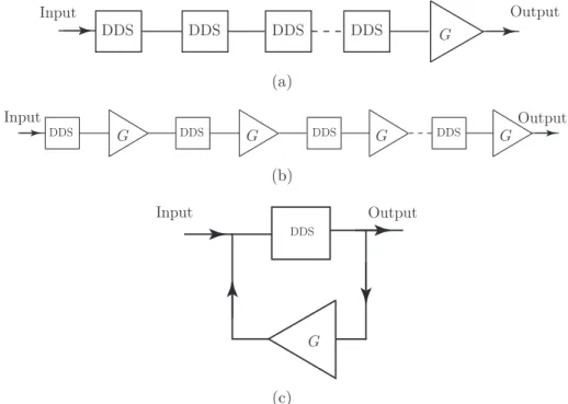
In order to achieve a large ∆τ × ∆f product to maximize the time-frequency resolution of analog signal processors, several approaches can be followed. The simplest technique is to cascade a large number of DDSs, as shown in Fig. 4.1(a), until the required group delay difference has been reached. However, this approach is practically unrealistic as it leads to an excessively large device footprint and to unacceptably high insertion loss, preventing signal detection in the presence of parasitics and noise. The losses in the structure may be conceptually compensated by using an amplifier with a high gain. However, this is an expensive device. Moreover, if the amplifier is placed at the end of the cascade, both the useful and the unwanted parasitic signal are amplified, which makes detection problematic ; if placed at the front of the cascade, the amplifier will typically saturate. In either case, using a high-gain amplifier severely restricts the performance of the system. This requirement for a high gain amplifier may be alleviated by using a distributed amplification scheme, as illustrated in Fig. 4.1(b). This approach relaxes the high gain constraints of the amplifier at the cost of requiring a large number of devices, which in turns leads to high power consumption, high cost and high biasing circuit complexity. In addition, both schemes, in order to provide a total group delay swing of n∆τ, require n DDS units, n amplifiers and n other circuit components such as matching sections and biasing networks, which naturally results in larger size, high system cost and high complexity. Therefore, the cascading approach becomes impractical when a large group delay swing is required.
Compared to these techniques, this paper solves the problem of limited microwave DDS resolution in a much more efficient manner by using a novel DDS loop scheme. The proposed scheme enhances the resolution of any DDS by passing the signal several times across it and regenerating it by amplifying it after each pass, as illustrated in Fig. 4.1(c). The proposed
loop system is compact in size and requires only one set of circuit components, i.e. DDS, amplifier, matching section and biasing network, resulting in lower power consumption and lower system cost, compared to the two aforementioned cascading schemes. In addition, the proposed system is highly flexible in achieving variable amounts of group delay swing by simply controlling the number of turns in the loop (for instance using a switch and a counter), which is not possible in the cascading approach. This makes the system versatile and suitable for various applications requiring different amounts of group delay swings. The paper is organized as follows. Sec. 3.2 describes the principle of the proposed DDS loop system. Sec. 3.3 presents its prototype implementation using a C-section all-pass network as the DDS, and demonstrates two subsequent applications: a frequency meter [41, 42] and a frequency discriminator [43, 44]. Sec. 3.4 discusses possible improvements of these proof-of-concept demonstrations. Finally, conclusions are given in Sec. 3.5.
Input Output G DDS DDS DDS DDS (a) Input Output G G G G DDS DDS DDS DDS (b) Input Output G DDS (c)
Figure 3.1 Different possible techniques for increasing the group delay swing of a dispersive delay structure (DDS). (a) Cascaded DDSs with a single amplifier. (b) Cascaded DDSs with distributed amplification. c) Proposed loop technique.
3.2 Principle
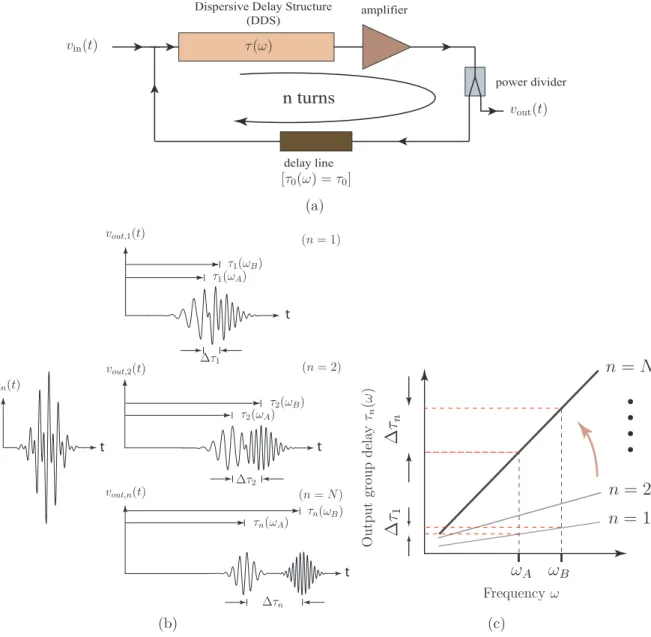
Fig. 3.2(a) shows a simplified schematic of the system, which essentially consists of a loop, placed between the input and output ports and including a DDS with a group delay response
τ(ω), an amplifier, a frequency-independent (non-dispersive) delay line of delay τ0 and a
power divider.
Dispersive Delay Structure (DDS) power divider amplifier delay line n turns [τ0(ω) = τ0] vin(t) vout(t) τ(ω) (a) t t t t ∆τ1 ∆τ2 ∆τn τ1(ωB) τ1(ωA) τ2(ωB) τ2(ωA) τn(ωB) τn(ωA) vin(t) vout,1(t) vout,2(t) vout,n(t) (n = 1) (n = 2) (n = N) (b) Frequency ω ωA ωB ∆ τ1 ∆ τn n= 1 n = 2 n = N O ut pu t gr ou p de la y τn (ω ) (c)
Figure 3.2 Principle of the proposed increased group delay slope system. (a) Schematic. (b) Illustration of enhanced time resolution with increased number of turns for the case of an in-put gaussian pulse modulated with two carrier frequencies ωAand ωB. (c) Slope enhancement,
providing an n-fold increased resolution [sn in (3.2)] for analog signal processors.
The essential function of the loop is to enhance the group delay difference in a given frequency range from the amount provided by the single DDS, ∆τ, to n × ∆τ, by passing the input signal n times into the DDS. This group delay enhancement subsequently increases, by the same factor n, the real-time frequency resolution of analog signal processors.
Let us consider an input signal vin(t) constituted by a single pulse v0(t) modulated with two
carrier frequencies ωA and ωB, respectively, i.e. vin(t) = vin,A(t) + vin,B(t) = v0(t) sin(ωAt) +
v0(t) sin(ωBt).
First, vin(t) is injected into the loop. At the first pass across the DDS (n = 1), the A and
B spectral components of the signal, due to their different group delays incurred by the DDS, are separated in time by the amount ∆τ1 = τ(ωB) − τ(ωA) within the frequency range
[ωA, ωB], as shown in Fig. 3.2(b). The amplifier compensates for the losses introduced by the
DDS and by the other elements of the loop. The resulting signal, with time separated pulses, is then split by a power divider. Part of it becomes the first pulse vout,1(t) of the output signal,
vout(t), while the other part is re-injected toward the input of the DDS via the non-dispersive
delay line. After the second pass across the DDS (n = 2), the time separation between the A and B components of the signal is doubled, i.e. ∆τ2 = 2∆τ1, as shown in Fig. 3.2(b). This is
the same thing as saying that the group delay slope of the system, or equivalent group delay slope, has doubled, within the same frequency range.
Thus, the effective ∆τ × ∆f product of the system has doubled. As before, the amplified signal, with its A and B components now twice further apart in time, is split by the power divider to build for one part vout,2 and to be for the other part re-injected into the system.
And the cycle continues, so that after n turns around the loop, the A and B components of the input signal have been resolved in the output signal vout,n by a time separation of
∆τn= n∆τ1, as shown in Fig. 3.2(b).
The ∆τ × ∆f product has thus increased by a factor n. The explanation just given for a two-tone modulation can be straightforwardly extended to the case of a broadband signal including a continuum of frequencies across the bandwidth of the DDS, for which the system can operate as a real-time Fourier transformer if sufficient dispersion is available [13, 15]. The role of the non-dispersive delay line is to avoid self-overlapping of the pulse traveling around the loop, i.e. the superposition of its trailing part entering the DDS and of its leading part exiting the DDS. To avoid such overlap, the condition ∆ℓ/vg >∆T must be satisfied,
where ∆ℓ is the length of the DDS, ∆T is the time duration of the pulse and vg is the
group velocity the DDS. As this condition is generally not satisfied from the DDS only, the additional delay τ0 of the non-dispersive delay line is used to provide the overlap avoidance
condition ∆ℓ/vg + τ0 >∆T . In practice, a slightly larger τ0 value is required to take into
account the time spreading effects due to dispersion. The additional delays due to the other components of the loop (e.g. amplifier and matching elements) may be absorbed in the delay τ0.
τn(ω) = nτ(ω) + (n − 1)τ0, (3.1)
which corresponds to the group delay versus frequency slope
sn =
dτn(ω)
dω = n dτ(ω)
dω = ns1, (3.2)
where s1 corresponds to the slope of the isolated DDS. As will be seen later, sn is the
time-frequency resolution of the system, i.e. its frequency resolution obtained from the time domain.
At this stage, it is important to differentiate the proposed loop system from a conventional feedback system operated in the continuous wave regime. In contrast to such a system, the proposed loop system operates in the impulse regime. Due to this regime, the traveling pulsed signal never overlaps with itself. The presence of the delay element of constant delay τ0 in the
loop ensures this condition by delaying the pulse enough so as to avoid any overlap between its leading and trailing edges. Maintaining in addition the loop gain always smaller than unity within the operation frequency band of the DDS, thereby avoiding the Barkhausen oscillation criterion [45], ensures the stability of the system. In practice, the loop system could potentially oscillate due to parasitic signals outside the frequency band of operation. However, this issue can be easily avoided by placing a bandpass filter in the loop. In this case, the DDS must be co-designed with the filter and specifically take into account its group delay response, in particular near the cutoff frequencies, which can be systematically achieved by using non-commensurate all-pass networks [3].
3.3 Experimental Demonstration 3.3.1 C-Section Implementation
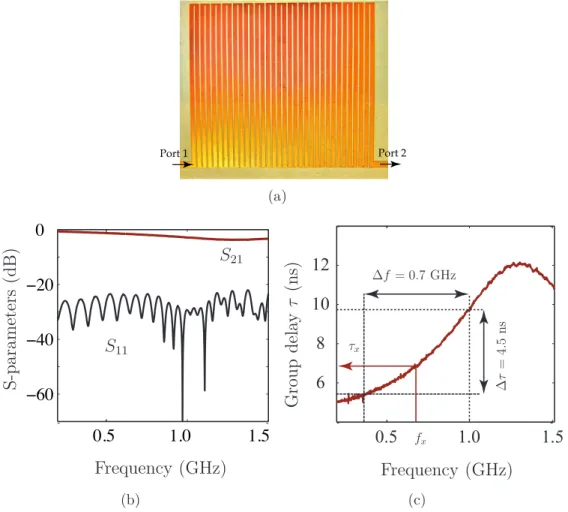
For the sake of illustration of the proposed increased group delay slope system, we shall consider an implementation using a C-section network as the DDS [3]. This DDS is a planar version of the all-pass filter [30, 46] introduced by Hewitt in [47], and extended in [3] for the systematic design of quasi arbitrary group delay responses. Fig. 3.3 presents the measured response for a commensurate (all C-sections with same length) microstrip C-section all-pass network, which will be used in the system prototype shown in Fig. 3.4(a). Non-commensurate C-section networks with other desired group delay profiles and slope signs [3] could have been chosen. Fig. 3.3(b) shows the S-parameters while Fig. 3.3(c) shows the group delay response of the DDS. The length of the C-section network has been restricted so as to avoid excessive
insertion loss and mismatch while still providing a substantial time-frequency resolution, here ∆τ = 4.5 ns within the 0.3-1.0 GHz frequency range.
Port 1 Port 2 (a) 0.5 1.0 1.5 −60 −40 −20 0 Frequency (GHz) S-pa ra m et er s (d B ) S11 S21 (b) 6 8 10 12 0.5 1.0 1.5 G ro up de la y τ (n s) Frequency (GHz) ∆ τ = 4. 5 ns ∆f = 0.7 GHz τx fx (c)
Figure 3.3 Microstrip C-section all-pass network used as the dispersive delay line in the system shown in Fig. 3.2(a). a) Photograph of the C-section structure. b) Measured S-parameters and c) Group delay τ(ω).
3.3.2 Loop System Implementation
The complete system prototype is shown in Fig. 3.4(a) while its schematic, showing the va-rious components along with the biasing networks and capacitors for DC and low-frequency isolation, is represented in Fig. 3.4(b). The corresponding experimental setup is shown in Fig. 3.4(c). The prototype consists of an RF mixer (ADE-42MH from Minicircuits) which modulates a time-domain Gaussian pulse (with fixed width in all forthcoming experiments), generated by an arbitrary pulse generator, with an input signal fLO. This produces the
with 50 Ω input and output impedance) is placed just before the mixer as a precaution to minimize any reflection that may occur in case the input impedance of the RF mixer deviates from 50 Ω. Another attenuator (3-dB) is placed at the output of the mixer to reduce signal transmission toward the input port through the mixer due to possible mismatch in the loop circuit. The signal vin(t) enters the loop and passes through the DDS. The DDS output is
then amplified by using an MMIC amplifier (ERA-5 from Minicircuits) to compensate for the loss experienced by the signal. A part of this amplified signal is extracted using a power divider (ADP-2-10 from Minicircuits), which is fed to an oscilloscope for monitoring the si-gnal in the loop for each turn. The rest of the amplified sisi-gnal is maintained in the loop and passed through a coaxial cable (external to the board here) exhibiting a constant group delay τ0 (non-dispersive). The delayed signal passes then through another attenuator (3 dB) in the
loop. This attenuator acts as an isolation device between the junction impedance Z1 (ideally
25 Ω) and Z2 = 50 Ω, as indicated in the schematic of Fig. 3.4(b). The attenuators were used
here as a simple and low-cost solution for handling mismatches in the proof-of-concept pro-totype. A straightforward higher-performance but higher-cost approach would be to replace the attenuators by an isolator (with 50 Ω input and high output impedance) placed after the mixer to achieve Z1 = 50 Ω.
3.3.3 Calibration
Before operation, the loop system must be calibrated to account for the effect of multiple turns and for the effect of the delay τ0 induced by the non-dispersive delay line and the other
loop elements. The calibration consists essentially in determining τ0, which may take different
values corresponding to different cable lengths or electronically tuned electric loop lengths for the measurement or processing of different signals. In a fixed loop system, for instance integrated on a chip and accomplishing a pre-determined function, τ0 would be invariable and
could therefore be predetermined at the circuit design stage, so that the calibration presented here could be skipped.
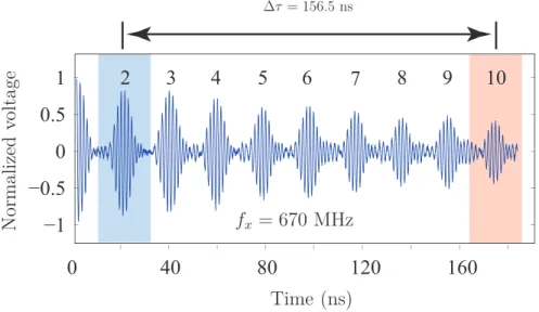
In order to perform calibration, a modulated pulse vin(t) = v0(t) sin(ωxt), with a known
modulation frequency ωx within the range of the used DDS, is injected into the system. The
corresponding output signal vout(t), measured by an oscilloscope, is shown in Fig. 3.5 for
a typical modulated signal. According to (3.1), the time difference between nx + 1 peak
maxima in vout(t) is
dispersive delay Structure (DDS) MMIC amplifier mixer power divider B: signal generator C: oscilloscope D: coaxial cable constant delay A: gaussian pulse E: loop system attenuator vin(t) v0(t) vout(t) fLO τ0 (a) v0(t) vout(t) attenuator fLO DDS τ0 G power divider Vcc RFC mixer Z2= 50 Ω Z1 50 Ω 50 Ω (b)
A
B
C
E
D
(c)Figure 3.4 Experiments. a) System prototype, corresponding to Fig. 3.2(a), and incorporating the DDS of Fig. 3.3. b) Schematic. c) experimental setup, with corresponding A, B, C, D and E labels between (a) and (b). Only the major components are indicated.
where τx = τ(ωx) and ∆τx,n = ∆τn(ωx) = τn+k(ωx) − τk(ωx), k being an arbitrary integer
and nx being chosen large enough to allow accurate time resolution. From this equation, we
obtain
τ0 =
∆τx,n− nxτx
nx− 1
. (3.4)
Since τx is available from the known group delay response of the DDS, which is given in
Fig. 3.3(c) in the case of the presently considered C-section DDS, the terms of this expression are all determined. Therefore, τ0, which is a constant under the assumption that the elements
of the loop other than the DDS exhibit negligible dispersion within the operation bandwidth, has been determined. This completes the calibration procedure. The calibration data for the signal in Fig. 3.5 are given in the caption of the same figure.
2 3 4 5 6 7 8 9 0 40 80 120 160 −1 −0.5 0 0.5 1 10 Time (ns) fx = 670 MHz N or m al iz ed vo lt ag e ∆τ = 156.5 ns
Figure 3.5 Calibration (measured) time-domain output signal [vout(t)] for an input pulse
[vin(t)] modulated by a known frequency ωx using the circuit prototype and experimental
setup of Fig. 3.4. The results used here in connection with (3.4) are fx = 670 GHz,
corres-ponding according to Fig. 3.3(c) (or a more accurate DDS loop-up table) to τ(ωx) = 6.95 ns,
and n = 8 with k = 2, leading to τ0 = 14.42 ns.
3.3.4 Frequency Meter Application and Results
The frequency meter application is straightforward once τ0 had been determined following
the calibration procedure described in the previous section.
This time, the center (or modulation) frequency of the input signal vin(t) is unknown and
![Figure 2.1 Essential effects in ASP. (a) Chirping. (b) Frequency discrimination. Figure has been reproduced from [1].](https://thumb-eu.123doks.com/thumbv2/123doknet/2341930.34051/25.918.210.714.100.580/figure-essential-effects-chirping-frequency-discrimination-figure-reproduced.webp)
![Figure 2.2 An arbitrary group delay with flat lossless magnitude response. Figure has been reproduced from [1]](https://thumb-eu.123doks.com/thumbv2/123doknet/2341930.34051/26.918.288.631.103.417/figure-arbitrary-group-lossless-magnitude-response-figure-reproduced.webp)
![Figure 2.5 Loop resolution enhancement principle [2]. (a) Circuit block diagram. (b) Group delay slope (|φ 2 |) multiplication.](https://thumb-eu.123doks.com/thumbv2/123doknet/2341930.34051/31.918.239.692.104.577/figure-resolution-enhancement-principle-circuit-diagram-group-multiplication.webp)