ELECTRODEPOSITION AND CHARACTERIZATION OF ZnO THIN FILMS
FOR SOLAR CELL APPLICATIONS
RU LI
DÉPARTEMENT DE GÉNIE CHIMIQUE ÉCOLE POLYTECHNIQUE DE MONTRÉAL
MÉMOIRE PRÉSENTÉ EN VUE DE L’OBTENTION DU DIPLÔME DE MAÎTRISE ÈS SCIENCES APPLIQUÉES
(GÉNIE METALLURGIQUE) MARS 2011
UNIVERSITÉ DE MONTRÉAL
ÉCOLE POLYTECHNIQUE DE MONTRÉAL
Ce mémoire intitulé:
ELECTRODEPOSITION AND CHARACTERIZATION OF ZnO THIN FILMS
FOR SOLAR CELL APPLICATIONS
Présentée par : LI RU
en vue de l’obtention du diplôme de : Maîtrise ès sciences appliquées a été dûment accepté par le jury d’examen constitué de :
M. AJERSCH FRANK , Ph.D., président
M. SAVADOGO OUMAROU, D.d’état, membre et directeur de recherche Mme. BRISARD GESSIE, Ph.D., membre
ACKNOWLEDGEMENTS
“No pain, no gain.” This old saying has been my motto for decades — it not only has mentally prepared me for higher education but also renews my faith from time to time. In addition to my motto, my graduate study years at École Polytechnique de Montréal have been crucial to my scholarly accomplishment. This distinguished school’s first-class academic atmosphere and excellent up-to-date technology has trained me well for my future career.
My thesis would not have been possible without the people who helped me with their precious time and valuable assistance. Thus, I would like to take this opportunity to thank those who had a great influence on me, and those who contributed to this thesis.
First of all, I am honoured to have been studying under the guidance of Dr. Oumaro Savadogo. It is his vision and continuous support that has made me a tougher and more knowledgeable scientist. While at different phases of my thesis research, extensive discussion with Dr. Savadogo allowed me to form a proper methodology with the most practical measurement instruments.
Secondly, I am also indebted to Dr. Christopher W. Bale, Dr. Cevdet Akyel, and Prof. Huguette Mallet. I am very grateful to their patience when learning great theoretical and operational skills from them through all kinds of different means of communication. Their support and knowledge were very helpful during my research project.
Thirdly, special thanks to all technicians and employees of the CM2 especially Éric Duchesne (SEM), Jean-Philippe Masse (XRD), Mathieu Boisvert (SEM), Philippe
Plamondon, and Philippe Beaulieu (SEM). The training and guidance that I gained from them are much appreciated.
Fourthly, I also wish to thank my colleagues who have supported me in the laboratories: Kentaro Oishi, Stéphane Leveguo, Huiming. Thank you for your help in discussing the probabilities and in preparing for my experiments to run smoothly.
Last but not the least; I would like to extend my gratitude to our technician Carole Massicotle and Delisle Robert. Thank you for keeping the raw materials organized, for keeping our models in working order, and for getting in touch with our suppliers when needed. Without you, I could not have started or finished in the desired time.
This thesis is also a gift dedicated to my daughter and my parents. Their unconditional support has kept me going this far. Thank you!
RÉSUMÉ
Ce travail porte sur l’étude de la composition chimique, la morphologie et les propriétés optiques des couches minces d’oxyde de zinc déposées par voie électrochimique à partir d'une simple solution aqueuse de chlorure de zinc. Les rangées de nanotiges de ZnO ont été préparées et déposées sur un substrat de dioxyde d’étain dopé au fluor (FTO) à basse température. Les images des nanostructures obtenues par la microscopie électronique à balayage ont montré une structure wurtzite, ou des grains hexagonaux de forme semblable à une tige (aiguille) perpendiculaires à la surface du substrat. Et la couche mince possède une épaisseur d'environ 0.4 - 2.11µm.
Le spectre de diffraction par rayon-X montre que la composition chimique des couches minces est presque pure et l’orientation préférentielle de la croissance de ZnO est (002), cette direction est bien est en accord avec les résultats obtenus dans la littérature par calcul. Il est admis que les oxydes métalliques obtenus à l’échelle nanométrique qui conduisent à une distribution ordonnée des charges sont soit de forts accepteurs d’électrons ou favorisent le transport de charges à partir des canaux continus formés le long des nanotiges. Par exemple, ces matériaux possèdent des affinités et des mobilités électroniques élevées qui permettent d’améliorer les propriétés électriques de la photoanode dans une pile solaire photosensibilisée car ceci favorise le transport de charge issu du canal continu le long des nanotiges.
La mesure des propriétés électriques, notamment la mesure de la résistivité a été effectuée par la méthode des quatre points. À travers la mesure et le calcul, le résultat des résistivités est d'environ 4.39×10³ Ωcm-1, pendant que les énergies de la bande interdite, calculées à
partir des résultats expérimentaux par la méthode graphique, sont comprises entre 3.5~3.7eV les échantillons préparés avec des concentrations de 5 mM en inos Zn2+
En outre, dans la présente recherche, nous avons élaboré et optimisé une méthode de formation des couches minces de nanotiges de ZnO par électrodéposition à basse température sur cdes substrats de verre conducteurs. L'épaisseur effective de la couche mince est d’environ 2.11µm, ce qui est évidemment un facteur qui affecte la conductivité et le taux de transport électronique, ainsi que sur la recombinaison liée à la distance parcourue par les porteurs de charge. Ce document présente également les résultats sur les conditions expérimentales optimisées sur la concentration des espèces électroactives utilisées, la température et les paramètres électrochimiques (potentiel et densités de courant) d’élaboration des couches de ZnO les plus performants pour des applicationsdans les dispositifs solaires, la méthode d’électrodéposition utilisée est pratique, efficace et fait gagner du temps. Sur la base des meilleures caractéristiques physico-chimiques obtenues des différentes couches de ZnO qui ont été élaborées, il a été conclu que les électrodes fabriquées à 650C, pendant 40 minutes avec une concentration d'électrolyte de 5mM de chlorure de zinc et 0.1M de chlorure de potassium pour soutenir la solution et un potentiel de dépôt de -1 V/ECS sont les plus performantes. Il a été aussi conclu que les meilleures conditions de l’électrodéposition des électrodes ZnO ont été déterminées. Les résultats peuvent être utilisés dans des travaux ultérieurs pour développer des systèmes énergétiques solaires basés sur des nanotiges de l’oxyde de zinc.
Il a été montré que la composition chimique de l’électrolyte de d.épost est crutiale pour la formation de des nanostructures de ZnO ayant des morphologies bien définies. Des structures de type Wurzite avec des nanostructures d’orientation cristallographique préférentielle (002). Les nano tiges de ZnO sont perpendiculaires à la surface du substrat de
verre conducteur. Nos résultats expérimentaux doivent supporter l’idée que le mécanisme probable de’électrodéposition de ZnO implique un processus de dissolution précipitation qui qui implique l’oxygène comme précurseur. Ceci se traduit par les équations suivantes :
O2 + 2H2O + 4e → 4OH- Zn 2+ + 2 OH- → Zn (OH)2 Zn(OH)2 → ZnO +H2O
Ce comporte des étapes d’adsorption de l’ion hydroxyde, la précipitation de l’hydroxyde de zinc et la déposition de l’oxyde de zinc . Les facteurs qui déterminent la morphologie doivent être déterminées de façon précise par des études futuresLes couches de film de ZnO obtenu ont des valeurs de résistivité typique de 10-3 à 105 Ωcm-1. La valeur de la largeur de la bande interdite obtenue à partie des mesures de transmit tance optique des échantillons ont montré une valeur qui varie entre 2.95~3.7eV. Ce sont des valeurs qui sont adaptées à l’utilisation de ce matériau pour des applications solaires. . Ceci permettra une meilleure compréhension des propréts de ce matériau selon les domaines d’applications.
ABSTRACT
In this work, we investigated the chemical composition, morphology and optical properties of zinc oxide thin films deposited from a simple aqueous zinc chloride solution. The ZnO nanorod arrays were prepared and grown on fluorine doped tin dioxide (FTO) substrate at low temperature. The nanostructure images obtained by scanning electron microscopy showed that it had the wurtzite structure or hexagonal grains with rod (needle) like shape perpendicular to the substrate surface. The X- ray diffraction patterns indicated that the thin films were almost pure. The preferential orientation of ZnO growth was (002), a direction that matched calculation. These nanoscale metal oxides having ordered distributions are strong electron acceptors with high electron affinity and electron mobility which improves the electric property of photoanode and charge transport due to continuous channeling along the nanorods.
In this present research, we additionally developed and optimized a method electrodeposition at low temperature for forming thin films comprising ZnO nanorods used as photoanode. The effective thickness of the thin film was about 2.11µm, which is obviously a factor affecting the conductivity and electron transport rate, as well as recombination related to the carriers transport distance. This workalso shows clearly that that the electrodeposition method is practical, effective and time saving: the experiments were carried out at 650C over 40 minutes with electrolyte concentrations of 5mM zinc chloride and 0.1M potassium chloride support solution. It was also concluded that the best conditions of the electro deposition of the ZnO electrodes were determined. The results can
be used in further work to develop for examples solar cells devices based on ZnO nanowires.
The X-ray diffraction pattern and EDX information obtained from the Philips-X’pert and JEOL 840A instruments revealed the characteristics of the ZnO thin film composition. They indicated that this film is made of polycrystalline of the ZnO
EDX semi-quantitative analysis showed bright particles and dark particles which respectively represent ZnO nanorods and base background (Also see Table 2). In the 5mM ZnCl2 electrolyte concentration group, the thin film evidently covered the substrate very well since smaller relative amounts of Sn and Si were detected on the top of the films while the other two groups of 1mM and 0.5 mM were obviously worse. This phenomenon might be interpreted by EDX resolution. It is known that EDS can identify a spot size of a few microns of samples, it detected a small amount of Sn and Si coming from the coated glass substrate (SnO layer) during detector is collecting the characteristic X-ray of Sn and Si elements into an energy spectrum. It is very important is that films of ZnO are of good quality one because these impurities, such as Cl- or other elements cause defects in the thin films (The ohmicity of the contact between substrate and deposited thin film is good when there is no any aid of detects in growth proceeding).
Another important parameter is the understanding of the mechanisms and electrochemical behavior of the complex ions in solution which is still not very well understood. Our results may support the common view which involves a precipitation-dissolution process. When oxygen is present as precursor, ZnO electrodeposition would comply with the following equations:
O2 + 2H2O + 4e → 4OH- Zn 2+ + 2 OH- → Zn (OH)2
Zn(OH)2 → ZnO +H2O
The equations indicate three main steps: the adsorption of hydroxide ion, the precipitation of zinc hydroxide and the deposition of ZnO. Despite these assumptions, for the time being, the mechanisms and factors that govern the morphology of the ZnO produced need more studied to be carried out for a better understanding of the process
The composition of the electrodeposition solution is crucial for the formation of ZnO nanostrucutres with well-defined morphologies. We obtained the Wurzite structure for ZnO with high purity and rod-shaped nanostructure with (002) preferred crystallographic orientation. The upstanding nanorods are slightly tilted from perpendicular to the glass substrates.
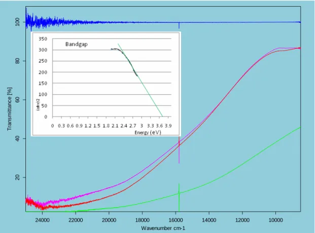
As we know that the resistivity is a key property because it directly and significantly affects electron transport and mobile properties. The films we obtained exhibit typical values over the range 10-3 ~ 105 Ωcm-1. The deduced bandgap energy distributed range from 2.95~3.7eV. These various values of properties of the ZnO thin films are in the range of values very well suitable for solar cell applications.
TABLE OF CONTENTS
ACKNOLEDGEMENTS………iii RÉSUMÉ...v ABSTRACT...viii TABLE OF CONTENTS...xi LIST OF TABLE………..xiii LIST OF FIGURES………...xivLIST OF SYMBOLS AND ABBREVIATION………xvi
CHAPTER 1 INTRODUCTION...1
CHAPTER 2 LITERATURE REVIEWS...6
2.1 Characterized of ZnO Stable Structure and Growth Features………6
2.2 Operational Principle of DSSCs……….7
2.3 Advantages and Disadvantages of Dye-Sensitized Solar Cells………....9
2.4 Pros and Cons of Promising ZnO………...9
2.5 Parameters of Photochemical Characteristics in DSSC………..10
2.6 Choice of Substrate and Dye Materials in DSSCs………...11
2.7 Development ZnO Thin Films by Diverse Means………13
2.8 Development of Composited TiO2/ZnO Electrode………..16
CHAPTER 3 EXPERIMENT………19
3.1 Chemicals and Electrodeposition……….19
3.2 Chemical Characterization………...20
3.3 SEM Characterization………..23
3.5 IR Spectroscope………25
CHAPTER 4 RESULTS AND DISCUSSION………..27
4.1 Chemical Composition of the ZnO Thin film………..28
4.2 Nanostructure of ZnO Thin film………..35
4.2.1 Influence of the Electrolyte Bath Temperature……….44
4.2.2 Oxygen and Zinc Ion Concentration……….44
4.2.3 Influence of the Other Ions in the Electrolyte………...46
4.2.4 Deposition Time………47
4.2.5 Coverage by the Zinc Oxide Film……….48
4.2.6 Orientation……….48
4.3 Resistance……….49
4.4 Optical Properties……….53
4.4.1 Transmittance of ZnO Thin Films……….53
4.4.2 Band gap Values of ZnO Thin Films……….54
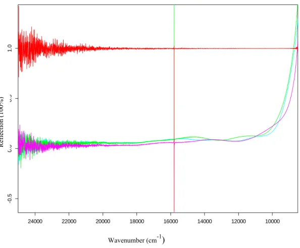
4.4.3 Feflection………...58
4.5 Summary………...59
CHAPTER 5 CONCLUSIONS………..62
CHAPTER 6 FUTURE DIRECTIONS………..64
REFERENCE………...66
APPENDIX………72
LIST OF TABLE
Table 1: Characteristics of Peaks of Thin Films by Electrodeposition from a 5mM ZnCl2 Solution………...32 Table 2: Semi-Quantitative Analysis of Chemical Composition of ZnO Thin Film by EDX…...34 Table 3: Resistivity of ZnO Thin Films………..52 Table 4: Optical Properties of ZnO Thin Films………..59
LIST OF FIGURES
Figure 1: Curves of research year vs. efficiency.The sfficiencies obtained for various materials
and technologies are shown...3
Figure 2: The stable wurtzite of zinc oxide: cubic lattice structure and the zinc znd oxide centers are tetrahedral………...7
Figure 3: Schematic of a liquid electrolyte dye-sensitized solar cell………...8
Figure 4: Chemical structures of K8 and K9 complexes………12
Figure 5: Chemical structures of N3, N719 and K19……….12
Figure 6: Reflection planes in a cubic lattice………..22
Figure 7:Interference spectrum of Bragg’s law……….23
Figure 8: Principle of SEM……….24
Figure 9: Effect of concentration of ZnCl2 (potential/pH diagrams) at 65oC……….27
Figure 10: XRD diagrams. a) 5mM ZnCl2+0.1M KCl at potential: -1.0V, deposition time: 20min. b) 5mM ZnCl+0.1M KCl at potential: -1.0V. deposition time: 40 min. c) 5mM ZnCl+0.1M KCl at potential: -1.0V, deposition time:60 min………31
Figure 11: Patterns from scanning electron microscope with EDX analysis……….33
Figure 12: SEM top view images of ZnO FILMS FROM 5mM group. Top one: 5mM+20 min Middle one: 5mM+40 min, Bottom one: 5mM+60 min……….36
Figure 13: SEM image at 50K magnification from 5mM+40 min and voltage: -1.0V…………..38
Figure 14: SEM cross-sectional image of ZnO film from 5mM+40min, deposition voltage: -1.0V ………39
Figure 15: SEM images of measurement of nanorods size in 5mM and 1Mm system a) 5mM+20min, b)1mM+20min(base length: 249nm, diameter:96.8nm on base), c) 1mM+40min ………39
Figure 16: SEM cross-sectional imaged of measurement of thin film thickness a) and b) 5mM+60min, c) 1mM+20min………41
Figure 18: SEM top view images at constant deposition time and deposition time………..43 Figure 19: Hall mobility as a function of the temperature for a ZnO layer………51 Figure 20: Optical transmittance spectrums of ZnO thin films………..54 Figure 21: Simplified diagrm of the electronic band structure of metals, semiconductors and insulators………55 Figure 22: Reflection diagram of ZnO films………..58 Figure 23: Schematic of process of nuclei formation and growth………..61
LIST OF SYMBOLS AND ABREVIATIONS
A Cross-sectional areaAAM Anodic aluminum oxide membrane
Aλ Absorptance of incident light at specified wavelength CIGS Copper indium gallium selenide
CVD Chemical vapor deposition DSSCs Dye-sensitized solar cells DSC Dye-sensitized solar cell ETA Extremely thin absorber Eg Optical energy bandgap FTO Fluorine-doped tin oxide ITO Indium tin oxide
K Exciton coefficient
K8 dye 4, 4′-bis (carboxyvinyl)-2, 2′-bipyridine ligand (L) as its ruthenium complex [Ru (II) L2 (NCS) 2]
L The length in direction of current flow MBE Molecular beam epitaxy
MOCVD Metal-organic chemical vapor deposition MPN 3-methoxypropionitile
N Density of free electrons
N3 dye cis-bis (2, 2΄-bipyridyl-4, 4΄-dicarboxylato) dithiocyanatoruthenium(II) N719 dye di-tetrabutyl ammonium cis-bis(isothiocyanato)bis(2, 2΄-bipyridyl-4, 4΄- dicarboxylato) ruthenium(II)
P Density of free holes PLD Pulsed laser deposition
PVDF-HFP Poly vinylidenefluoride-co-hexafluoropropylene T Absolute temperature
Tλ Transmittance of incident light at specified wavelength TB Tetrabromophenol blue
TCO Transparent conducting oxide TEP Thermal evaporation process un Electrons mobility
up Hole mobility VLS Vapor-liquid-solid VS Vapor-solid
Z-907dye cis-bis(isothiocyanato)(2,bipyridyl-4,4’-dicarboxylato)(4, 4’-dinonyl-2, 2’-bipyridyl) ruthenium(II)
α Absorbance coefficient
ε Dielectric constant of the semiconductor κ Boltzmann’s constant
σ Conductivity in a solid
λ0 Wavelength of Intrinsic light absorption hυ Photon energy
CHAPTER 1 INTRODUCTION
Solar cells are three categories that include monocrystalline solar cells, polycrystalline solar cells and thin film solar cells. While dye-sensitized solar cells are belong to the group of thin film solar cells.
Based on the photo electrochemical cell concept and development, Michael Grätzel et al introduced an improved dye-sensitized solar cell (DSSC or DSC) in 1991[1]. It has three primary parts: a titanium dioxide thin layer photo-anode, a photosensitive rutheniumpolypyridine dye electrolyte and a platinum metal photocathode. Its conversion efficiency was about 11 percent.
From 1995 to 1999, researchers mainly focus on developing and improving usage of dyes. Circa1955, black dyes were used in DSSCs which each have an efficiency (chance to convert a photon into an electron) of around 80%. More recent dyes achieve almost perfect conversion. Over the last decade, extensive studies have shown that the dyes breakdown under high light intensity.
DSSCs are still at the start of their development cycle. In 2003, it was reported that their thermostabilities increased by using amphiphilic ruthenium sensitizer in conjunction with a quasi-solid-state gel electrolyte. The stability of the device matched that of a conventional inorganic silicon based solar cell. Dye Z-907 and quasi-solid-state gel electrolyte with a 3-MPN-based liquid electrolyte that was solidified by a photo-chemically stable fluorine polymer, PVDF-HFP were prepared in that period. Use of the amphiphilic Z-907 dye in DSC has achieved an energy conversion efficiency of 6.1%. The first solid-hybrid dye-sensitized solar cells were successfully born in 2006. These had alternative semiconductor
morphologies, i.e. arrays of nanowires and a combination of nanowires and nanoparticles, which provide a direct path to the electrode via the semiconductor conduction band. However, their performance is currently limited. The other excellent thermal stability of the 1-ethyl-3-methylimidazolium tetracyanoborate solar cell has proved and exhibited high conversion efficiency for a liquid electrolyte. In 2007, a wide variety of organic dyes based on porphyrin were explored, providing a cell efficiency of about 5.6%. In 2008, Michael Grätzel and colleagues at the Chinese Academy of Sciences fabricated the cell with a new solvent-free liquid redox electrolyte, which consisted of a melt of three salts. The cell efficiency was 8.2%. In 2009, a group of researchers increased the effective surface area of DSSCs by wrapping the cells around a quartz optical fiber. The researchers removed the cladding from optical fibers, grew zinc oxide nanowires along the surface, treated them with dye molecules, and surrounded the fibers by an electrolyte and metal film that carried electrons off the fibers. The cells were six times more efficient than a zinc oxide cell with the same surface area. In 2010, researchers overcame two of the DSC’s major issues, which is to say, created a transparent and noncorrosive electrolyte and a new way to replace the platinum by cobalt sulphide in the cathode. These changes greatly improved the cell’s output and stability.
Fig. 1 summarizes the status of research on solar cells and cell’s efficiencies. The highest efficiencies have been achieved for solar cells with multi-junction concentrators. Thin film solar cells technology consists of a thin layer of photo-electrically active materials deposited between thin conductive films which serve as electrodes on a glass substrate. Cu (In,Ga)Se2 is the best of the thin film materials. These CIGS films have been grown on substrates by physical vapor deposition in a three-stage co-evaporation process.
As indicated above, dye-sensitized solar cells (DSCs) are promising devices for efficient, stable, inexpensive and large-scale solar energy conversion. At the heart of the DSSC system is a mesoporous oxide layer attached to the photoactive electrode,
Fig.1 Curves of research year vs. efficiency. The efficiencies obtained for various materials and technologies are shown. (Source: http://en.wikipedia.org/wiki/Solar_cell)
which providing a large surface area for the absorption of light-harvesting molecules. TiO2 based electrodes are currently used in dye-sensitized solar cells. However, the film based on TiO2 nanoparticles provides a relatively slow electron-transport rate, resulting from the multiple trapping/de-trapping events occurring at the grain boundaries.[2] The new concept for a device includes choice of nanocrystalline materials and optimized method for fabricating the nanostructure of the conducting films. Accordingly there is a need of develop other oxides with appropriate properties for this applications These kind of
materials, the substituted and modified nanostructure of TiO2 film, with relevant value of wide band gap as part of electrode could be ZnO has rendered vast new opportunities for this system.
Many studies have addressed the interpretation of the mechanism of charge transport in nanostructured electrodes. One commonly held view is 1.) transport is mainly diffusion-controlled mechanism with a one-dimensional concentration gradient of electrons normal to conducting substrate mainly drive electrons and 2.) trapping/de-trapping of electrons may be the main cause of the slow transport. A very important parameter for charge transport in photo-anodes is also their morphology.[3] Devices based on interpenetrating networks of mesoscopic semiconductors have shown strikingly high conversion efficiencies. Therefore, the main goal of the research reported here is to synthesize, by electrodeposition method in low temperature, structures having a higher degree of order than a random assembly of nanoparticles. That to say, the desired and functional morphology of films would have the conducting channels aligned in parallel to each other and vertically with respect to the TCO glass current collector. Accordingly, it is very important to develop appropriate ZnO based electrode and well characterized for these applications.
Objectives of this study
The main objective of this work is to determine experimental parameters for the electrodeposition of optimized thin films nanoparticles of ZnO electrodes and their characterization for solar cell applications. The relation between experimental preparation conditions and the physic-chemical properties of the films will be determined.
The specific objectives include: i) Determination of the optimized concentration of the zinc ions in the electrolyte to form controlled nanostructure of the ZnO films on conducting glass substrate without using any template, surfactant and seed layers; ii) Determination the
appropriate electrodeposition time to attain optimized film morphology, chemical composition, crystal properties and thickness; iii) correlation of the film electrodeposition parameters to the ZnO resistivity and band gap energies; iv) identification of the best experimental parameters which may provide nanorods formation for good electrical conduction of the thin film.
CHAPTER 2 LITERATURE REVIEW
2.1 Characterization of ZnO Stable Structure and Growth Features
ZnO has a strong tendency for self-organized growth (nanorods); it is a versatile material that has diverse morphology: nanorods, nanotube, nanowire, nanobelt, nanoflower.[4-8] Its first advantage is that it possesses stable wurtzite structure which can be used to generate highly ordered materials (see Fig.2); allowing growth along the c-axis to create a three-dimensional array of highly oriented ZnO nanorods.[9] Secondly, these nanorods provide a continuous electron channel that improves charge transport. Lastly, these kinds of nanoscale oxides are strong electron acceptors with high electron affinities and electron mobilities. Extensive efforts are required to synthesize, characterize and develop devices using ZnO nanomaterials.
Fig2. The stable wurtzite structure of zinc oxide: cubic lattice structure and the zinc and oxide centers are tetrahedral (Source:wikipedia.com)
2.2 Operational Principle of DSSCs
In conventional solar cells, silicon acts as both the source of photoelectrons and potential barrier to separate electric charges ("electrons" and "holes"). However, in DSSCs, photosensitive dyes provide photoelectrons, and the semiconductor thin films (TiO2, Sn2O3, and ZnO) work with the liquid electrolyte to separate the charge. First, Photo-excitation of the sensitizer dye occurs, and then electrons inject into the conduction band of the mesoporous oxide semiconductor and electron transport though the metal oxide film to the TCO-coated glass-working electrode. The redox system regenerates the dye molecules; electrons through the external circuit regenerated dye molecules at the platinized counter electrode. (See Fig.3)
Grätzel’s DSSC comprises three main components: (1) a film (~10 µm) of wide bandgap semiconductor nanocrystalline material such as TiO2 attached to TCO-coated glass (SnO2: F) substrates as the photo-anodes, (2) a monolayer of organic dye molecules adsorbed onto the semiconductor, and (3) a separate backing with a thin layer of liquid electrolyte containing the redox couple I-/I3- spreading over a transparent conductive oxide sheet (TCO). Finally, the front and the back parts are sealed together to prevent the leakage of the electrolyte.
2.3 Advantages and Disadvantages of Dye-Sensitized Solar Cells
Advantages of DSSC obviously embody: tolerance to lower purity materials which contain some defects in the semiconductor and contamination of the electrolyte; low recombination due to the considerable distance of carrier to be transported; light absorption and charge transport performed by different materials; relatively simple and inexpensive fabrication processes; are relatively reasonably good efficiency; and commercially realistic.[10]
Additional advantages of DSSCs include:
1) It is relatively low energy consume in manufacturing process
2) Good performance is available for indoors and outdoors use due to insensitivity to temperature and light intensity.
3) Flexibility in the choice of materials for each component, or combination of each component, allowing for modification and optimization process for different properties. 4) The performance of DSSC is stable over a long life time
The weaknesses of DSSC for the time being are limited conversion efficiency, poor diffusion of electrolyte into pores, and photo chemical degradation of the dye in the desorbed state as well as corrosion of the platinum counter electrode by the iodide/triiodide couple. These have been proposed as critical factors limiting the long term performance of the devices, especially at elevated temperatures.[10, 11] The choice composite material and modifying the structured of the electrode have been trial to get better solution of unsolved problems.
2.4 Pros and Cons of Promising Material of ZnO
Numerous experiments have intensively studied the intrinsic optical properties of ZnO nanostructures for implementation in photonic devices. It is been shown that ZnO
nanostructures especially nanowire and quantum size confinement would be potential advantage to enhance radiative efficiency.[12] Firstly, colorless and transparent ZnO is often called an II-VI compound semiconductor. The preference of structure is stable hexagonal wurtzite in near UV, which has several favorable properties: good transparency, high electron mobility, wide bandgap of 3.37eV, and strong room-temperature luminescence. These properties are a key for emerging applications of ZnO as thin-films deposited on transparent electrodes. Secondly, ZnO also has a larger exciton binding energy (~60 mV) which results in bright room-temperature emission from ZnO. In addition, it possesses stability to high-energy radiation[12, 13] Finally yet importantly, electron transport in the ZnO array is much faster than in a classical sintered microcrystalline array.
Lower conversion efficiency is limitations of ZnO apparently occurred in DSSC compared to TiO2 based cells. Moreover, adsorption of ruthenium complex dyes and electronic
coupling to ZnO may not be strong as TiO2. In addition, Zn2+/dye complexes could
aggregate in pores. Besides, Trap-mediated electron leakage due to the smaller effective electron mass in the ZnO conduction band or shallow trap and thin ZnO shell by atomic-larger deposition block electron leakage from the ZnO surface is another disadvantage.
2.5 Parameters of Photochemical Characteristics in DSSC
ISC Short circuit electrical photocurrent: maximum output current of the device (JSC = ISC /illuminated area, mA/cm2)
VOC Open circuit photovoltage
FF Fill factor, ratio between the actual power output (optimal value IOPT ·VOPT) and the dummy’s power output (ISC · VOC).
η conversion efficiency
η mp overall maximum power efficiency
η mp = JSC · VOC · FF/ E0S ( E0S =1000W/m2, the incident solar irradiance)
Direct energy conversion relies on the semiconductor material, which can absorb a fraction of the solar spectrum depending on its bandgap energy. Suitable degree of porosity is one important factor that plays a crucial role for increasing energy conversion. A downside is that high film surface area increases losses of interfacial charge recombination.
2.6 Choice of Substrate and Dye Materials in DSSCs
Amongst the most frequently used transparent conducting oxides are fluorine-doped tin oxide (SnO2: F, FTO) and indium tin oxide (In2O3:SnO2, ITO). FTO coating being more stable at high sintering temperature than ITO is the material of choice for glass-based DSSCs. To obtain high cell performance, a TCO-coated glass substrate must have low electrical resistivity, high conductivity, high transmittance and high heat stability. The optimized sheet resistance of the FTO-glass plate is used as a compromise between the properties as mentioned above.
It is commonly used dyes for dye-sensitized solar cells are N3, N719, K8, black dye, amphiphilic dye, organometallic dye and organic dyes. N3 dye possesses the best performance with TiO2. N719 dye is the partially deprotonated form of N3. K19 dye is a new ruthenium complex that exhibits enhanced absorption by virtue of its π system. The chemical structures of some Ru-complexes are shown Fig.4 and Fig.5 below:
Fig.5 Chemical structures of N3, N719 and K19 (Source: the Grätzel group
http://www.worldscibooks.com/etextbook/p217/p217_chap08.pdf)
2.7 Developing ZnO Thin Films by Diverse Means
The properties of ZnO film strongly depend on the crystalline structure, phase composition, morphology, porosity and chemical composition as well as final form, that is, the synthetic and preparation methods determine the properties of ZnO films. Based on theory and application intent, nano-sized primary particles having high specific surface area are a desired morphological feature.
The methods for the production of ZnO nanostructures or films are manifold and categorized as physical and chemical processes. Physical processes include sputtering and plasma such as magnetron sputtering .Chemical processes include spray pyrolysis, electrodeposition (cathodic and anodic electrodeposition), and chemical vapor (bath) deposition in addition to wet chemistry routes such as sol-gel and solvothermal.
The catalyst-free VS process and catalyst (Au, Cu, Co, Sn)-assisted VLS process includes PLD, MBE, CVD, TEP, MOCVD, AAM, electrodeposition and seed layer approaches.
Template-assisted methods, such as track-etch membranes, porous alumina, and nanoporous structures (carbons, conductive rubber polymers, metals, semiconductors) have also been used as templates.[12, 13, 15]
Spray pyrolysis, magneton sputtering, electrodeposition and the sol-gel method have common characteristics, which can produce polycrystalline layers having large surface areas. Pulsed laser deposition possesses high deposition rates and produces highly oriented nanostructures. While DC magnetron sputtered films are amorphous. To reduce the size of the nanostructure, spray pyrolysis or sol gel can attain ZnO quantum dots with typical dimensions of a few nanometers in all directions of space and having higher bandgap. CBD can provide good material quality due to a smaller concentration of defects compared to the hydrothermal method.
Recently, many researchers have attempted to fabricate the nanorod (nanowire) films by using different routes, such as a special growth VSL procedure using TiO2 nanotube hybrid arrays as substrate,[16] selectively deposition of copper,[17] using p-type Si as substrate,[18] using Al2O12S3 and hexamethylenetetramine respectively as a supported electrolyte.[19, 20] Despite countless trials and innovation in the last decade, none of these relevant studies, however, have been able to improve the conversion efficiency of nanostructure ZnO electrodes above 5% in the DSSC.[21] The focus of current research efforts is to enhance the maximum electron flow and increase inner surface area. [3, 8] Electrodeposition is one such preparative methodology in this field, which already has seen widespread acceptance in the metallurgical and microelectronics sectors. This method is attractive from both fundamental and practical perspectives in terms of applicability to large and irregular device areas and the ability to prepare composite (e.g., metal/semiconductor) structures and unique semiconductor morphologies (e.g., nanotubes,
nanodots). Anodic and cathodic electrosynthesis of metal oxide films and nanoporous / nanotubular morphologies are preferred currently as a method of making ZnO films. This approach has several advantages:[22-26]
1) Easy of control the dimensionality by adjusting electrolyte concentration 2) Simplicity and low equipment cost
3) Time-saving process
4) It is a competitive low-temperature method for the growth of high quality ZnO 5) It allows making large area thin films with good lateral control of material quality
6) It uses environmentally-friendly precursors at low temperature
In previous decades, a great number of methods were used for preparing and developing two or three dimensionally oriented growth of ZnO.[5, 17, 27-29] These methods included combined electrodeposition and post treatment annealing,[30-32] UV light,[33] template, and surfactant or structure-directing agents. Some authors favored that templating with colloidal crystals was an attractive approach to obtain a porous structure. A few of results demonstrated that the use of UV light helps to increase the rate of growth and etching rate of ZnO. Annealing helps development of the polycrystalline ZnO thin film with orientation enhancement. PVP surfactant results in thicker film which improves cell performance. Liquid crystal and PS arrays as templates provide highly ordered ZnO nanobelts and ordered porous ZnO films.
One-step electrodeposition integrates molecular dyes molecular such as EosinY, N3, methylene blue, Coumarin 343 and TB into ZnO films which constitutes nanostructured ZnO/dye hybrid films. Literatures [34-36] have investigated some properties, which include photo-degradation, dark conductivity, and photoconductivity as well as conversion efficiency.
State of the art electrodeposition (cathodic and anodic) is considered as one of the most efficient methods to prepare nano-materials, especially cathodic electrodeposition. Mahalingam et al revealed the structure and variation of texture in different potentials and evaluated the microstructure parameters. Gao et al successfully achieved controlling crystalline and crystallographic orientation of the deposition by regulation of the deposition conditions. It is thus clear that photolumination and electrodeposition parameters dramatically affect good mechanical properties. The ZnO nanorod arrays have been exhibited much faster transport than comparable ZnO nanoparticle networks. Nominally one-dimensional ZnO nanotubes showed efficiencies of 1.6%, but these have similar limiting factors as nanorods. A new type of core-shell material as a pseudo-one dimensional ZnO photoanode produced from coating templates of high aspect ratio substructures, has exhibited initial efficiencies up to 2.4% under AM 1.5 illumination when incorporated into dye-sensitized solar cells.[28] Appendix Table 1 shows that the conversion efficiency of ZnO thin film only reaches at 5% in the dye-sensitized solar cell. In addition, the table indicates the conversion efficiencies of various kinds of nanostructures selected from different materials.
2.8 Development of Composite TiO2/ZnO Electrode
Researches realized that a clearer sign of recombination is one of the deficiencies of DSSC performance from theoretical expected value due to absence of an energy barrier. Thus, in order to reduce the recombination loss, making use of blocking layer, deposition of ZnO on a TiO2 film by a short CVD treatment, forming a shell of ZnO on TiO2 particles, treating
the TiO2 electrode with pyridine, or forming a TiO2 shell over the ZnO nanowire cores, have all improved the solar cell performance.
In order to improve performance further, Ku and Suliman et al. investigated composite structures and composite materials, such as nanoparticles + nanowire, nanoparticles +nanosheets. Core / shell complex structures TiO2/ZnO, TiO2/MgO, TiO2/Al2O3, and TiO2/SrTiO3, have been presented.[37-41] Their main characteristic is an ultra-thin shell of high band gap oxides which acts a barrier against recombination. Some experts proposed and applied electrochemical ion insert (Al3+), boron–doped ZnO, and a ZnO /Ag/ZnO multilayer structure to modify the electrode and thereby affecting the performance of the DSSC.[42-44]
Recently published DSSC research mostly involves in core/shell mixed oxides. During early experiments of Bandaranayake et al, outer shell thicknesses up to 0.5-1nm were reported. However, it did not enhance the efficiency. Thus, by improving the microstructures of the shell, TiO2/MgO composite structures have achieved an efficiency of 7.2 which is similar to effectiveness of TiO2/ZnO.[37] The alternative study has reported an efficiency 3.38 for a DSSC with composite film ZnO/TiO2.[40] Similar studies attributed to improve film morphology of TiO2/ZnO, but it is obvious that this kind of morphology decreases the efficiency.[41] It should be noted that Kim et al prepared the bilayer semiconductor electrode using ZnO to provide an inherent energy barrier. They prepared a dye- modified TiO2/ZnO electrode by the one-step cathodic electrodeposition and obtained higher fill factor as well as reduced degradation of the cell.
However, to date no one has been able to improve efficiency above 8% by coating over layers of ZnO (See Appendix Table 2). It is suggested that applying the coating to a TiO2
film, rather than making the film with core-shell particles, may be a more effective approach.
CHAPTER 3 EXPERIMENTAL
3.1 Chemicals and Electrodeposition
Electro-deposition allows one to easily change both band-gap and lattice constant by adjusting parameters such as applied potential, pH, compositions and concentration of electrolyte and temperature of the bath.
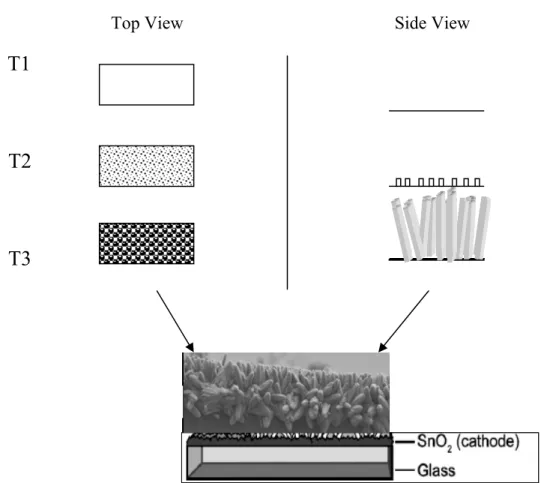
Our group fabricates ZnO thin film by the electrodeposition method using a standard three-electrode cell. (See parts of installation) It comprises a saturated Ag/AgCl three-electrode as a reference electrode, a platinum mesh (grid) used as the counter electrode, and FTO substrate glass as working electrode.
FTO substrates are supplied commercially. Before carrying out experiments, it must be cut into small slices about 1 cm×2cm. The surfaces of samples were not activated and were cleaned following a standard procedure, i.e. the glass substrates were cleaned in common organic solvents in an ultrasonic bath. Acetone, alcohol and Milli-Q water are each used for 5min. After deposition, the samples were rinsed with Milli-Q water so as to eliminate chloride salts present on their surface and dried in a stream of air.
The experimental plan was developed and formulated by means of a literature review (see Appendix Table 4). In order to guarantee the concentration of dissolved oxygen in the electrolyte, pure oxygen gas was charged into the cell over about 35-40 minutes and was the source for the synthesis of oxides before the electro-deposition process was executed. The thin film was grown at a constant potential (-1.0V) and a constant bath temperature (650C) in an aqueous solution of different concentrations of zinc chloride (Supplied 99.999% anhydrous beads of Zinc Chloride by Sigma-Aldrich Inc, USA) and supporting electrolyte (0.1M potassium chloride). Chronoamperometry and potentiostatic
electro-deposition experiments were carried out in a three-necked glass vessel where foams were inserted through the centre neck in order to separate the vessel into three individual compartments. The potentiostat and bath circulators used as this process were the Princeton Applied Research potentiostat /galvanostat( Model 273) and Isotemp 3016, respectively.
3.2 Chemical Characterization
X-ray diffraction
In principle XRD measurements come down to measuring distances between planes with plane x-ray waves (wavelength of a few tenths of a nm). When the Bragg condition nλ =2dsinθ is satisfied and a peak will be measured.
The result of an XRD measurement is a diffractogram, showing phase present (peak positions), phase concentrations (peak heights), amorphous content (background hump) and crystallite size/strain (peak widths).
The morphology of the ZnO is studied with wide-angle x-ray diffraction. A reflection observed in the wide-angle x-ray scan from the different samples. The effects of the chemical bath composition and water content on this reflection were studied
Many properties of Zinc oxide thin film are linked to material contents, structure and morphology. While these properties were measured by XRD, EDS, SEM techniques as well as some instrument such as four- point probe and infrared spectroscopy.
X-Ray diffraction is a versatile, non-destructive analytical technique for identification and quantitative determination of the various crystalline forms, known as ‘phase’, of compounds present in powdered and solid samples.
Identification is achieved by comparing the X-ray diffraction pattern – or ‘dffractogram’ – obtained from an unknown sample with an internationally recognized database containing reference patterns for more than 70,000 phases.
Moden computer-controlled diffractometer systems use automatic routines to measure, record and interpret the unique diffractograms produced by individual constituents in even highly complex mixtures.
XRD used as analysis of chemical composition, relative percentage of phase and orientation. Samples were carried out using XRD with 50 kV and 40mA, Cu Kα radiation, λ=1.5406.. EDS used to identify elements of samples and analyze of small area interested. In practice, it also determines the relative parentage of elements in qualitative analysis. The contents of Zn and O and ratio of them in the thin film were obtained by EDS.
A crystal lattice is a regular three-dimensional distribution (cubic, rhombic, etc.) of atoms in space. These are arranged so that they form a series of paralled planes separated from one another by a distance d, which varies according to the nature of the material. For any crystal, planes exist in a number of different orientations – each with its own specific d-spacing.
Fig. 6 Reflection planes in a cubic lattice
Bragg’s Law (nλ =2dsinθ)
When a monochromatic X-Ray beam with wavelength λ is incident on lattice planes in a crystal at an angle θ, diffraction occurs only when the distance traveled by the rays reflected from successive planes differs by a complete number n of wavelengths.
By varying the angle θ, the Bragg’s law conditions are satisfied by different d-spacings in polycrystalline materials, plotting the angular positions and intensities of the resultant diffraction peaks produces a pattern which is characteristic of the sample, where a mixture of different phases in present, the diffractogram is formed by addition of the individual patterns.
Fig.7 Interference spectrum of Bragg’s law
.
3.3 SEM Characterization
The SEM's principle component is a finely focused electron beam scanned across the surface of the sample generates secondary electrons, backscattered electrons, and characteristic X-rays.. The SEM's primary imaging method is through the collection of those secondary electrons (or backscattered electrons) that are released by the sample. These backscattered electrons are detected by a scintillation material, which is a radiation detector that produces flashes of light from the electrons. The light flashes are then detected and amplified by a photomultiplier tube. These signals are collected by detectors to form images of the sample displayed on a cathode ray tube screen.
Fig.8 Principle of SEM
While SEM used as image of structure, size of grain and distribution. Especially, the thicknesses of thin films were measured by SEM. In order to avoid charging effect caused by secondary electrons-- black rectangles phenomenon. Morphologies were observed by SEM at an acceleration voltage of 10-15 kV, probe current of 6×10⁻¹⁰ Amp. The samples were measured in JSM-840, JEOL SEM equipment.
3.4 Resistivity Measurements
Resistivity measurements were carried out using a Keithley 224 programmable current source and Fluke 8010A digital multi-meter combined with a Signatone S-301-6 four-point probe station. The semiconductor thin film’s resistance was measured using a four-point probe. Optical properties such as transmittance and reflection spectrums were measured by Bruker optics-IFS 66/S infrared spectroscopy. While Nanostructures morphology and semiquantitative analysis were obtained using a JEOL 840A SEM. Diffraction patterns
were observed using a Philips-X’pert x-ray diffractometer. Wavelength of the thin film was measured with a Sciencetech 9055/9055F monochromator.
Computer
Isotemp 3016 Three-necked glass vessel Potentiostat/Galvanostat (Model 273)
Resistivity was performed combined with digital multimeter and programmable current source by establishing conditions at 100 V of voltage and 4×10⁻³ A. Measure method of resistivity followed the normal procedures.[45-47]
3.5 IR Spectroscopy
FTIR spectroscopy is used primarily for qualitative and quantitative analysis of inorganic compounds, and also for determining the optical properties
Because of chemical bonds absorb infrared energy at specific frequencies (or wavelengths), the basic structure of compounds can be determined by the spectral locations of their IR
absorptions. The plot of a compound's IR transmission vs. frequency is its "fingerprint", which when compared to reference spectra identifies the material.
When a molecule is irradiated with infrared radiation, it absorbs at frequencies that correspond to the vibrational / rotational energies of the molecule. Molecular motions that result in infrared absorption bands may be described in terms of bond stretches, bond angle deformations, torsions and rotations. The collection of absorption bands over the IR frequency range (i.e., the infrared spectrum) is characteristic of the structure of the molecule. The infrared spectrum can be used to identify the molecule by comparison to standard spectra or by analysis of specific absorption bands due to functional groups
Transmittance and reflection of ZnO film measurement were carried out using infrared spectroscopy with tungsten source, 32 scans (8500-25000cm-1) and Si diode S510 detector. Blank glass was used as reference.
At the same time, many methods and techniques such as algorithms method, graphic and calculation deduced method, as well as synthetic and analytic method were applied to this study.
CHAPTER 4 RESULTS AND DISCUSSION
The Pourbaix diagrams for aqueous dissolved zinc at concentrations of 5mM, 1mM and 0.5mM at 65oC, are shown in Fig.9 bellow:
Fig9. Effect of the concentration of ZnCl2 (potential / pH diagrams) at 65oC Thin line: 5mM (cross point pH=5.82,
E= -0.835V), middle line: 1mM (pH=6.17, E= -0.858V), thicker line: 0.5mM (pH=6.32, E= -0.868V)
Since a Pourbaix diagram was made by Fact Sage software under same conditions of experiments, deposition temperature was performed at 650C, The formation of Zn (OH)2 is not favored kinetically, it is obvious that there is no existing of Zn(OH)2 in the diagram. From the Pourbaix diagram, Zn2+ is stable at pH from zero to 6.32. Ten-fold change in
ZnCl2 electrolyte concentrations only changes the pH by 0.5 units. With decreasing
concentration of electrolyte, the formation line of ZnO shifts towards higher pH. However, the potential change only marginally, 0.033V. Fabrication of ZnO films by
electro-deposition involves the following electrochemistry:
Zn 2+ + ½ O2 +2e → ZnO (E0 =0.93V/ NHE) Metallic zinc deposition reaction:
Zn 2+ + 2e → Zn (E0 = -0.76V/ NHE)
Therefore, from the standard potential energy perspective, there exists a large theoretical potential window for deposition of ZnO.[48, 49] Electro-depositions are mostly carried out between -1 and -1.3V vs MSE. According to the above Pourbaix diagrams, if one chooses the -1.3V potential, the electrolyte must be much more alkaline (higher pH) to stabilize the ZnO. Thus, it is required that the concentration of ions in electrolyte be higher. Therefore, a potential value -1.0V is the first choice of our experiment.
Overall, pH value will strongly influence electro-deposition redox rates, reaction products and the morphology of the reaction products.
4.1 Chemical Composition of the ZnO Thin Film
The X-ray diffraction pattern and EDX information obtained from the Philips-X’pert and JEOL 840A instruments revealed the characteristics of the ZnO thin film composition. They indicated that this film is made of polycrystalline of the ZnO. X-ray diffraction peaks for ZnO occurring at approximately 340, 360 and 620 2-theta were indexed from pure ZnO( JCPDS data, file number 36-1451, see Appendix 1 Table 3). Fig.10 shows that the most intense diffraction peak is located at 34.330 2 theta indicating that (002) is the preferential crystal orientation with growth along the c-axis perpendicular to the substrate (see
Appendix 1 and Fig.15). In addition, these diffraction patterns completely match the data of Table 1 which derive from theoretical calculations. The sharpness of the peaks in all diffraction patterns of Fig. 10 is evidence of good crystalline material. The first two diffraction peaks at about 34.33 and 36.17o 2-theta are attributed to ZnO. Indexing of the most intense peaks confirm that the formation of crystalline ZnO in the film is similar during the different electro-deposition times of 20min, 40min and 60min. The sample deposited at 60 min is in excellent agreement with the diffraction lines of pure ZnO from both intensity and peak area data.
That is to say, in Fig. 10 Diagram (c), the intensity of the third peak located at about 62.65o 2-theta attributed to ZnO is stronger compared to Diagrams (a) and (b). Especially, the relative intensity of peaks due to ZnO is very similar for Diagrams (b) and (c); these peaks are very narrow with small areas. This indicates that crystals size may be big to compare diagram (a). The higher intensity and the narrower spectral width of the peak are also attributed to better optical properties of the materials. Table 2 also provides data for the relative amounts of all of elements found in the thin films fabricated under the three different deposition conditions. The 5mM group had relatively more ZnO in its chemical composition and the highest peak intensity, and was a close match to the XRD diffraction diagram of pure ZnO. Within the other groups, the 1mM+20min and 0.5mM+40min also produced the highest amounts of ZnO (See Table 2). EDX semi- quantitative analysis showed bright particles and dark particles which respectively represent ZnO nanorods and base background (Also see Table 2). In the 5mM ZnCl2 electrolyte concentration group, the thin film evidently covered the substrate very well since smaller relative amounts of Sn and Si were detected on the top of the films while the other two groups of 1mM and 0.5 mM were obviously worse. This phenomenon might be interpreted by EDS resolution. It is
known that EDS can identify a spot size of a few microns of samples, it detected a small amount of Sn and Si coming from the coated glass substrate (SnO layer) during detector is collecting the characteristic X-ray of Sn and Si elements into an energy spectrum. It is very important is that films of ZnO are of good quality one because these impurities, such as Cl -or other elements cause defects in the thin films (The ohmicity of the contact between substrate and deposited thin film is good when there is no any aid of detects in growth proceeding).
a) 5mM+20min
c) 5mM+60min
Fig.10 XRD diagrams. a) 5mM ZnCl2+0.1M KCl at potential: -1.0V, deposition time: 20 min. b) 5mM ZnCl2+0.1M KCl
at potential: -1.0V, deposition time: 40 min. c) 5mM ZnCl2+0.1M KCl at potential: -1.0V, deposition time: 60 min
Table 1: Characteristics of XRD peaks of thin films prepared by electrodeposition from a 5mM ZnCl2 solution
Deposition
Time (2ºtheta) Position d spacing (Å) Rel.Int (%) (cst/2º theta) Area Chemical Formula Calculations
20 min peak 1 34.3307 2.61327 100 279.98 ZnO (002) peak2 36.1725 2.48433 59.86 263.58 ZnO (002) (101) peak3 37.6954 2.386413 16.93 287.31 No 40 min peak 1 34.3457 2.61109 100 123.26 ZnO (002) peak 2 36.1916 2.48204 40.31 28.98 ZnO (002) (101) peak3 62.651 1.48286 18.48 75.94 ZnO (103) 60 min peak 1 34.32655 2.61358 100 296.88 ZnO (002) peak 2 36.164 2.4849 31.34 103.35 ZnO (002) (101) peak 3 62.6483 1.48292 21.74 38.03 ZnO (103)
Pure glass
5mM+40min
Table2: Semi-quantitative analysis of chemical composition of ZnO thin film by EDX (Condition: WD: 38mm, Accelerate Voltage: 10.0KV, Probe Current: 6×10⁻⁹ A, Aperture: 3, Process Time: 6, Acquisition Time: 60s)
Position General area Bright particles Dark particles
Elements Zn O Sn Si Zn O Sn Si Zn O Sn Si 5mM+20min 66.4 23.9 8.7 0.4 67.2 24.3 7.0 0.7 56.4 24.6 17.4 1.1 5mM+40min 70.6 22.0 5.9 0.7 74.9 21.8 2.7 0.1 73.3 21.1 4.9 0.2 5mM+60min 78.2 20.9 0 0.3 76.5 22.4 0 0.3 78.7 20.1 0 0.3 1mM+20min 19.7 33.6 42.9 3.4 59.0 28.3 11.6 0.9 5.3 36.7 55.0 3.5 1mM+40min 19.0 34.2 44.2 3.7 25.8 32.6 38.9 2.8 2.6 38.2 55.9 3.8 1mM+60min 17.8 34.1 44.0 3.2 33.8 32.0 31.8 2.1 4.0 36.8 55.7 3.6 0.5mM+20min 7.0 37.2 54.7 2.9 12.3 35.5 48.9 3.1 2.1 36.5 56.4 4.4 0.5mM+40min 11.7 33.4 51.0 2.6 28.2 33.5 35.8 2.5 7.4 34.8 53.7 3.8 0.5mM+60min 16.4 34.8 45.0 2.9 15.3 32.3 48.1 3.4 6.3 35.4 54.1 3.5 Pure Glass 38.4 56.4 4.5
4.2 Nanostructure of ZnO Thin Films
According to the Pourbaix diagram, ZnO is formed under the condition of high pH from pH 8 to14. Two equations can explain routes for the contribution of more OH-, i.e. O2 + 2H2O + 4e → 4OH- and SnO2 +2 H2O + 4e → 4OH- + Sn, while SnO2 coming from FTO glass substrate.[46] They created the good formation environment of aqueous solution, That is, higher concentrations of hydroxide ion at the surface drive from oxygen electro reduced at the substrate surface. This kind of reduction reaction may lead to a higher adsorption of hydroxide ion on the substrate and then a higher density formation of ZnO formation. In addition, ZnO deposition possesses 1.64V free energy, a relatively large value that favors thematically ZnO self-regulated growth. The presence of Zn2+ or higher concentration in the deposition solution will accelerate the kinetics’ reaction.[50, 51]
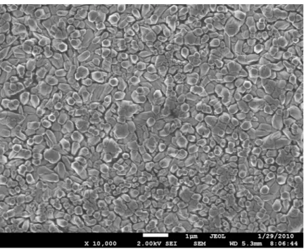
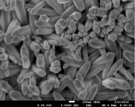
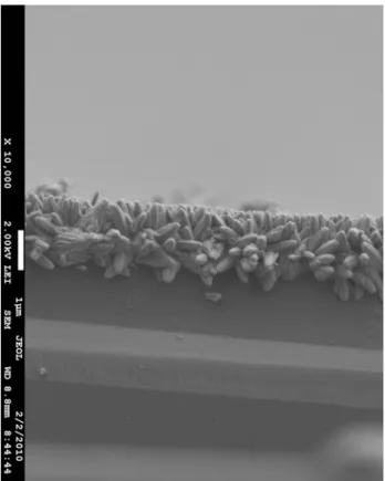
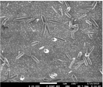
Scanning electron micrographs of ZnO films grown from 5mM bath concentration of zinc chloride are shown in Fig 12. It is observed that many interesting features are revealed in the photos. The prepared semiconductor ZnO film grown on glass substrates of dopped tin oxide contains rod-like morphologies. Discrete nanorods are orientated on the substrate with a little evidence for perpendicular to substrate growth (see Fig. 13 and Fig. 14). The hexagonal and faceted morphology of these grains may be attributed to their wurtzite structures and preferred growth direction (002) during deposition. It is clear that a uniform and compact thin film covered all of the substrate very well in this case (see Fig. 12). The size of nanorods with smooth surfaces increased with the deposition time. For deposition times of 20 min to 40 min, the sizes were 0.673μm and 0.727μm respectively (see Fig. 15).
a) 5 mM+20 min
c) 5 mM+60 min
Fig. 12 SEM top view images of ZnO films from 5mM group electrodeposited at -1.0 Voltage
The thickness of films changed approximately from 0.41μm to 1.636μm. However, the thickness of the film changed very little and exhibited a plateau at 2.11 μm when the deposition time increases from 40 min to 60 min (See Fig. 16 and 17). Meanwhile, one observed that the grain size distribution become more heterogeneous in the bottom image of Fig. 16. However, for the 1mM system, as the deposition time increased, the thickness of the film obviously increased. When deposition times increased from 20min to 40min, both the length and thickness of the nanorods increased slightly. In the system of 1mM+ 60 min, rod length was only about 0.37μm and thickness about 1.0μm. When the concentration of the Zn2+ in the electrolyte was decreased by about 10 orders of magnitude, the morphology
of the ZnO thin films were similar but the amount of rods markedly decreased and a large amount of base grains on the background reappeared. (See Fig. 21)
Many factors can control the film morphology and other important properties. The following sections of the thesis will review the main factors such as deposition time, ion concentration, type of electrolyte and deposition temperature.
Fig. 14 SEM cross-sectional image of ZnO film from 5mM+40min, deposition voltage: -1.0V
b) 1mM+20min (base length 249nm, diameter 96.8nm on base)
c) 1mM+40min
a) 5mM+60min
c) 1mM+20min
Fig. 16 SEM cross-sectional images of measurement of film thickness
a) 0.5mM + 40min (-1.3V)
b) 1mM + 40min (-1.3V)
4.2.1 Influence of the Electrolyte Bath Temperature
We performed the electrodeposition of ZnO at 40, 65 and 90 0C. EDX analysis and patterns showed that there were no any amounts of chloride ion peaks detected in the films deposited at 650C. That confirmed that deposition temperature 650C was reasonable and feasible. In addition, in the range of room temperature, 40 0C and 900C, it was difficult to obtain a homogeneous and well-crystallized zinc oxide film. At 400C or lower temperatures the formation of hydroxide is favored kinetically. While for too high (900C) electrode position temperature, the deposition structures are characterized with coarse crystals formation due to the high growth rate of ZnO. These results are in agreement to what we mentioned previously in the literature review that the deposition temperature plays a key role in the fabrication thin films semiconductors as ZnO thin films.[24] Accordingly both low and high temperatures greatly affect the concentration of dissolved oxygen. First, the deposition temperature is high; the saturated dissolved oxygen markedly decreases. Second, as Goux et al investigated, the curves of the Pourbaix diagram shift towards lower pH. Therefore, Cl- will appear in the deposition bath (ZnCl+ + 2OH- → ZnO +H2O + Cl-) due to ZnCl+ as the major soluble species. During deposition, Cl- might be substitute for oxygen and remain in the thin films. The results explain why the intermediate temperature, i.e. 65 0C is the best temperature for the deposition of thin films ZnO without coarse crystal formation.
4.2.2 Oxygen and Zinc Ion Concentration
Figures 12.b); 13.a) and 16.b) show the SEM pictures of ZnO films electrodeposited at -1.0 V during 40 minutes and 60 minutes at 65 0C. More dense nanorods films are obtained for
the de position with 5mM of zinc ions in the deposition electrolyte. For lower concentrations non homogeneous and non dense films are seen. The results can be explained through the process involved during the electrodeposition.It has been indicated that during the electrodeposition process, there are two different routes as oxygen precursors to obtain zinc oxide.
Oxygen route: Zn2+ + 0.5 O2 + 2 e → ZnO
Nitrate route: Zn2+ + NO3- + 2 e → ZnO +NO2-
Karuppuchamy and Ito[25] reported that a larger surface area of nanorods can be obtained via the oxygen route than the nitrate route with zinc chloride electrolyte. This route may involve some elements which are detrimental to the environment. On the other hand from basic considerations on the formula of ZnO, it appears that during deposition, if one atom of zinc is consumed, it may cause the deposition of an oxygen atom in a 1:1 ratio, which is close to the stoichiometry. Our EDX analysis revealed that for films deposited from 0.5 mM of zinc ions, Zn/O ratio reached about 3 and this experiment showed that there is a deficiency of dissolved oxygen in the electrolyte. In order to guarantee dense rod-like ZnO thin films, we kept the oxygen supply to the electrolyte during the period of deposition and a high concentration of zinc ions, e.g. 5 mM and we found that more dense films were obtained with an increase of oxygen content to a ratio of Zn/O of 1.5. This is in agreement with the idea that dense films are obtained if oxygenshould continue to be supplied to the electrolyte during up to a certain point[48] and employ a high concentration of zinc ion system such as 5mM.
When the zinc ion concentrations are 0.5 mM or lower, the structures of thin films are very compact and smaller. Meantime, the sparse of nanorods were formed. This is an indication that too low Zn2+ concentration may cause no dense distributions of ZnO nanorods in the
dilute system. When the zinc ion concentration is in higher value, it may cause the formation of zinc hydrochloride compounds and inhomogeneous and rough structures due to the increase of the current density and fast deposition rate, as indicated elsewhere.[52] These results are also in agreement with those of Lee at al that shows that the oxygen content in the deposition electrolyte has a great effect on the deposition rate. An increase in the dissolved oxygen leads to a higher growth rate of ZnO at sufficiently high pH.
4.2.3 Influence of the Other Ions in the Electrolyte
As the concentration of the zinc chloride changed from 1mM to 0.5mM, the density of nanorods decreased and the size of nanorods slightly decrease. As speaking from real deposition process, the lower the concentration of primary ions, the lower is the deposition rate (Comparison of 5mM and 1mM’s deposition chronoamperometric current values). The density of product may decrease due to less formation of nucleation in the first stage. As speaking from theoretical concept, interfacial tension controls the thermodynamics and kinetics of nucleation and growth in the deposition system. The chemical composition of the interface changes with changing pH for the precipitation/dispersion process and greatly changes the surface charge density by adsorption of hydroxyl ions. Lower concentration of OH- on the surface in the nucleation stage causing low deposition current might be another reason for the finding of lower density. That is to say, by increasing the ionic strength of the medium, the surface charge may reach its maximum charge density due to electrostatic forces at the interface. As a consequence, the interfacial tension of the system will reach a minimum. Lower interfacial tension leads to an important reduction of the nucleation energy barrier, which in turn leads to a decrease in the average nanoparticle size and increase in number density.
Chloride ion in the medium only affects the morphology making the grain surfaces smooth. With increasing chloride ion concentration, it significantly decreases the molecular oxygen reduction rate because of an adsorption phenomenon of the anion that impedes the reduction rate of oxygen molecular and then decreases the growth of ZnO[26]. The literature indicates that higher or lower KCl concentrations do not affect the growth of ZnO films.[53] While other reports indicate that increased concentration of chloride ion in the bath does not seem to influence the morphology and crystalline orientation of ZnO.[54] This experiment chose 0.1M KCl as the appropriate concentration.
4.2.4 Deposition Time
The thickness of the array film of ZnO nanorods as a function of deposition time was studied in this research. It was found that the film thicknesses increased with increasing deposition time. But the thickness of the thin film changed only marginally when the deposition time changed from 40 min to 60 min. It might be caused by compromise between growth of the film thickness and growth of the rods. The length of nanorods increases with increasing deposition time while the width of nanorods can be changed by modifying the concentration of the precursor. It is not hard to see that the average size of rods increased from 0.673µm to 0.727µm when the deposition time changed from 20 min to 40 min. This corresponds to an average growth rate of about 2.7 nm min-1. It was difficult to identify the broaden tendency of rods from cross-sectional SEM images. Changing from 5mM to 0.5mM, the widths of rods became qualitatively smaller. This trend might be related to the concentration of electrolyte and process of second nuclei formation.