Université du Québec
Institut National de la Recherche Scientifique Center for Energy Materials and Telecommunications
Dynamics of semiconducting nanocrystals uptake into
mesoporous TiO
2thick films through electrophoretic deposition
and its application in solar energy
By Lei Jin
A thesis submitted to the Department of Energy, Materials and Communications in conformity with the requirements for the degree of Master of Philosophy
Advisory Committee:
President of the jury Mme Ana Tavares
internal examiner INRS-EMT, Université du Québec
External examiner M. Richard Ares
Université de Sherbrooke
Internal examiner Mme Ana Tavares
INRS-EMT, Université du Québec Director of Research M. Federico Rosei
INRS-EMT, Université du Québec Codirecteur de recherche Mme Dongling Ma
INRS-EMT, Université du Québec M. Alberto Vomiero
Luleå University of Technology
ACKNOWLEDGEMENTS
It is my great honor to spend one year and half to accomplish my graduate studies at Centre for Energy, Materials and Telecommunications, Institut National de la Recherche Scientifique (INRS-EMT), University of Quebec, Canada. Foremost, I would like to express my sincere gratitude to my supervisor, Prof. Federico Rosei, for continual guidance and support throughout the duration of my Master and research. Professionally, Dr. Rosei has supported me not only by providing systematic guidance and great effort in the scientific field, but also by offering me a chance to be a group coordinator to develop my social skills. And personally, he has always been a strong supporter and friend when I needed help. It is one of the most valuable experiences in my life being able to study under his supervision.
Besides my advisor, my sincere thanks also go to Prof. Alberto Vomiero, for his patience, motivation, enthusiasm, and immense knowledge. His guidance helped me in all the time of research and writing. I could not have imagined having a better development for my Master study without him.
I would also wish to give special thanks to the contributions to this work made by Dr. Haiguang Zhao, who made vital contributions and offered invaluable help and comments on my research.
I would like to acknowledge Prof. Dongling Ma, my co-supervisor at INRS-EMT, for her kind help and important comments on my project research. I am also grateful to all the group members from NFL (NanoFemtoLab) for their help throughout the work as well as other collaborators. Massive thanks to the departmental and technical staffs at INRS-EMT and all my friends who have made my research life so enjoyable.
Last but not least, I would like to give special thanks to my family: my parents Xiaoli Xing and Junli Jin, my sister Dong Jin, for their continuing love and heartily support. I also wish to express thanks to my Fiancé, Yang Liu, who loves me deeply and supports me selflessly. I thank my family and friends for supporting me spiritually throughout my life.
ABSTRACT
Quantum dots (QDs), have been recognized as one type of the most promising photosensitizer for photoanode fabrication due to their unique and scalable optical properties where photoluminescence and absorption of the QDs are size-tunable. However, there are several major concerns with QD sensitized photoanodes: First, QDs should be deposited into mesoporous films effectively and without aggregation; Second, QDs have to be bound strongly onto mesoporous films; Last but not least, the charge transfer kinetics between QDs and wide-band-gap semiconductor has to be fast in order to achieve a highly efficient photoelectrode. The search for methods to achieve these requirements is attractive and challenging. Electrophoretic deposition (EPD), which is a straightforward technique for the uptake of nanoparticles into mesoporous films, has demonstrated highly effective in the preparation of high-efficiency QD-sensitized photoanodes. EPD consists in the application of an external potential between two electrodes immersed into a solution of the particles to be uploaded. Charged particles (both positive and negative) undergo a driving force that induces their penetration and grafting into the mesoporous photoanode. Unlike prior chemical linker-based methods, EPD does not require pretreatment of the TiO2, and deposition time as short as 1 h is
sufficient for effective coating. After EPD, the photoanode typically exhibits a high optical density, leading to complete absorption of solar radiation in the absorption range of the QDs. Despite the remarkable results obtained in terms of photoconversion efficiency (PCE), no systematic investigation is reported in literature on EPD of nanoparticles in mesoporous films so far. In the present thesis, we addressed this open issue and gave an exhaustive description of the phenomenon from the experimental point of view as well as from the point of view of the modeling of the physical chemical processes occurring during EPD. We investigated the uptake of colloidal QDs into TiO2 films using
EPD. We examined PbS@CdS core@shell QDs, which are optically active in the NIR region of the solar spectrum and exhibit much increased long-term stability toward oxidation compared to their pure PbS counterpart, as demonstrated by X-ray photoelectron spectroscopy (XPS) and photoluminescence (PL). We applied Rutherford backscattering spectrometry (RBS) to obtain Pb depth profile into the TiO2 matrix. The
applied electric field induces the fast anchoring of QDs to oxide surface. Consequently, QD concentration in the solution contained in the mesoporous film drastically decreases, inducing a Fick-like diffusion of QDs. We modelled the entire process as a QD diffusion related to the formation of QD concentration gradient, and a depth-independent QD anchoring. EPD duration and applied voltages in the range 5 to 120 mins and 50 to 200 V were considered. Furthermore, we were able to determine the electric field-induced diffusion coefficient D for QDs and the characteristic time for QD grafting, in very good agreement with experiment. D increases from (1.5±0.4)×10-5 µm2 s-1 at 50 V to (1.1±0.3) ×10-3 µm2 s-1 at 200 V. These results quantitatively describe the process of QD uptake during EPD, and can be used to tune the optical and optoelectronic properties of composite systems, which determine, for instance, the PCE of the photoanodes. The dynamics of EPD could also be applied to other different colloidal nanoparticles and quantum rod materials for sensitization of mesoporous films. In addition, we also demonstrated the increased stability of the core@shell structure compared to PbS QDs after EPD in terms of structure and optical properties. Based on our previous studies that confirmed a fast charge transfer from PbS@CdS to TiO2, PbS@CdS sensitized
photoanodes can be strong candidates for the development of highly efficient and stable photoanodes in PV devices and photoelectrochemical (PEC) H2 generation.
KEYWORDS: electrophoretic deposition, quantum dots, solar cells, quantum dot sensitized solar cell.
TABLE OF CONTENTS
ACKNOWLEDGEMENTS ... II ABSTRACT ... III TABLE OF CONTENTS ... V LIST OF TABLES ... VII LIST OF FIGURES ... VII LIST OF EQUATIONS ... X LIST OF ABREVATIONS ... XI
1. INTRODUCTION ... 1
1.1 QUANTUM DOTS (QDS)SENSITIZED PHOTOELECTRODES ... 1
1.1.1 QDs work as light harvesters in solar cells (SCs) ... 1
1.1.2 QDs work as photosensitisers for H2 production ... 8
1.2 CHALLENGES IN QDS SENSITIZED PHOTOANODES ... 10
1.2.1 Light harvesting ... 10
1.2.2 Uptake QD into mesoporous films ... 11
1.2.3 Stability ... 12
1.3 THESIS OBJECTIVES AND CONTRIBUTIONS ... 13
1.4 THESIS ORGANIZATION ... 13
2. EXPERIMENTAL ... 15
2.1 MATERIALS ... 15
2.2 QDS AND TIO2 FILMS PREPARATION ... 15
2.2.1 Synthesis of PbS QDs ... 15
2.2.2 Synthesis of PbS@CdS QDs ... 16
2.2.3 Mesoporous TiO2 films preparation ... 17
2.2.4 Uptake QDs into the mesoporous TiO2 films thorugh EPD ... 17
2.3 CHARACTERIZATIONS ... 18
2.3.2 Transmission Electron Microscopy (TEM) ... 19
2.3.3 X-ray Photoelectron Spectroscopy (XPS) ... 19
2.3.4 Rutherford backscattering spectroscopy (RBS) ... 20
2.3.5 UV-visible (UV-vis) Spectroscopy ... 22
2.3.6 Photoluminescence (PL) Spectroscopy ... 22
3. DYNAMICS OF QD UPTAKE INTO MESOPOROUS TIO2 THICK FILMS THROUGH EPD ... 23
3.1 SYNTHESIS AND CHARACTERIZATION OF QDS IN SOLUTION AND IN TIO2 FILMS ... 23
3.2 QDSTABILITY AFTER EPD ... 26
3.3 DYNAMICS OF EPD ... 28
4. PROMISING APPLICATIONS ... 37
4.1 QDSCS FABRICATION ... 37
4.2 WATER SPLITTING ... 39
5. CONCLUSION AND FUTURE PERSPECTIVES ... 41
5.1 CONCLUSION ... 41
5.2 PERSPECTIVES ... 42
6. REFERENCES ... 44
LIST OF TABLES
Table 3.1 Dimensions and optical properties of pure and core@shell QDs investigated in this study. The overall size of PbS@CdS QDs is determined based on TEM observation, the core size is estimated from the position of the first excitonic peak and the shell thickness is estimated by simple subtraction. To identify the different samples, S M L labels are used according to their small, medium and large size, respectively. ··· 24 Table 3.2 PbS concentration and diffusion coefficient D as a function of the applied voltage in EPD. ··· 33
LIST OF FIGURES
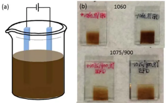
Figure 1.1 Image showing (a) colloidal PbS quantum dots. Inset: TEM image with resolution of 1.5 nm; (b) splitting of energy levels in QDs due to the quantum confinement effect, semiconductor band gap increases with decrease in size of the nanocrystals [22]; (c) solar spectrum [23] and corresponding tunable absorption spectra of QDs. ··· 3 Figure 1.2 Scheme (not to scale) of (a) QDSCs. Black arrows around the cell perimeter denote direction of electron flow (b) the energetics which drive electron and hole transport in a QDSCs. [25] ··· 4 Figure 1.3 The equivalent circuit of a solar cell.[32] ··· 7 Figure 1.4 Getting the important parameters From the I-V Sweep. [34] ··· 8 Figure 1.5 Band-edge positions of semiconductor photocatalysts relative to the energy levels of various redox couples in water. [40] ··· 9 Figure 2.1 Image showing the air-free reaction setup for synthesizing PbS QDs. [90] ·· ··· 16 Figure 2.2 Cation exchange approaches for transferring PbS QDs into PbS@CdS. · 16 Figure 2.3 (a) Illustration of the EPD system; (b) images of QDs/TiO2 electrodes after
1 h of EPD, red and black labels corresponding to samples produced from positive and negative electrode of applied bias. ··· 18 Figure 3.1 Size distributions of (a) PbS_M and (b) PbS@CdS_M QDs. ··· 23
Figure 3.2 Absorption spectra of (a) PbS and PbS@CdS QDs in solution. (b) Representative TEM image of PbS@CdS QDs. (c) EDX analysis of PbS@CdS QDs with ~3.0 nm core diameter (shell thickness ~0.2 nm) after anchoring to TiO2
nanoparticles by using EPD for 30 min (negative TiO2 electrode). Inset: SEM
cross-section of a TiO2 film. ··· 24
Figure 3.3 Representative TEM images of PbS@CdS QDs loaded into TiO2 at four
different EPD durations (negative TiO2 electrode): (a) 10 min (b) 30 min (c) 60 min (d)
120 min. Inset of (d): enlarged TEM image. The red circles highlight the presence of the QDs. (e) Dark field Scanning TEM image of TiO2 nanoparticles covered by QDs.
The high contrast between the TiO2 and QDs allow precise identification of the
position of the QDs on the surface of TiO2 nanoparticles. ··· 25
Figure 3.4 High resolution Pb 4f core level spectra Photoelectron spectra after correction of electrostatic charging obtained from (a) PbS_M quantum dot (b) PbS@CdS_M core@shell quantum dot on silicon (up) and upload into TiO2 with EPD
(down). ··· 27 Figure 3.5 PL of (a) PbS_M QDs and (b) PbS@CdS_M QDs just after EPD and after 24 hours exposure to air. Benchmarking PL spectra of QDs in solution is also reported. ··· 28 Figure 3.6 (a) RBS spectrum of TiO2 mesoporous film sensitized with QDs for 120
minutes. The red curve is the RUMP code simulation. The surface edges for Ti, Cd and Pb are indicated by arrows. (b) RBS signal of the spectral region pertaining Pb signal for samples sensitized at different durations (5, 10, 30, 60, 120 minutes, from dark blue to light azure). A and B rectangles highlight the two different regions in which QD diffusion cannot be detected (A) or is clearly visible (B). ··· 29 Figure 3.7 Pb atomic ration as a function of EPD time at the interface of TiO2/FTO for
PbS@ CdS_L (red line) Black line corresponding to the change of the curvature. ···· 30 Figure 3.8 Pb atomic ration as a function of EPD time at the surface of TiO2 film of
PbS@CdS_L ··· 30 Figure 3.9 (a) Position of the parameter x0 as a function of EPD time. Inset: illustration
of the procedure to determine x0 from a standard RBS spectrum. (b) Parameter x0
depth and simulated yield (red solid line) obtained from the diffusion coefficient D and the characteristic decay time τ obtained from RBS data. The two different components contributing to the curve are reported: diffusion process of Pb from solution (red dotted line) and position-independent QD uptake (red dashed line). (d) Experimental (solid lines) and simulated (dashed lines) Pb yields for the complete series of EPD samples.
··· 31 Figure 3.10 Pb distribution versus time and depth in TiO2 film under three different
perspectives, based on the experimental parameters calculated for 200 V applied bias. ··· 34 Figure 3.11 (a) x0 versus square root of EPD time. (b) Diffusion coefficient D versus
EPD voltage, and (c) Pb concentration versus depth at three different EPD voltages after 60 min EPD. Symbols: experiment; solid lines: simulations according to the values of D reported in Table 3.2 (d) Fraction of Pb introduced in the film by diffusion (PbDiff,) at different voltages. PbDiff and the total Pb amount are calculated as the
integral of Pb concentrations along film depth based on the two components illustrated in Figure 3.9 (c). ··· 35 Figure 4.1 Scheme of the QDSCs. ··· 38 Figure 4.2 J-V characteristics of QDSCs fabricated with PbS@CdS QDs-decorated TiO2 (device was coated with CdS and ZnS) under AM1.5G illumination with light
intensity of 100 mW/cm2. ··· 39 Figure 4.3 (a) Photocurrent density versus the applied voltage referenced to RHE and (b) photocurrent responses at 0.2 V vs RHE of TiO2/colloidal QDs photoanode. ··· 41
LIST OF EQUATIONS
Equation 1.1 ... 2 Equation 1.2 ... 5 Equation 1.3 ... 5 Equation 1.4 ... 5 Equation 1.5 ... 5 Equation 1.6 ... 5 Equation 1.7 ... 6 Equation 1.8 ... 6 Equation 1.9 ... 6 Equation 1.10 ... 6 Equation 1.11 ... 8 Equation 1.12 ... 8 Equation 3.1 ... 31 Equation 3.2 ... 32 Equation 3.3 ... 33LIST OF ABREVATIONS
ATW...Atmospheric Thin Window CB...Conduction band CBD...Chemical Bath Deposition CE...Counter electrode DA...Direct Adsorption DI...Deionized DSSCs...dye-sensitized solar cells EDX...Energy-dispersive X-ray spectroscopy EIS...Electrochemical Impedance Spectroscopy EL...Electrolyte EPD...Electrophoretic deposition FF...fill factor FTO...Fluorine doped tin oxide HRSEM...High Resolution Scanning Electron Microscope Imax...maximum current
ISC...short circuit current
MAA...Mercaptoacetic acid NIR...Near Infrared OA...Oleic Acid ODE...Octadecene OLA...Oleylamine PCE...Photoconversion Efficiency PEC...Photoelectrochemical
PL...Photoluminescence PV...Photovoltaic QDs...Quantum dots QDSCs...Quantum dot-sensitized solar cells QY...quantum yield RBS...Rutherford backscattering spectrometry redox...reduction-oxidation SEM...Scanning Electron Microscopy SILAR...Successive Ionic Layer Adsorption and Reaction SCs...Solar Cells TEM...Transmission Electron Microscopy (TMS)2S...Bis (trimethylsilyl) sulfide
TOP...trioctylphosphine UV-vis...UV-visible VB...valence bands Vmax...maximum voltage
Voc...open circuit voltage
wbSC...wide-bandgap semiconductor XPS...X-ray Photoelectron Spectroscopy
1.
INTRODUCTION
1.1 Quantum Dots (QDs) Sensitized Photoelectrodes
Limiting the global temperature increase is one of the biggest challenges in the 21st century. [1] To limit increases in greenhouse gas (CO2) emissions, alternative energy
sources to coal, oil and gas must be provided, such as power from wind and water, biomass, or solar energy. Compared to other clean sources, solar energy can provide our planet with about 10,000 times more energy than our global daily consumption. [2]
In view of the intermittent nature of solar energy and our power consumption, the idea to convert light into electric power or chemical fuels is attracted raising awareness.
1.1.1 QDs work as light harvesters in solar cells (SCs)
It was not until 1839 that the photovoltaic (PV) effect was first discovered by French Physicist A. E. Becquerel, [3] essentially marking the dawn of human-based utilization of solar radiation. [4] A fundamental understanding of this phenomenon, given by Albert Einstein [5], paved the route for Bell Labs to develop a silicon PV cell [6] — the first solar cell capable of generating enough power from the sun to run electrical equipments every day. Solar panels based on this silicon p-n junction technology has attracted a lot of attention over the last few years and their commercially available efficiency has reached to 22%. [7] However, this class of PV devices suffers from problems of inherent limitations in silicon as a material, competing demand for high-grade silicon wafers, and high manufacturing costs. Herein further advancement in the research and development of new PV cells is required to increase the light to electric power conversion efficiencies and to reduce the price of solar panels.
The second generation PV devices consisting of polycrystalline semiconductor thin films, including amorphous silicon, Cu/In/Ga/Se (CIGS cells) and CdTe, which can bring down the price significantly, but their typical performance is 10 - 15% which needs to be enhanced for making them practically viable. [8, 9] In addition, the production of the second generation PV cells still requires vacuum processes and high temperature
treatments, resulting in a large consumption of energy associated with the scarce elements. Over the last few years, an intense worldwide effort was geared towards developing third generation PV cells by using wet chemistry synthetic routes for the preparation of suitably tailored nanomaterials.[10-19] Among the candidate sensitizers, QDs have attracted widespread attention, benefiting from its special optical properties.
[20] Typically, a bulk semiconductor has continuous conduction and valence energy bands, separated by a fixed energy gap, Eg, which is the minimum energy required to excite an electron. The absorption of a photon with energy greater than the band gap energy could contribute to the excitation of an electron, leaving an orbital hole in the valence band to form an electron-hole pair (exciton), which has a finite size defined by the exciton Bohr radius (as shown in Figure 1.1 (b)). In bulk materials, the crystal lattice is much larger than the exciton Bohr radius, allowing free and independent movement of the exciton. However, in a QD, the size of the lattice is at or below the materials’ exciton Bohr radius, translating the exciton to a confined volume less than what it naturally wants to occupy. This “confinement effect” results in particle-in-a-box like behavior, exhibiting as discrete energy levels (as opposed to a continuum of energy levels in a bulk sample, Figure 1.1 (b)). Specifically, the smaller the diameter of the QD is — the stronger the confinement is — the larger the bandgap of the QD is (Figure 1.1 (b)), as described in Equation 1.1 [21]:
E = Eg + (ħ22 / 2R2) (1 /me+ 1 /mh) -1.8e2 /R Equation 1.1
where Eg is the band gap energy of the corresponding bulk material, ħ is the Plank
constant, me and mh are the effective mass of electron and hole, respectively, e is the
charge of the electron, and R and are the radius and dielectric constant of QDs respectively. In other words, QDs with dimensions smaller than the exciton Bohr radius show size-dependent absorption. Therefore, if each single QD materialcan convert one region of the solar spectrum efficiently with the use of a single bandgap, then in theory, a high efficiency of light collection can be achieved by changing the bandgap of the material (Figure 1.1 (c)), which means by changing only the composition and nanoparticles’ size of QDs. Benefiting from the ability to tune the optical properties of
QDs by manipulating their sizes and compositions, QDs were introduced into third generation solar cells as sensitizers.
Figure 1.1 Image showing (a) colloidal PbS quantum dots. Inset: TEM image with resolution of
1.5 nm; (b) splitting of energy levels in QDs due to the quantum confinement effect, semiconductor band gap increases with decrease in size of the nanocrystals [22]; (c) solar spectrum [23] and corresponding tunable absorption spectra of QDs.
1.1.1.1 Construction of quantum dot-sensitized solar cells (QDSCs)
As a cost-effective alternative to silicon-based PV cells, QDSCs can be regarded as a derivative of dye-sensitized solar cells (DSSCs) which was first reported by O’Regan and Grätzel in 1991. [24] Nanostructured wide-bandgap semiconductor (wbSC), such as TiO2 (3.2 eV),which forms into a highly porous nanocrystalline, had been selected as
the sensitizer scaffold, due to their high surface to volume ratio (their real surface area is larger than their geometric area). Figure 1.2 (a) shows a scheme of the basic design of a QDSC. The QD-sensitized nanostructures are immersed into the reduction-oxidation (redox) electrolyte, and the circuit is closed by a counter electrode (CE). The QDs, which graft to the surface of wbSCs, absorb light and create an exciton. Then the exciton dissociation occurs at the QD/wbSC interface, and the resulting electron is
injected from excited levels of QD into the conduction band (CB) of the wbSC. A liquid electrolyte completes the electrochemical system and allows QD neutralization after electron injection.
Figure 1.2 Scheme (not to scale) of (a) QDSCs. Black arrows around the cell perimeter denote
direction of electron flow (b) the energetics which drive electron and hole transport in a QDSCs. [25]
1.1.1.2 Electron Transfer Reactions within QDSCs
To understand the effect of energetics on solar cell, an energy diagram was shown in Figure 1.2 (b)), with a direct view on the energetics of the working electrode, QDs sensitizer, the TiO2 scaffold film, the electrolyte as well as the counter electrode. When
the CB and valence bands (VB) of QDs and TiO2 match suitably, the electrons and
holes can accumulate in two separate particles, allowing high possiblities to be captured at the surface of working electrode. In order for the reactions to take place, the CB of QDs must lie above the CB of TiO2, and redox potential of the electrolyte must lie
between valence band of QDs and conduction band of TiO2. Then once the QDs are
excited, electrons and holes can be energetically drawn to transfer to lower energy states (more negative in vacuum scale) and higher energy states (more positive in vacuum scale) respectively.
If we consider the reactions in an ideal manner: the electron travels from the QDs, through the external circuit, the electrolyte, and back to the QDs; in parallel, the hole travels in the opposite direction, then the reactions contributing to the ideal device performance can be figured out as below:
a) QD is excited by absorbing a photon with energy higher than its bandgap, converting solar energy present in an electromagnetic wave to the potential energy difference between an electron and a hole:
* QD hv
QD Equation 1.2
b) An electron-hole pair in the form of an exciton, or an electrostatically bound pair is formed after the absorption event immediately. If the characteristic exciton binding energy of materials is less than the available thermal energy present in the system, the exciton can dissociate into free carriers: [26, 27]
* *
* QDe h
QD Equation 1.3
c) The electron can be transferred from a thermally excited state within the QD to the CB of TiO2, a process known as hot electron injection: [28, 29]
* 2 * 2 * * h TiO QDh TiO e e QD Equation 1.4In the absence of this reaction above, thermally excited electrons (holes), can transfer a portion of their potential energy to heat and then energetically move from the quasi-continuum of states, which are above (below) the CB (VB) band edge, to their lowest energy configuration at the CB (VB) band edge: [30, 31]
e h
QD
e h
heatQD * *
Equation 1.5
The photogenerated electron can be transferred from the QD to TiO2, resulting in
spatial charge separation:
eh
TiO QD
h TiO
ed) The mesoporous morphology of TiO2 provides a high surface area for QDs uptake,
so that the photogenerated electrons injected into its neighboring TiO2 should
transport through other TiO2 particles before being collected at the working
electrode:
e
TiO
e
nearestTiO
2
2 Equation 1.7
e) During the migration to the working electrode, the electrons can also have possibility to be transferred to the electrolyte molecules which are in contact with the TiO2,
reducing the electrolyte:
→ Equation 1.8
f) The reduced electrolyte should spatially diffuse through the liquid portion of the device:
Equation 1.9
g) When a QD with a photogenerated hole comes across with the reduced electrolyte, the electrical circuit is closed, accompied by the regeneration of the QDs:
ℎ → Equation 1.10
1.1.1.3 The I-V characteristics of QDSSCs
PV cells are devices that absorb photons from a light source and release electrons, causing an electric current to flow once the cell is connected to a load. To understand the electronic behavior of a solar cell, a electrically equivalent model based on discrete electrical components can be established, as shown in Figure 1.3. It is evident that the current produced by the solar cell is equal to that produced by the current source, minus that which flows through the diode, minus that which flows through the shunt resistor.
Figure 1.3 The equivalent circuit of a solar cell. [32]
To characterize solar cells, the most obvious and important measures is the total amount of electrical power produced for a given amount of solar power shining on the cell, which is known as the photoconversion efficiency (PCE). Electrical power is the product of current and voltage, so the maximum values for these measurements are important. In theory, the maximum voltage (Voc) generated by QDSCs is simply the
difference between the (quasi-) Fermi level of the QD seisitized TiO2 and the redox
potential of the electrolyte. Although the QDs can convert absorbed photons into free electrons in the TiO2, only photons with energy higher than the bandgap of QD
ultimately produce current. The rate of photon absorption depends upon the absorption spectrum of the sensitized TiO2 layer and upon the solar flux spectrum. The overlap
between these two spectra determines the maximum possible photocurrent (Isc). To
determine the maximum power from a QDSCs, a parameter which in conjunction with Voc and Isc, was defined as "fill factor" (FF). These important parameters about the cell’s
performance, including its maximum current (Imax) and voltage (Vmax), open circuit
voltage (Voc), short circuit current (ISC), FF and its PCE (by dividing a cell's power output
(in watts) at its maximum power point (Pm) by the input light (E, in W/m2) and the surface
area of the solar cell (Ac in m2)), are derived from the current-voltage (I-V)
characterization of a solar cell, which is the superposition of the IV curve of the solar cell diode in the dark with the light-generated current, [33] as shown in Figure 1.4.
Figure 1.4 Getting the important parameters From the I-V Sweep.[34]
Regarding the solar cell as an ideal diode under illumination, the relationship between dark saturation current and Voc can be inferred from the equation:
J 1 Equation 1.11
where is the dark saturation current density (A/cm2), is the short circuit current density (A/cm2), and is the ideality factor. Assuming that the is voltage independent and ≫ , the is then given by setting J to 0:
Equation 1.12
From equation Eauation 1.12, is proportion to , and therefore needs to be as small as possible to maximize .
1.1.2 QDs work as photosensitisers for H2 production
In view of the intermittent nature, convenient transportation and night-time use of solar energy, the search for method to convert solar energy into a storable form is attractive and challenging. [35, 36] Photoelectrochemical (PEC) solar driven hydrogen production with semiconductor materials [37] appears to be a much more attractive route because the use of H2 chemical bonds to store solar energy combines the
having clean water as the only by-product. [38, 39] Generally, PEC cell presents redox reactions driven by electron-hole pair created by incident photons, namely, the holes oxidize water/hole scavenger at the surface of the photoanode, and the electrons migrate to the counter electrode to reduce water and produce hydrogen. Herein, what is needed and challenging is the development of inexpensive semiconducting materials with suitable conduction and valance band energies, which have not only strong sunlight absorption and effective charge separation, but also high photochemical stability.
Figure 1.5 Band-edge positions of semiconductor photocatalysts relative to the energy levels
of various redox couples in water. [40]
Since the Honda-Fujishima effect of water splitting using a TiO2 electrode was
reported in the early 1970s [38], extensive efforts have been made to construct an efficient PEC water-splitting system and to develop new semiconductor materials for efficient photoelectrodes. The aim of PEC material fabrication is to design a photoelectrode that has the potential to satisfy most of the requirements [ 41]: (a) sufficient visible light absorption (i.e. band gap) in the range of 1.5 to 2.0 eV; (b) efficient separation of photo-generated electron-hole pairs and fast transport of electrons and holes to prevent their recombination; (c) favourable alignment of conduction and valence band edge position with respect to redox potential of water and the resultant photovoltage output to drive the reaction; (d) non-corrosive and high chemical stability in
the electrolyte; and (e) low cost. Figure 1.5 lists bandgap, energy levels of the current photoelectrode materials that researchers focused on. Upon examining several typical semiconductors for PEC applications, the choice of available materials with band gaps ranging between 1.5 and 2.0 eV is limited and thus new semiconductors with narrow bandgap and novel configurations for photoelectrode are needed for practical applications.
Numerous studies have reported large band gap semiconducting oxides such as TiO2
can be developed for H2 evolution with long-time stablility in aqueous electrolyte [42]
However, PEC utility of TiO2 is limited by its UV-responsive band gap of approximately
3.2 eV. Therefore much effort has been made in the attempt to prepare TiO2-based
photocatalysts that can efficiently improve light absorption in a broader spectral region. Such efforts include doping TiO2 with metal/nonmental ions to induce a red shift to the
band gap, [43, 44, 45] and coupling TiO2 with lower-band-gap semiconductors. [63, 46]
Among the low-band-gap semiconductors, the QD is an attractive semiconductor as their band gap is dependent on their size (Figure 1.1 (b,c)) and the existing technology can produce QDs optically active in the visible and near infrared (NIR) spectral region.
1.2 Challenges in QDs sensitized photoanodes
1.2.1 Light harvestingAn intense effort to boost the development of PV architectures [10-13] and PEC photoanode [47-50] lies on application of chalcogenide QDs, including CdS, CdSe and CdTe as light harvesters to sensitize TiO2, forming a convenient heterostructured
platform. However, these QDs are optically active in the visible range. Effectively, photons with energies lower than the bandgap do not get absorbed, in other words, QDs are optically active in the visible region largely ignores NIR light and wastes about 40 percent of the solar energy reaching Earth's surface, reducing output. Herein, QDs that are optically active in the NIR spectral region, such as PbS [51] and PbSe [52] have attracted enormous interest as sensitizers in recent years, while the investigations are still limited so far.
1.2.2 Uptake QD into mesoporous films
In a particular configuration of QD sensitized photoanode, [53] the QDs are grafted on the surface of a wide band gap semiconductor, [54, 55] absorbing light and creating an exciton. Then exciton dissociation occurs at the QD/oxide interface, and then the electron is injected into the oxide that acts as electron transporter. [56] For this reason, one of the important challenges is to apply a low-cost process to incorporate QDs onto the oxide and to achieve effective QD-electrode junctions that would promote charge separation, while minimizing surface charge trapping and charge losses.
In situ growth methods have been widely used to prepare QD-decorated TiO2
photoanodes, including chemical bath deposition (CBD), [57, 58] and successive ionic layer adsorption and reaction (SILAR). [59, 60] Although a direct contact between the oxide and the QDs is achieved in this way, there is no independent control of QD coverage and size. [13] These drawbacks can be avoided if QDs are synthesized in form of colloids before sensitization of the oxide, and then grafted onto the oxide surface. Typically, three main different techniques are used for preparation of colloidal QD-decorated oxide thickfilms: linker-assisted adsorption, [58, 61] direct adsorption (DA), [62] and electrophoretic deposition (EPD). [63] In most cases, the attachment of the QDs to the mesoporous electrode is achieved by using a molecular linker between QD and the oxide particle, and one to several days are needed to achieve the desired coverage and photoanode optical density for QDs with hydrophobic ligand. [64] In case of hydrophilic ligands, QD uptake is typically much faster (several hours), [ 65 ] but the linker molecule may act as a barrier for electron injection, affecting the photovoltaic properties. [66] DA method is based on solvent/non-solvent precipitation of QDs from the solution into the mesoporous film: the tendency of the QDs to agglomerate in solution may lead to uneven and polydisperse surface coverage. [67] EPD, a widely used technique, is based on the motion and grafting of charged particles under an applied electric field, and presents several advantages over the other methodologies, such as the low cost, short duration of the process,
simple equipment, homogeneous surface coverage and formation of a uniform QD layer of controlled thickness. [68, 69]
EPD was previously employed to deposit semiconducting, [70, 71]metallic, [72, 73]
and insulating [74, 75]nanoparticles on conductive substrates or polymers film. [73, 76] The first application of EPD for solar cells was reported for the deposition of TiO2
nanoparticles. [74] Colloidal CdSe QDs were deposited via EPD on a flat thin film as a proof of concept for PV applications, yielding low PCEs (~10−6 %) due to the very low optical density of the solar cell. [77] In order to increase the active area, CdSe QDs were incorporated into porous TiO2 layers several microns thick, [63]reaching
efficiencies as high as 1.7%, under 1 sun illumination. Mora-Seró and co-workers [78]
have prepared QDs sensitized photoanodes by depositing the colloidal PbS and PbSeS QDs into TiO2 mesoporous film via EPD. A strong relationship between QD
sizes, EPD time and device performance was observed, clearly identifying the factors in EPD that are essential for the successful development of QDs sensitized photoanodes. In addition, the decrease of recombination resistance with EPD time unambiguously demonstrated that conformal coverage of TiO2 surface would reduce
charge recombination from TiO2 to electrolyte. [79] For these reasons, suitable control
of the parameters determining QD uptake and oxide coverage is mandatory. However, so far, only generic demonstration of almost constant QD penetration into films is claimed, based on low-resolution X-ray spectroscopy (EDX) analysis, [77] and no systematic investigation of QD uptake is found in literature.
1.2.3 Stability
One of the biggest challenges for bith PV devices and PEC H2 production is the
development of a long-term stable photoanode. In fact, QDs, owing to their large surface-to-volume ratio, are very sensitive to surface defects and oxidation, which cause charge trapping, [80] leading to decrease of PCE. [81] For this reason, QDs are typically capped with organic surface ligands, [ 82 , 83 ] while the dangling bonds remaining on the QD surface can act as carrier trapping sites if partial ligand un-passivation occurs. [84] Recent studies [85, 86, 87] have revealed that a robust, larger band gap inorganic shell can provide more complete passivation for the QD surface,
contributing to largely improved chemical, thermal, photochemical stability, and acceptable charge injection rate in QDs with suitable core size and shell thickness. [88]
1.3 Thesis objectives and contributions
To address all these challenges and issues, I investigated more deeply on QDs sensitized photoanodes by coupling high-quality PbS or PbS@CdS quantum dots into TiO2 thick mesoporous films. The objectives of the projects are the following:
1) Synthesize high-quality PbS and PbS@CdS core@ shell QDs, characterize their structure and properties.
2) Uptake of ex-situ PbS or PbS@CdS QDs into TiO2 mesoporous thick films using
EPD and investigation the distribution and stability of QD after EPD.
3) A systematic investigation of the dynamics of NIR QDs loaded into TiO2
mesoporous film via EPD.
4) Investigation of the influence of EPD time and voltage on the QD uptake process by using PbS@CdS core@shell QDs as highly stable light harvesters.
5) Applied the EPD dynamic to prepare QD sensitized photoanodes with suitable control over QD uptake and oxide coverage, for PV devices fabrication and PEC H2
production.
1.4 Thesis Organization
This thesis is divided into five parts and organized as follows:
Chapter 1 introduces the topic of this thesis and outlines the motivation for this work. Chapter 2 describes the experimental details of the synthesis for PbS and PbS@CdS QDs preparation and the main experimental characterization methods used throughout this works.
Chapter 3 illustrates the dynamics of QD into TiO2 photoanodes as obtained from
Rutherford backscattering spectrometry. Related publication:
1. L. Jin, H. Zhao, D. Ma, A. Vomiero, and F. Rosei. Dynamics of semiconducting nanocrystal uptake into mesoporous TiO2 thick films by electrophoretic deposition.
Journal of Materials Chemistry A, 3, 847 (2015).
2. H. Zhao, Z. Fan, H. Liang, G. S. Selopal, B. A. Gonfa, L. Jin, A. Soudi, D. Cui, F. Enrichi, M. M. Natile, I. Concina, D. Ma, A. O. Govorov, F. Rosei, and A. Vomiero. Controlling photoinduced electron transfer from PbS@CdS core@shell quantum dots to metal oxide nanostructured thin films. Nanoscale, 6, 7004 (2014).
Chapter 4 states the promising applications of PbS@CdS sensitized photoanodes in the field of solar energy conversion.
Chapter 5 briefly summarizes the most important contributions of this work and presents the prospect to optimize the applications in solar energy conversion.
2.
EXPERIMENTAL
In this chapter, I introduce the synthesis details for colloidal PbS and PbS@CdS QDs related to the results to be presented and discussed in Chapter 3. Firstly, PbS QDs were synthesized with hot injection method by using oleic acid as ligands. Then I turned to synthesize PbS@CdS QDs, via cation exchange in the organic phase, which show largely enhanced quantum yield (QY) of PbS core QDs. After that, I focused on the uptake of high-quality PbS and PbS@CdS QDs on TiO2 by EPD.
2.1 Materials
Lead chloride (98%), sulfur (100%), oleylamine (OLA) lead acetate trihydrate, trioctylphosphine (TOP 90%), bis (trimethylsilyl) sulfide (TMS)2S, (technical grade,
70%), cadmium oxide (99%), oleic acid (OA), mercaptoacetic acid (MAA), 1-octadecene (ODE), acetonitrile, and hydrochloric acid were obtained from Sigma-Aldrich Inc. Hexane, toluene, and ethanol were purchased from Fisher Scientific Company. Titania paste with nanoparticles of different sizes (18NR-AO, a blend of active anatase particles ~20 nm and larger anatase scatter particles up to 450 nm) and a 20 nm particle size paste (18NR-T) were supplied by Dyesol (Queanbeyan, Australia). All chemicals were used as purchased.
2.2 QDs and TiO
2films preparation
2.2.1 Synthesis of PbS QDsPbS QDs with diameter of ~3.0 nm were synthesized with hot injection method by using OA as ligands (reaction setup can be seen in Figure 2.1). [89]
Figure 2.1 Image showing the air-free reaction setup for synthesizing PbS QDs. [90]
1) Typically, a mixture of lead acetate trihydrate (1 mmol), OA (1.2 mL), TOP (1 mL), and ODE (15 mL) were heated to 150 C for 1 h;
2) Then, the system was cooled down to ~100 C under vacuum for 15 min;
3) Subsequently, a sulphur precursor solution was prepared by mixing (TMS)2S (0.5
mmol) with 0.2 mL of TOP and 4.8 mL of the mixture was quickly injected into the reaction flask at 130 C;
4) Then, the reaction was quenched by cold water.
PbS QDs were precipitated with ethanol, centrifuged to remove unreacted lead oleate and free OA molecules and then re-dispersed in toluene.
2.2.2 Synthesis of PbS@CdS QDs
PbS@CdS QDs were synthesized via a cation exchange method, [87] as illistrated in Figure 2.2.
1) Typically, CdO (2.3 mmol), OA (2 mL) and ODE (10 mL) were heated to 255 C under N2 for 20 min.
2) The clear solution was cooled down to 155 C under vacuum for 15 min. 3) The flask was then reopened and the N2 flux was restored.
4) PbS QDs suspension in toluene (1 mL, Absorbance = 3 at the first exciton peak) was diluted in 10 mL toluene, bubbled with N2 for 30 min and then heated to 100 C
immediately.
5) The Cd/OA mixture was added via a syringe.
6) The solution was maintained at 100 C for 1-30 minutes and then cooled down to room temperature with cold water.
PbS@CdS QDs with tunable core sizes and shell thickness in the range 0.2 - 0.5 nm were synthesized by choosing different starting PbS sizes together with different reaction parameters (Pb-to-Cd ratio and reaction time).
2.2.3 Mesoporous TiO2 films preparation
Fluorine doped tin oxide (FTO) coated glass substrates (Pilkington, bought from Hartford Glass Co. Inc., USA) with sheet resistance 15 Ω/square were cleaned with ethanol, thoroughly rinsed with deionized (DI) water and dried in a N2 stream. Then the
titania paste was deposited on the top of FTO by tape casting and dried in air for 10 mins. The photoanodes were then fired on hot plate at 80 for 60 mins and subsequently sintered at 450 for 30 mins, forming a transparent film with thickness ~6 µm measured using a stylus profilometer.
2.2.4 Uptake QDs into the mesoporous TiO2 films thorugh EPD
The EPD system is presented in Figure 2.3 and the experimental details are described below:
1) QDs were dispersed in toluene, with a pair of TiO2/FTO slides vertically immersed in
them was adjusted at 1 cm and the deposition area of the electrodes was about 0.72 cm2.
2) A constant voltage of was applied for a certain time. To investigate the EPD dynamic, applied voltages and duration in the range 50 to 200 V and 5 to 120 mins were considered respectively.
3) After EPD of QDs, both the positive and negative TiO2 electrodes were colored
(Figure 2.3 (b)), consistently with previous studies, [63, 78] indicating the deposition of negatively and positively charged QDs in terms of the preferential removal of the passivating ligand molecules. To wash off unbounded QDs after the EPD process, the samples were rinsed several times with toluene and dried with N2 at room
temperature.
Figure 2.3 (a) Illustration of the EPD system; (b) images of QDs/TiO2 electrodes after 1 h of
EPD, red and black labels corresponding to samples produced from positive and negative electrode of applied bias.
2.3 Characterizations
2.3.1 Scanning Electron Microscopy (SEM)
SEM is a type of electron microscope that generates a variety of signals at the surface of a specimen by scanning it with a focused beam of high-energy electrons. The
signals that derive from electron-sample interactions reveal information about the sample including external morphology, chemical composition, and crystalline structure and orientation of materials making up the sample. Typically, SEM consists of an electron optical column, a vacuum system, electronics and software. In principle, when a sample is bombarded with an incident electron beam, a variety of signals are generated. The three signals which provide the greatest amount of information in SEM are the secondary electrons, backscattered electrons and X-rays. Among them, secondary electrons are emitted from the atoms occupying the top surface and produce a readily interpretable image of the surface. The contrast in the image is determined by the sample morphology. In our experiment, the images of the samples were recorded using a field emission SEM (FESEM, JEOL JSM7401F) at an acceleration voltage of 5 kV. Cross section images were taken from a freshly cleaved cross-section of TiO2 film.
Compositional analysis was acquired using an Atmospheric Thin Window (ATW) energy dispersive EDX detector in FEI Sirion high resolution scanning electron microscope (HRSEM) system operated at 10-15 kV accelerating voltage, whose resolution is 133 eV at 5.9 keV.
2.3.2 Transmission Electron Microscopy (TEM)
TEM is a type of electron microscopy technique that produce images with the interaction of a beam of electrons with an ultra-thin specimen. Owing to the small de Broglie wavelength of electrons, TEMs are capable of imaging at a significantly higher resolution than light microscopes. By showing different types of diffraction patterns such as dots, regions or circles that originate from the irradiated area of the sample, the information about local structure, average structure and chemical composition can be collected almost simultaneously. In our experiment, a JEOL 2100F TEM is not only used to directly observe the morphology and size of QDs dispersion but also used to analyze the morphology of QDs before and after grafting to TiO2.
2.3.3 X-ray Photoelectron Spectroscopy (XPS)
state of the elements in the surface and the thickness of thin film on a different substrate within the probing depth (~10 nm of the surface). A typical XPS spectrum is a plot the number of detected photoelectrons vesus the binding energy of the electrons detected. The energy of the photoelectrons basically characterize the element and configure the electrons inside the atom such as 1s, 2s, 2p, 3s etc. Here, XPS was performed on a VG Escalab 220i-XL equipped with hemispherical analyzer recorded for a Twin Anode X-Ray Source. The spectra acquisition parameters (channel exposition, number of scans, analyzer parameters, etc.) were selected to provide the best energy resolution and signal/noise ratio. Pb 4f and C 1s photoelectron lines were acquired during the experiment. The C 1s peak (BE = 284.6 eV) was used as an internal reference line to accurately determine the positions of the other spectral lines. The fine structure of the photoelectron lines was treated using Casa XPS software (2.3.15 Version).
2.3.4 Rutherford backscattering spectroscopy (RBS)
RBS is technique used to determine the composition and structure of materials by measuring the backscattering of a beam of high energy ions (typically protons or alpha particles) impinging on a sample at a well known energy. Rutherford backscattering can be discribed as an elastic (hard-sphere) collision between a high kinetic energy particle from the incident beam (the projectile) and a stationary particle located in the sample (the target). Typically, the energy loss of a backscattered ion is dependent on two processes.
The first energy loss process is the energy lost in scattering events with sample nuclei, which is dependent on the scattering cross-section of the nucleus and thus on its mass and atomic number. Nuclei of two different elements will therefore scatter incident ions to different degrees and with different energies for a given measurement angle, producing separate peaks on an N(E) plot of measurement count versus energy. These peaks are characteristic of the elements contained in the material, providing a means of analyzing the composition of a sample by matching scattered energies to known scattering cross-sections. Relative concentrations can be determined by measuring the heights of the peaks.
The second energy loss process is the energy lost to small-angle scattering from the sample electrons. The stopping power of the sample electrons creates a gradual energy loss which dependent on the electron density and the distance traversed in the sample. This energy loss will lower the measured energy of ions which backscatter from nuclei inside the sample in a continuous manner dependent on the depth of the nuclei. The result is that instead of the sharp backscattered peaks one would expect on an N(E) plot, with the width determined by energy and angular resolution, the peaks observed trail off gradually towards lower energy as the ions pass through the depth occupied by that element. Elements which only appear at some depth inside the sample will also have their peak positions shifted by some amount which represents the distance an ion had to traverse to reach those nuclei.
An RBS instrument generally includes three essential components: An ion source, usually alpha particles (He2+ ions) or, less commonly, protons. A linear particle accelerator capable of accelerating incident ions to high energies, usually in the range 1-3 MeV. A detector capable of measuring the energies of backscattered ions over some range of angles. In practice, a compositional depth profile can be determined from an RBS N(E) measurement. The elements contained by a sample can be characterized from the positions of peaks in the energy spectrum. Depth can be determined from the width and shifted position of these peaks, and relative concentration from the peak heights. This is especially useful for the analysis of a multilayer sample or for a sample with a composition which varies more continuously with depth.
To investigate the dynamic of EPD, RBS was carried out using a 4He+ beam under the following experimental conditions: E0= 5.1 MeV; beam geometry: IBM; normal
incidence of the beam on sample surface; scattering angle θ 140°. RUMP Code
was used to simulate the RBS spectra. The density of the TiO2 mesoporous films was
calculated by dividing their areal density (defined as the number of atoms per surface area of the sample, obtained from RBS) by their thickness, measured through a stylus profilometer.
2.3.5 UV-visible (UV-vis) Spectroscopy
A UV-vis spectrophotometer refers to absorption spectroscopy or reflectance spectroscopy in the ultraviolet-visible spectral region using light in the visible and adjacent (near - UV and NIR) ranges. Ultraviolet (190 - 380 nm) and visible (380 - 750 nm) radiation interacts with matter may cause promotion of electrons from the ground state to a high energy state, which also called electronic transitions. The UV-visible absorption spectrum was carried out for investigating the optical energy gap of the QD based on its optically induced transition. QDs were dispersed in toluene to acquire absorption spectra using a Cary 5000 UV-visible-NIR spectrophotometer (Varian) with a scan speed of 600 nm/minute. All experimental data were corrected for background absorption by toluene.
2.3.6 Photoluminescence (PL) Spectroscopy
Photoluminescence spectroscopy is a non-contact, nondestructive method of probing the electronic structure of materials. In essence, light is directed onto a sample, where it is absorbed, a process called photo-excitation can occur. Then the material can jump to a higher electronic state, and will then release energy (photons) as it relaxes and returns to back to a lower energy level. The emission of light, or luminescence through this process is photoluminescence, PL. Analysis of PL helps to identify surface, interface and impurity levels and understand the underlying physics of the recombination mechanism. In our experiment, steady state PL spectroscopy of samples were taken with a Fluorolog®-3 system (Horiba Jobin Yvon) using an excitation wavelength of 670 nm.
3.
DYNAMICS OF QD UPTAKE INTO MESOPOROUS TIO
2THICK
FILMS THROUGH EPD
3.1 Synthesis and characterization of QDs in solution and in TiO
2films
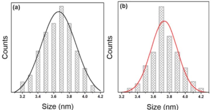
Colloidal PbS QDs and PbS@CdS QDs of diameters ranging between 2.9 - 4.1 nm were synthesized and then dispersed in toluene, with typical QY of 40 ~ 80%. We selected three different sizes of QDs: 3.0 ± 0.3 nm, 3.6 ± 0.3 nm, 4.0 ± 0.3 nm and compared pure PbS and PbS@CdS core@shell QDs with similar diameters (the representative size distribution for samples PbS_M and PbS@CdS_M are shown in Figure 3.1).
Figure 3.1 Size distributions of (a) PbS_M and (b) PbS@CdS_M QDs.
The absorption spectra of samples with different sizes of PbS and PbS@CdS QDs in toluene are shown in Figure 3.2 (a). The average PbS diameters for PbS QDs and the average PbS core size for the core@shell QDs are determined from the position of the first-lowest energy excitonic absorption peak (see Equation 1.1). [ 91 ] CdS shell thickness in PbS@CdS QDs can be obtained by simple subtraction from the overall size of PbS@CdS QDs based on TEM observations and the PbS core size. Based on previous achievements, [90] the shell of PbS@CdS QDs is mainly composed of CdS. The overall QD diameter (dtotal), core diameter (dcore), CdS shell thickness (dshell), the
Figure 3.2 Absorption spectra of (a) PbS and PbS@CdS QDs in solution. (b) Representative TEM image of PbS@CdS QDs. (c) EDX analysis of PbS@CdS QDs with ~3.0 nm
core diameter (shell thickness ~0.2 nm) after anchoring to TiO2 nanoparticles by
using EPD for 30 min (negative TiO2 electrode). Inset: SEM cross-section of a TiO2
film.
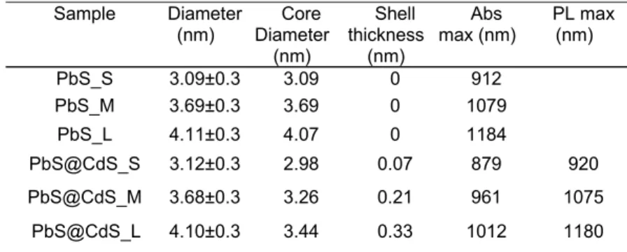
Table 3.1 Dimensions and optical properties of pure and core@shell QDs investigated in this
study. The overall size of PbS@CdS QDs is determined based on TEM observation, the core size is estimated from the position of the first excitonic peak and the shell thickness is estimated by simple subtraction. To identify the different samples, S M L labels are used according to their small, medium and large size, respectively.
Sample Diameter (nm) Diameter Core (nm) Shell thickness (nm) Abs max (nm) PL max (nm) PbS_S 3.09±0.3 3.09 0 912 PbS_M 3.69±0.3 3.69 0 1079 PbS_L 4.11±0.3 4.07 0 1184 PbS@CdS_S 3.12±0.3 2.98 0.07 879 920 PbS@CdS_M 3.68±0.3 3.26 0.21 961 1075 PbS@CdS_L 4.10±0.3 3.44 0.33 1012 1180
As-synthesized QDs were then loaded into mesoporous TiO2 layers through EPD.
TiO2 film thickness was around ~6 µm, estimated through stylus profilometer. SEM
the values between profilometry and SEM, which agreed within the experimental errors. After EPD of QDs, both the positive and negative TiO2 electrodes were colored (Figure
2.3 (b)), consistently with previous studies, [63, 78] indicating the deposition of negatively and positively charged QDs. According to literature, [92] the initial positive charge in nanocrystals can be understood in terms of the preferential removal of ligand, which exposes Pb (or Cd for core@shell) sites at the surface, which may also make QDs more “sticky” by reducing the solubilisation energy in the solvent, and may help charge transfer at the electrode surfaces. The origin of the negatively charged nanocrystals, can be explained with a S-rich surfaces or surface reconstruction upon the loss of the passivating ligand molecules, which exposes S atom. [93, 94] We investigated both positive and negative TiO2 electrode, presenting almost the same
results. Here we just show the investigation on negative TiO2 electrode. The effective
deposition of QDs into the TiO2 is confirmed by the EDX, Figure 3.2 (c)) in SEM (inset of
Figure 3.2 (c)), in which the signal from Cd, Pb and S are clearly visible.
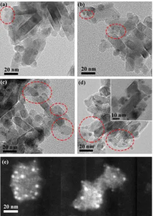
Figure 3.3 Representative TEM images of PbS@CdS QDs loaded into TiO2 at four different
min. Inset of (d): enlarged TEM image. The red circles highlight the presence of the
QDs. (e) Dark field Scanning TEM image of TiO2 nanoparticles covered by QDs. The
high contrast between the TiO2 and QDs allow precise identification of the position
of the QDs on the surface of TiO2 nanoparticles.
Figure 3.3 collects TEM images of negative TiO2 electrodes sensitized with
PbS@CdS core@shell QDs at different EPD durations. TiO2 coverage becomes denser
at increasing EPD time (Figure 3.3 (d)). In summary, the EPD process produces well-separated core@shell QDs, without obvious QD aggregation occurs, which could be detrimental for electron transfer in the operating device.
3.2 QD Stability after EPD
To check the effect of EPD on the stability of the structure and optical properties of QDs, we performed XPS and PL analyses of selected QDs deposited on silicon substrate or after EPD on TiO2 mesoporous films. We compared QDs with and without
CdS shell to test the ability of the shell to prevent QD degradation.
XPS was used to characterize the effect of EPD on the chemical bonds in QDs. The results are collected in Figure 3.4. The high-resolution spectrum of Pb 4f in PbS QDs on silicon reveals the presence of Pb 4f 7/2 (137.9 eV) and Pb 4f 5/2 (142.7 eV), respectively, from Pb-S bonds, and also two higher energy components (138.5 eV for Pb 4f 7/2 and 143.3 eV for Pb 4f 5/2), which can be originated from the interaction between Pb and OA ligands. [91] After EPD, the high energy peaks of Pb 4f totally disappear, and two additional lower energy components appear at 136.6 eV for Pb 4f 7/2 and 141.4 eV for Pb 4f 5/2 of PbS (Figure 3.4 (a)), which might be attributed to the presence of Pb dangling bonds due to the unpassivated Pb atoms on the QD surface, as a result of EPD. [91]The interaction between the QDs and TiO2 NPs might be the
reason for the shift of Pb-S bond to higher energies, from 137.9 eV to 138.1 eV for Pb 4f 7/2 and from 142.7 eV to 142.9 eV for Pb 4f 5/2. The high resolution spectrum of Pb 4f in PbS/CdS QDs on silicon (Figure 3.4 (b)) presents two additional higher binding energy peaks, similar to PbS QDs on silicon, slightly less intense than in PbS QDs. This feature possibly implies the presence of interaction between a small amount of unpassivated Pb atoms on the QD surface and ligands, as well as oxygen in aerobic
environments. In fact, some of PbS@CdS QDs might have an incomplete CdS shell, leaving some portion of Pb atoms at the surface. After EPD, in contrast to pure PbS, the two additional higher binding energy peaks almost maintained the same position as those on silicon, indicating increased damage in pure PbS QDs, while, for core@shell structure, there is no indication of formation of dangling bonds, and a relatively better structural stability.
Figure 3.4 High resolution Pb 4f core level spectra Photoelectron spectra after correction of
electrostatic charging obtained from (a) PbS_M quantum dot (b) PbS@CdS_M
core@shell quantum dot on silicon (up) and upload into TiO2 with EPD (down).
PL spectra of TiO2 samples after EPD of PbS and PbS@CdS QDs, 3.6 nm in size,
are reported in Figure 3.5 (a) and (b), respectively. Quantum confinement in QDs results in size-dependent band gap, inducing size dependent PL. The PL peak position
of pure PbS QDs after EPD (1175 nm) has a blue shift (32 nm) compared to pure PbS in solution (1207 nm), indicating the shrinking of QDs during uptake. After 24 hours exposure to air, the PL peak position further blue shifts (138 nm) compared to pure PbS QDs in solution, probably due to PbS oxidation. In fact, oxidation reduces the size of un-oxidized PbS, which is the source of PL, thus causing blue shift of PL signal due to the shrink of the emitting PbS volume. In addition, the peak width is quite broad (212 nm) with respect to that in solution (141 nm), indicating the presence of trap-related
emission, consistently with the presence of un-passivated dangling bonds confirmed by XPS (Figure 3.4 (a)). In PbS@CdS core@shell QDs, almost no shift of the PL peak was recorded, even after exposing the sample to air for 24 h (Figure 3.5 (b)), clearly demonstrating the increased optical stability thanks to the presence of the passivating shell.
Figure 3.5 PL of (a) PbS_M QDs and (b) PbS@CdS_M QDs just after EPD and after 24 hours
exposure to air. Benchmarking PL spectra of QDs in solution is also reported.
3.3 Dynamics of EPD
The increased stability of core@shell QDs motivated us to select this structure to investigate the dynamics of QDs uptaken during EPD. We applied RBS to get information on depth profiling of QDs inside the TiO2 matrix. The RBS spectrum of a
Figure 3.6 (a) RBS spectrum of TiO2 mesoporous film sensitized with QDs for 120 minutes.
The red curve is the RUMP code simulation. The surface edges for Ti, Cd and Pb are indicated by arrows. (b) RBS signal of the spectral region pertaining Pb signal for samples sensitized at different durations (5, 10, 30, 60, 120 minutes, from dark blue to light azure). A and B rectangles highlight the two different regions in which QD diffusion cannot be detected (A) or is clearly visible (B).
The signals from Ti and Pb are clearly visible, allowing quantitative analysis of in-depth distribution of Pb into the TiO2 layer. The red curve is the RUMP code simulation,
including also the contribution from FTO substrate, demonstrating that very accurate depth profiling of Pb is possible in this kind of samples. The signal from Cd is masked by Pb, can be hardly detected, and is very close to the detection limit of the technique in the present experimental conditions. For this reason, we focused on the depth profiling of Pb, under the hypothesis that the core@shell structure and Pb:Cd atomic ratio is preserved after EPD and so, in principle, Cd depth profile is the same as Pb.
Figure 3.6 (b) focuses on the RBS spectral range related to Pb. Two different regions can be clearly identified: region A, relying with the inner part of the film at the TiO2/FTO
interface, and region B, which represents the exterior part of the film, close to the
300 400 500 600 700 575 600 625 650 675 700 Ti Pb yield (a.u.) channel (a) Cd B (b) yi el d (a.u. ) channel surface A 0.0 0.5 1.0 1.5 2.0 Pb concentration (at. %) 5 4 3 2 1 0 depth (m)
surface. In region A, the concentration of Pb is almost constant and depth-independent, and increases exponentially with EPD time (see Figure 3.7).
Figure 3.7 Pb atomic ration as a function of EPD time at the interface of TiO2/FTO for PbS@
CdS_L (red line) Black line corresponding to the change of the curvature.
Pb is present even at very short EPD time, indicating that the solution containing QDs penetrates the entire film depth from the beginning of the process and that QD start attaching to TiO2 over the entire depth of the film. In region B, a surface Pb peak is
present after 5 min EPD deposition. Then Pb penetrates the film during EPD. Pb surface concentration increases with the time up to a saturation concentration (see Figure 3.8).
Figure 3.8 Pb atomic ration as a function of EPD time at the surface of TiO2 film of
PbS@CdS_L 0 20 40 60 80 100 120 0.0 0.1 0.2 0.3 0.4 0.5 0.6 0.7 0.8 Pb at. % time (min) 0.0 0.2 0.4 0.6 0.8 1.0 n (a.u.) 0 20 40 60 80 100 120 0.0 0.5 1.0 1.5 P b fr o nt ( a t. % ) t (min)


![Figure 1.3 The equivalent circuit of a solar cell. [32]](https://thumb-eu.123doks.com/thumbv2/123doknet/5395837.125570/19.892.293.621.153.343/figure-equivalent-circuit-solar-cell.webp)
![Figure 1.4 Getting the important parameters From the I-V Sweep.[34]](https://thumb-eu.123doks.com/thumbv2/123doknet/5395837.125570/20.892.263.635.155.411/figure-getting-important-parameters-i-v-sweep.webp)

![Figure 2.1 Image showing the air-free reaction setup for synthesizing PbS QDs. [90]](https://thumb-eu.123doks.com/thumbv2/123doknet/5395837.125570/28.892.291.607.162.412/figure-image-showing-free-reaction-setup-synthesizing-pbs.webp)