Université du Québec
Institut National de la Recherche Scientifique Centre Énergie Matériaux Télécommunications
On-surface formation of graphene-like materials through Ullmann coupling
Par
Galeotti Gianluca
Mémoire ou thèse présentée pour l’obtention du grade de Philosophiae doctor (Ph.D.)
en sciences de l’énergie et des matériaux
Jury d’évaluation
Président du jury et Emanuele Orgiu
examinateur interne INRS-EMT
Examinateur externe Fabio Cicoira
Département de Génie Chimique Polytechnique Montréal
Examinateur externe James D. Wuest
Département de Chimie Université de Montréal
Directeur de recherche Federico Rosei
INRS-EMT
DEDICATION
To my family, to Federica and to those who are in my heart
«All truths are easy to understand once they are discovered; the point is to discover them»
ACKNOWLEDGEMENTS
First of all, I would like to thank Federico, he proposed me this PhD, and he gave me scientific freedom. This was not due, and I appreciate it. I would also like to give a sincere thanks to Giorgio. He is the reason why I moved to Canada, and his impact on my career has been huge. Hopefully, I repaid their trust with this work. I would also like to thank Josh and Maryam, my day-to-day supervisors. Josh taught me to be a scientist, and to follow my curiosity. Maryam taught me to let my voice be heard in the scientific world and guided me through my first publication. Heartfelt thanks go to Mark, Sarah and Fabyola, who have ensured that this thesis was correctly written, both in English and in French
Being a researcher is a full-time job, and study surface science means to spend ludicrous amount of time in the lab. Therefore I would like to thanks all the people that worked with me and helped me during the periods of work at INRS (Fabrizio, Daniele, Luca, Mark, Riccardo, Stefano, Sarah, Jennifer, Daling, Penghui, Dominik) at CNR, Université de Lorraine, Tor Vergata and anyone who shared time and gave me an hand inside a lab. I would also like to thank all the other students from INRS. It has been an experience, I met amazing people from everywhere in the world and I will bring with me all those experiences.
A big thank you goes to all my friends. They are a reason to hold on and to live life with a positive attitude, so thanks to all my childhood friends, my friend from Montreal, and to all the friends who shared my university experience.
I would like to thank my family. My parents, ready to support me during good and bad times, and encouraging me to face the challenges of life. My brother and all the other relatives. A special thanks goes to Federica, with whom I am sharing my life, who knows anything of me and still loves me. Without you I do not know if I would have found the strength and motivation needed, you are simply too important for me.
In the end, I want to thank and remember all the people with whom I shared moments of my life but now are gone. I will bring them in my heart forever.
STATEMENT OF ORIGINALITY
The work presented herein has been performed in its integrity by the author during his PhD years. The experimental part of the thesis (Chapters 3 to 6) is based upon published works, in which the Author was either first author or part of the collaboration. The role of the Author in each work is reported at the beginning of the chapter, but it can be summarized as the following: all experimental procedures, from sample preparation and deposition to data analysis were developed or performed by the Author, sometimes in collaboration with other researchers (mostly Fabrizio De Marchi for STM experiments and Marco Di Giovannantonio for XPS and synchrotron beamline experiments). Theoretical calculations, namely DFT simulation and kinetic system modeling, have been performed by various collaborators, and the role of the author was to provide the initial structures or experimental data, apply the kinetic model to those data, and control the agreement of the calculations with the experimental results. The used molecular precursors were either bought from commercial sources or synthesized by collaborators from McGill University and Université Laval.
RÉSUMÉ
La réalisation de nano-dispositifs de quelques couches d'épaisseur est l'un des grands défis de la nanotechnologie. Cependant, le besoin de miniaturisation constante a introduit une nouvelle criticité qui pourrait casser l'équation électronique = silicium. Une solution possible pourrait être d'utiliser le graphène en tant qu'élément actif, car il s'agit d'un matériau naturel épais d'une couche possédant des propriétés optoélectroniques incroyables. Toutefois, l'inconvénient du graphène est sa bande interdite nulle, ce qui limite ses applications possibles. Cela a mené à l’étude de matériaux analogues au graphène, c’est-à-dire des polymères conjugués 1D et 2D aux propriétés accordables, développés par des approches ascendantes. L'objectif est d'utiliser les interactions molécule-molécule et molécule-molécule-substrat pour auto-assembler directement la structure souhaitée, ainsi que les manipuler pour obtenir un polymère étendu doté de la bonne architecture et de possibilités d’adaptation. Les réactions en surface sont une voie alternative à la réaction en solution, qui est l’approche habituellement utilisée pour obtenir la structure polymérique souhaitée. La présence de la surface permet de contrôler la dimensionnalité et de réaliser des réseaux 1D et 2D, tout en participant à la réaction en tant que source d’adatomes ou en jouant le rôle de catalyseur, abaissant les barrières d’énergie. Des nouvelles et intéressantes voies de réaction sont offertes par la surface, où des réactifs insolubles pourraient également être impliqués, mais une connaissance et un contrôle précis de tous les paramètres de réaction – en particulier des interactions critiques substrat-molécules – sont nécessaires pour exprimer pleinement le potentiel de cette approche. Dans cette thèse, nous explorerons les réactions en surface utilisées pour obtenir des polymères conjugués, en nous concentrant sur la réaction de couplage de Ullmann, tout en donnant des informations générales sur d'autres approches, telles que la polymérisation du diacétylène. Le couplage Ullmann en surface est la réaction la plus utilisée – et la plus efficace – pour la préparation ascendante de polymères conjugués 1D et 2D sur des substrats métalliques, avec des propriétés adaptées au choix du précurseur moléculaire. Celui-ci est établi comme le moyen principal de réaliser des matériaux analogues au graphène, c’est-à-dire des feuilles de graphène avec un taux de trame élevé ou avec une présence ordonnée d’hétéroatomes ou de lacunes. En combinant des techniques morphologiques (microscopie à effet tunnel) et compositionnelles (spectroscopie par photoémission), étayées par des modélisation théoriques (théorie de la densité fonctionnelle), nous avons exploré les paramètres de réaction afin de mieux comprendre le mécanisme réactionnel et
la cinétique: l'effet de la couverture, de l'halogène, de la surface et des hétéroatomes soufrés ont été étudiés. Les résultats ont été mis en perspective pour permettre de mieux comprendre la formation de matériaux de l’ordre de la longue distance analogues au graphène .
Mots-clés: Science des surfaces, Polymérisation à la surface, Couplage Ullmann, Matériaux
analogues au graphène, STM, XPS, Fast-XPS
ABSTRACT
The realization of few-layer thick nano-devices is one of the great challenges of nanotechnology. The need for constant miniaturization has however introduced new challenges that may break the electronics = silicon equation. A possible solution could be to use graphene as an active element, since it is a natural one-layer thick material with incredible opto-electronic properties. The downside of graphene is however its zero bandgap, which limits its possible applications. This led to the study of graphene-like materials, i.e. 1D and 2D conjugated polymers with tunable properties, grown through bottom-up approaches. The goal is to use molecule-molecule and molecule-substrate interactions to directly self-assemble the desired structure, and to further manipulate them into extended polymers with the correct architecture and tailoring possibilities.
On-surface reactions are an alternative route to the common solution-based approach to obtain the required polymeric structure. The presence of the surface enables control of the dimensionality, constrains the growth and allows realization of 1D and 2D networks, while at the same time participating in the reaction as a source of adatoms or working as a catalyst, lowering energy barriers. New and interesting reaction pathways are enabled by the surface, in which insoluble reagents can also be involved, but a precise knowledge and control of all the reaction parameters – in particular of the critical surface-molecule interactions – is necessary to fully convey the potential of this approach. In this thesis we will explore the on-surface reactions used to obtain conjugated polymers. The main focus will be on the Ullmann coupling reaction, but general information will be given on other approaches, such as diacetylene polymerization.
On-surface Ullmann coupling is the most used – and successful – reaction for the bottom-up preparation of 1D and 2D conjugated polymers on metallic substrates, with properties tailored by the choice of molecular precursor. It is established as the main way to realize graphene-like materials, i.e. graphene sheets with a high aspect ratio (e.g. nanoribbons) or with the ordered presence of heteroatoms or vacancies (e.g. porous graphene). By using a combination of morphological (scanning tunneling microscopy) and compositional (photoemission spectroscopy) techniques, supported by theoretical modeling (density functional theory), we explored the reaction parameters, to improve the understanding of the reaction mechanism and kinetics: the effect of the coverage, of the choice of halogen, of the surface and of including sulphur heteroatoms. The results were put into perspective to gain insight into the formation of long-range ordered graphene-like materials.
Keywords: Surface science, On-surface polymerization, Ullmann coupling, graphene-like
TABLE OF CONTENTS
1 INTRODUCTION... 17 1.1 MOORE’S LAW... 20 1.2 ORGANIC ELECTRONICS ... 22 1.3 GRAPHENE ... 24 1.3.1 GRAPHENE FABRICATION ... 251.3.2 GRAPHENE, NANOMATERIALS AND TRANSISTORS ... 25
1.3.3 GRAPHENE MODIFICATION ... 27
1.3.4 2D POLYMERS:ORGANIC ANALOGUE OF GRAPHENE ... 29
1.4 SURFACE VS SOLUTION POLYMERIZATION ... 30
1.4.1 ADSORPTION ON SOLID SURFACES ... 32
1.5 ON-SURFACE POLYMERIZATION ... 34
1.5.1 ULLMANN REACTION ... 35
1.5.2 ON-SURFACE ULLMANN REACTION: PROPERTIES AND PRODUCTS ... 37
1.5.3 OTHER ON-SURFACE REACTIONS ... 53
2 THEORY AND EXPERIMENTAL METHODS ... 55
2.1 SCANNING TUNNELING MICROSCOPE ... 55
2.1.1 BASIC PRINCIPLE ... 56
2.1.2 BARDEEN METAL-INSULATOR-METAL MODEL ... 58
2.1.3 STM OPERATION MODES ... 60
2.2 X-RAY PHOTOELECTRON SPECTROSCOPY ... 62
2.3 SYNCHROTRON LIGHT-SOURCE FACILITY ... 64
2.3.1 FAST-XPS ... 66
2.3.2 ANGLE RESOLVED PHOTOEMISSION SPECTROSCOPY ... 66
2.3.3 NEAR-EDGE X-RAY ABSORPTION FINE STRUCTURE SPECTROSCOPY ... 69
2.4 PRECURSORS INVESTIGATED ... 72
3 THE COMPLEXITY OF A SIMPLE SYSTEM : THE CASE OF DBB ON CU(110)... 75
3.1 INTRODUCTION ... 75
3.1.1 MATERIALS AND METHODS NOTE ... 76
3.2 RESULTS AND DISCUSSION ... 77
3.2.1 REACTION KINETIC FOR DBB/CU(110) AT 1ML ... 77
3.2.3 EFFECT OF THE COVERAGE – A NEW INTERMEDIATE OF THE ULLMANN COUPLING ... 85
3.2.4 REACTION KINETIC FOR DBB/CU(110) AT 0.5ML ... 92
3.3 CONCLUSIONS AND PERSPECTIVES ... 93
4 A SYSTEMATIC STUDY : HOW TO INFER THE ROLE OF THE HALOGENS ... 94
4.1 INTRODUCTION ... 94
4.2 MATERIALS AND METHODS NOTES ... 95
4.3 RESULTS AND DISCUSSION ... 95
4.3.1 FAST-XPS AND REACTION OVERVIEW ... 95
4.3.2 STRUCTURAL CHARACTERIZATION BY STM ... 102
4.3.3 NEXAFS AND MOLECULAR ORIENTATION ... 106
4.3.4 ROLE OF THE HALOGEN IN THE REACTION ... 107
4.4 CONCLUSIONS AND PERSPECTIVES ... 109
5 FROM 1D TO 2D: CAN WE MAKE GRAPHENE-LIKE MATERIALS? ... 111
5.1 INTRODUCTION ... 111
5.2 RESULTS AND DISCUSSION ... 112
5.2.1 TBTTB ON AU(111) ... 112
5.2.2 TBTTB ON AG(111) ... 116
5.2.3 TBTTB ON CU(111) ... 120
5.2.4 SURFACE COMPARISON ... 121
5.3 CONCLUSIONS AND PERSPECTIVES ... 122
6 DIFFERENT ROUTES FOR ON-SURFACE POLYMERIZATION: ACETYLENE-ACETYLENE COUPLING ... 124
6.1 INTRODUCTION ... 124
6.2 RESULTS AND DISCUSSION ... 126
6.2.1 STM DATA &DFT CALCULATIONS ... 126
6.2.2 XPS AND TEMPERATURE-DEPENDENT MULTILAYER STABILITY ... 132
6.2.3 HYDROGEN BONDING HINDERS TOPOCHEMICAL POLYMERIZATION ON THE SURFACE ... 134
6.3 CONCLUSIONS AND PERSPECTIVES ... 136
7 CONCLUSIONS AND PERSPECTIVES ... 137
7.1 FUTURE STUDIES... 140
7.2 ORDER OF THE STRUCTURES ... 142
7.3 GOING REAL: HOW TO INCORPORATE GRAPHENE-LIKE MATERIALS INTO A DEVICE ... 146
7.3.1 A GRAPHENE NANORIBBONS TRANSISTOR ... 146
8 RÉSUMÉ ... 149
8.1 INTRODUCTION ... 149
8.1.1 POLYMÉRISATION EN SURFACE ... 152
8.1.2 MICROSCOPE À EFFET TUNNEL ... 156
8.1.3 SPECTROMÉTRIE DE PHOTOÉMISSION INDUITS PAR RAYONS X ... 157
8.1.4 PRÉCURSEURS UTILISÉS ... 159
8.2 RÉSULTATS ET DISCUSSIONS ... 160
8.2.1 DBB/CU(110)–EFFET DU TAUX DE RECOUVREMENT ... 161
8.2.2 DBB/CU(110) HAUT TAUX DE RECOUVREMENT : CINÉTIQUE DE LA RÉACTION ... 162
8.2.3 DBB/CU(110) FAIBLE COUVERTURE : ÉTAT INTERMÉDIAIRE TRANSITOIRE ... 164
8.2.4 DI-HALOBENZENES ON CU(110)–EFFET DE L’HALOGÈNE ... 165
8.2.5 EFFET DE LA SURFACE ... 166
8.2.6 DÉPÔT À CHAUD –RÉSEAUX ORGANOMÉTALLIQUES ORDONNÉS DE TBTTB ... 167
8.3 CONCLUSIONS ET PERSPECTIVES ... 168
8.3.1 ETUDES FUTURES ... 170
LIST OF ACRONYMS
a-Si – amorphous silicon
AES – Auger electron spectroscopy AEY – Auger electron yield
Ar-X – aryl halides
ARPES – angle-resolved photoelectron spectroscopy BCB – 1,4-bromoclorobenzene
BE – binding energy CNTs – carbon nanotubes CCM – Constant Current Mode CHM – Constant Height Mode
CMOS – complementary metal-oxide semiconductor CVD – thermal chemical vapor deposition
DBDA – di-benzonitrile-diacetylene dCB – 1,4-dichlorobenzene
dBB – 1,4-dibromobenzene dIB – 1,4-diiodobenzene
DFT – density functional theory DOS – density of states
FET – field-effect transistors finFETs – fin field-effect transistor GNRs – graphene nanoribbons
HOCO – highest occupied crystal orbital
HOPG – highly oriented pyrolytic graphite samples
HREELS – high resolution electron energy loss spectroscopy IBB – 1,4-iodobromobenzene
IntS – intermediate state
LEED – low-energy electron diffraction LUCO – lowest unoccupied crystal orbital MOF – metal-organic framework
NEXAFS – near edge X-ray absorption fine structure OM – organometallic
OLED – organic light-emitting diodes OFET – organic field-effect transistors PEY – partial electron yield
PPP – poly-para-phenylene
SAMs – self-assembled monolayers SET - single-electron transfer
SiO2 – Silicon dioxide
SR – synchrotron radiation
STM – scanning tunneling microscopy STS – scanning tunneling spectroscopy TBB – 1,3,5-tris(4-bromophenyl)benzene TEY – total electron yield
TIB – 1,3,5-tris(4-iodophenyl)benzene TBTANG – tribromo-triangulene TBTTB – tribromo-terthienobenzene TFTs – thin-film transistors
TMDs – transition metal dichalcogenides UHV – ultra-high vacuum
1
INTRODUCTION
Over the last several years, there has been a tremendous effort to develop new and innovative solutions that could revolutionize device design and fabrication.1 This is due to the fact that silicon-based technology, though it has driven the semiconductor industry until now, could soon become unable to offer the ever-increasing need for constant miniaturization at the same time as improved device performance.2-4 Therefore, a natural solution is to undertake a fundamental change, moving from the seemingly “doomed” silicon technology to something different, but the transition involves considerable challenges. For example, the isolation of graphene5 and its development in the last decade has given rise to rejuvenated interest in carbon-based electronics. This interest is easily explained by the remarkable properties of this material6-7 such as astonishingly-high thermal and electrical conductivity. Such properties can be exploited in various applications, from transistors,8 to gas9 (or even isotope10) separation, to nano-devices.11 This is surprising for a material that based on thermodynamic considerations by Landau and others should not even exist.12-13 Despite its unique properties, graphene’s zero electronic bandgap limits its application
in electronics. Recent studies have addressed this problem and tried to suggest some solutions,14
however an easy and repeatable process to achieve this is still missing.
The flexibility of organic synthesis offers a broad playground to create organic analogues of graphene with high charge mobility and tunable bandgaps. Among organic materials, polymers can be commonly obtained through bottom-up building methods which result in small ordered structures. Therefore, instead of making graphene and then trying to modify it, a different and maybe more promising approach would be the bottom-up realization of different two-dimensional (2D) polymer analogues to graphene, with a different geometry in which heteroatoms could be incorporated. The idea is to identify processes that can couple small organic molecules into 2D polymers, where the building blocks can be chosen based on the desired properties. This a priori step could be performed using ab initio calculations.15 It should be noted that in solution, polymers tend to fold and roll up, and to avoid this a possible solution is to constrain the growth on a surface, obtaining 1D or 2D polymers. The substrate can also be used as a catalyst, lowering energetic barriers and further guiding the reaction.16 The result would be conjugated polymers with electronic band structures similar to that of graphene but with different properties (e.g. charge-carrier transport velocity and Fermi velocity) and an adjustable bandgap.
Figure 1-1 Scheme of the necessary steps to realize devices using on-surface polymerization; a) the selected building block is chosen; b) it is dosed onto a surface where it reacts to form 2D polymers; at this point it can either be detached from the surface (c), or the underlying surface can be modified to obtain a working device (d).
The whole process needed to realize practical devices starting from simple molecules is shown in Figure 1-1, which can be described as the take-away message of this thesis. From the pioneering works of Okawa and Aono,17 most of the effort have been put into finding the right monomers and controlling the polymerization reaction,18 which can result in the formation of 1D19 and 2D20 polymers. Accordingly many different reactions have been studied, such as polycondensation, Glaser Hay and Sonogashira coupling.21-23 Once made, the properties of these materials will depend on the density of defects,24 and therefore the chemical purity and the structural order are essential parameters to take into account for these systems. Although it is relatively easy to obtain long-range ordered molecular self-assembled monolayers (SAMs) on surfaces, such a level of order has not been achieved for covalently-bonded structures. The reversible nature of the intermolecular forces in a SAM yields enough surface mobility to the molecules to reach a minimum energy geometry, and results in large ordered domains. A possible approach to form long-range ordered covalent structures is to use a multi-step reaction, in which
the molecules would arrange in such a way that the functional groups of the neighboring molecules can easily and efficiently interact. This step can then guide the formation of irreversible covalent bonds into the final ordered structure or network.15, 25
One of the most common reactions that expresses these features is Ullmann coupling, a two-step reaction which exploits the catalytic activity of a supporting transition metal substrate,26 to de-halogenate aryl halide precursors, and subsequently couple the radicals into polymers.27 Both steps are temperature dependent,16 with the activation energy depending on the molecule28 and the surface.29 In most cases, the obtained structure after deposition on noble metal surfaces is an organometallic (OM) compound, the intermediate of the reaction that is stable up to the polymerization temperature.30-31 Since the first report of an on-surface Ullmann reaction,32 various groups tried to gain insight into the reaction mechanism and kinetics,26-27, 33 however, we can safely state that, even after a decade of study, there are still open questions about these systems, regarding both the fundamental understanding and the practical realization of the process.34
The work presented in this thesis is focused on studying these questions, both from a fundamental point of view, studying the role of the halogen and the reaction mechanism of simple molecules (Chapters 3-4), and a practical perspective, guiding the reader through the difficulties of forming a two-dimensional organic structure (Chapter 5). Chapter 6 will explore instead a different way to realize polymeric structures on a surface, namely diacetylene polymerization. The first two chapters will focus on the knowledge necessary to grasp the experimental results, with
Chapter 1 describing to the reader the “why” of the research and Chapter 2 focusing on the
“how”. The concluding Chapter 7 will give an overview of the results obtained, how they fit within the existing literature, and how they could be further expanded and improved. Chapter 8 will provide a summary of the thesis background and results for the French readers, while Chapter
1.1
Moore’s Law
Since the invention of the transistor in 1947, electronics has driven technological innovation, in what can be described as a historical revolution as important as the industrial revolution of the 18th century. Electronics is now fundamental to almost every device we use and most aspects of our life, to the point where it is quite hard to think about working, connecting with other people, or even spending one day without being affected by it.
The most impressive feat of this revolution is the remarkable speed with which it proceeded, to the point that nowadays a common chip made of billions of transistors has a size of a few millimeters. This rate of reduction in the transistor’s size and cost was predicted by Gordon Moore in an article he wrote for Electronics Magazine.35 Moore predicted that for each new generation of memory chip and microprocessor unit on the market, the device size would reduce by 33%, the chip size would increase by 50%, and the number of components on a chip would quadruple every three years.2 This prediction has been valid for more than 50 years, and the
technology industry still expects to follow an exponential increase in complexity of integrated circuits. However, as Greg Yerig, director of future silicon technology for ARM Research, said in 2017: “past progress in Moore’s law has been achieved by implementing the easy ones. Now we are faced with more difficult choices”.36
At the moment, the further scaling of transistors faces various problems from fundamental issues, such as the Abbe diffraction limit for photolithography or the Amdahl limit for parallel processing, to more specific ones related to device architecture and materials properties, such as the carrier mobility, gate oxide thickness, current leakage or cross-talk, and many more.37-39 One of the main problems that will need to be addressed is the oxide gate thickness.2 Silicon dioxide (SiO2) is an almost perfect insulator with a resistivity higher than 1016 Ω×cm. The
insulating SiO2 films grown on silicon are smooth and coherent, with no holes in a thickness range
down to few atomic layers,40 and only a few electrically active defects at the interface.41 Such thin films are required to maintain the current response of the transistor to lower voltages at the gate electrode. But reducing the transistor size will require a reduction in the oxide thickness, and, as Figure 1-2 shows, such reduction will mean that parasitic resistance could become comparable to, or even exceed, the channel resistance.
Figure 1-2 a) evolution of the gate length for planar MOSFET up to the year 2020, and b) graph of the corresponding channel resistance vs the gate size. A limit for the gate size is obtained when the parasitic resistance dominates over the channel resistance. Adapted from Ref.42
With Si complementary metal-oxide semiconductor (CMOS) scaling limits in sight, the obvious questions are “What nanotechnology is on the horizon to replace planar Si CMOS transistors and in what time frame can this happen?”.36 Though these are difficult and perhaps foolhardy questions to try and answer, it is important to attempt to do so since this affects a $330 billion worldwide industry and the careers of many engineers.43 It is clear however that, to follow Moore’s exponential growth, new ideas or even a change of paradigm are necessary.
1.2
Organic electronics
Solving the Si scaling problem is going to be challenging, and while some attempts have already been made to extend silicon life (such as multi chip technologies, or even changing the chip architecture by introducing the fin field-effect transistor (finFETs)),44-45 one of the solutions could be breaking the electronics = silicon equation. A possible new player in this arena could be found in organic materials. Organic molecules have in fact been used as active components in electronic devices for years,46 and their use continues to grow, guided both by the promise of cost reduction and by the possibility of introducing new features.47 A practical example of this can be found in organic light-emitting diodes (OLED) for displays, which can be printed on lightweight and even flexible/foldable plastic substrates.48
The first report of organic conductive materials traces back to the work of Heeger, MacDiarmid and Shirakawa in the ‘70s, when they found that polyacetylene could become highly electrically conducting after undergoing a structural modification.49-50 They observed an increase
in the electrical conductivity of the materials by orders of magnitude after exposing it to vapors of I2. The I2, which is an electron acceptor compound, was abstracting electrons from the polymer,
hence doping it. The same effect was shown also for Cl2, Br2 and AsF5, which are all p-type
dopants. The conductivity is believed to be a result of the creation of charge-transfer complexes between the polymer and the halogens and is preserved even after exposing the material to air for several days. Heeger, MacDiarmid and Shirakawa’s work started a prolific field of research, which led to the development of organic field-effect transistors (OFET)51 and was later recognized by awarding them the 2000 Nobel prize in Chemistry.
The polyacetylene used in their studies is part of a class of polymers called conjugated polymers. This conjugation refers to the alternation between single and double (or triple) bonds, so that all carbon atoms in the backbone have sp2 (or sp) hybridization.52 This hybridization allows for delocalization through the whole system, so that the electrons are free to move and become charge carriers, making the polymer conductive.52 The electrons in these delocalized orbitals have higher mobility when the material is “doped”, i.e. oxidized. The oxidation removes electrons from the one-dimensional electronic band, which becomes partially empty, enabling the electrons within the band to become mobile. In principle, the same effect can be obtained by reduction, which adds electrons to an unoccupied band. Examples of n-type dopants are lithium, sodium and potassium.
However, most organic conductors are doped oxidatively (i.e. p-type materials), and n-type doped materials are more sensitive to air and moisture. The doping of such organic conductors can be seen as an analogue to the doping of semiconducting silicon. The band structures of conductive polymers can easily be calculated using a tight binding approach. Conjugated polymers can exhibit metallic or semiconducting behavior and their electrical properties can be tuned by modifying the structure of molecules. This is of crucial importance because the tunability enables these materials to be used as active components in multiple devices for different applications.53-55
Figure 1-3 a) benzene molecule with the C 2pz orbitals drawn in red; b) drawing of the delocalization of
the charge density above and below the benzene ring plane; c) schematic of a longer molecule (beta-carotene) with the conjugated carbon backbone highlighted in red. a,b) Adapted from Ref.56 CC BY-SA 3.0
1.3
Graphene
A significant leap towards the usage of organic electronics beyond niche applications was spurred by the isolation of graphene in 2004 by Geim and Novoselov, for which they were granted the Nobel prize shortly afterwards.57 Graphene is an allotrope of carbon whose structure is a single planar sheet of sp2 bonded carbon atoms, that are densely packed in a honeycomb crystal lattice.58
Figure 1-4 Graphical representation of a graphene single layer. Reproduced from Ref.59 CC
BY-SA 3.0
The interest in graphene lies in its unique properties.6-7 It is a zero-gap semimetal, with a
linear E vs k relation for low energies near the six corners of the two-dimensional hexagonal Brillouin zone, where cone-like structures, called Dirac cones, are formed.6 Charge transport
measurements show that graphene charge carriers are massless Dirac fermions,60 which is reflected
in astonishingly high thermal and electrical conductivity. The properties would make graphene a perfect component for integrated circuits, but its usage has been limited by two main factors: i. single sheets of graphene are remarkably hard to produce, particularly on top of substrates appropriate for device fabrication and ii. the zero bandgap. The first problem was solved by transferring graphene layers from the growth substrate to destination substrates, while the latter issue is yet to be solved, and the work in this thesis is an attempt at a solution.
1.3.1 Graphene fabrication
Graphene was first isolated and identified in 2004, but existed in nature as a single layer in graphite, and was already studied in the ‘70s. In 1975, B. Lang synthesized a few-layer graphite sample via chemical decomposition methods on a single crystal platinum surface.61 Epitaxial growth on transition metals was fairly common during the ‘70s,62 but it was only with the advancement of surface science, in particular with the more widespread use of techniques such as low-energy electron diffraction (LEED), Auger electron spectroscopy (AES), high resolution electron energy loss spectroscopy (HREELS) and scanning tunneling microscopy (STM) that real progress was made, and single-to-few layer graphene flakes were obtained on SiO2 by
mechanically exfoliating highly oriented pyrolytic graphite samples (HOPG).63 After the work of
Geim and Novoselov6, 58 the interest in graphene skyrocketed, and nowadays there are multiple ways to reliably synthesize graphene: mechanical cleaving (exfoliation),57 chemical exfoliation,64
chemical synthesis,65 thermal chemical vapor deposition (CVD),66 unzipping nanotubes67 and microwave synthesis.68 A graphical representation of those techniques is reported in Figure 1-5.
Figure 1-5 Process flow chart of various graphene synthesis techniques. Reproduced from ref.69-70, CC
BY-SA 4.0
1.3.2 Graphene, nanomaterials and transistors
While high-performance microprocessors based on MOSFETs are what we commonly refer to when we speak about current technology, numerous applications do not require the use of high cost MOSFETs, such as optical detectors, chemical sensors and even pixel-driving circuits for
displays.43 The backplane electronics of flat panel displays are in fact the most prominent use of
transistors aside from in microprocessors, and use low-cost amorphous silicon (a-Si) thin-film transistors (TFTs). Such TFTs have a lower requirement for performance and size but need to be lower-cost, and could therefore be the right market niche for graphene transistors.43, 71 An important aspect of graphene transistors, or more generally of nanomaterial transistors, is that the device architecture is pretty similar for high-performance and thin film transistors (Figure 1-6a).43
Figure 1-6 a) Cross-sectional schematics showing the general structure of high-performance and thin film transistors using nanomaterials for the channels; there are small differences in the structure but vast differences in size; b-c) overview of benefits and challenges of including nanomaterials into transistors; d) comparison of key intrinsic attributes between silicon and the four most prominent families of nanomaterials. Adapted from Ref.43 with permission from
The American Association for the Advancement of Science.
Apart from graphene, other nanomaterials could be used, such as carbon nanotubes (CNTs), transition metal dichalcogenides (TMDs) and the class of X-ene 2D materials, i.e. silicene and phosphorene (Figure 1-6). Using nanomaterials as channels would provide a number of
benefits, the first being thinness. The atomic thinness of nanomaterials, especially in their monolayer form, offers ideal electrostatic control over the channel, one of the main problems with further downscaling in the size of Si transistors. 2D materials could also be stacked, to modify their properties, and could be synthetized on one particular substrate and then transferred onto the device. As of now, however, there are huge challenges to overcome before nanomaterials offer a real alternative to silicon, such as producing high-quality materials, controlling their placement onto a device, and the need to improve the interfaces (contact and dielectric) and device architectures, to fully utilize their advantages (Figure 1-6b,c).43 Finally, in Figure 1-6d I show an overview of the key intrinsic attributes of the four families of nanomaterials and compare them with silicon. While graphene clearly shows the best properties, as highlighted before, the main drawback is the zero bandgap, which hinders its application as a semiconductor.
1.3.3 Graphene modification
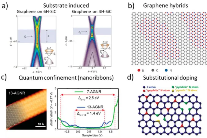
For most applications in electronics, a bandgap and the ability to tune its value is required, meaning that finding a way to reliably and easily modify the bandgap of graphene will have a tremendous technological impact. The carbon atoms in the single atomic sheet are sp2 hybridized and each atom has an unsaturated dangling bond, making it possible to perform various surface modifications. There are different ways to tackle the problem, and the most common are: i. substrate-induced bandgap opening, ii. substitutional doping, iii. BCN hybrids and iv. quantum confinement (Figure 1-7). Substrate-induced bandgap opening was the first method explored, and interestingly was reported for the first time a few years before the work of Geim and Novoselov. In 2002 a graphene/h-BN/Ni (111) system was studied by scanning tunneling spectroscopy (STS), showing a 0.5 eV bandgap, thus confirming a gap opening.72 The method has been widely used since and has been demonstrated also for adsorbed molecules73 and even hydrogen.74 Chemical substitution doping is conceptually similar to conventional semiconductor doping, and consists of substituting carbon atoms with either boron or nitrogen to obtain n- or p-type semiconductors, respectively. However, it is still in the early stages of development, and obtaining uniform doping over large areas of graphene remains a challenge.69 Hybrids consist of BCN solid solutions in a
to work with distinct layers of graphene and h-BN systems. A major drawback of the previous methods is that the carrier mobility was reduced by the graphene modification, thus affecting the device performance. One way to avoid such a problem while introducing a gap is to confine the electrons in graphene by making graphene nanoribbons (GNRs).75 As I will present in Section 1.5.2, on-surface polymerization has been shown to be a reliable way to produce GNRs, and some experimental results on this aspect will be discussed in Chapter 3. Studies on Graphene modification are ongoing, and an increasing number of scientists and associated laboratories are starting to venture into such modification. A new class of graphene-like materials was also proposed, 2D π-conjugated polymers, whose properties are defined by the precursors, and easier to tune, being defined by the used monomer.
Figure 1-7 Schematic of various methods of bandgap opening in graphene. Reproduced with permission
1.3.4 2D polymers: Organic analogues of graphene
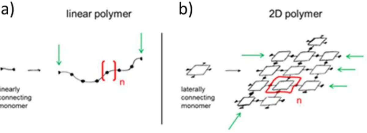
Figure 1-8 Graphical representation of the formation of linear (a) and 2D (b) polymers starting from their building blocks. Adapted from Ref.80 CC BY-SA 3.0
According to Hermann Staudinger’s definition from the 1920s, a polymer is a covalent long-chain molecule composed of a sequence of linearly-connected repeating units and end groups.81 A sheet-like macromolecule of connected repeating units, such as graphene. can be defined as a 2D polymer.Graphene is therefore the simplest example of a 2D polymer, with only carbon atoms as the repeat unit, but it is possible to imagine a whole class of polymers with different properties and characteristics, depending on the initial building block used. The final result can include heteroatoms and have different geometries, as shown in Figure 1-9.
Thus, it would be possible to change both the physical (such as optical and electrical) and chemical (such as reactive) properties of the obtained layer, including the aforementioned bandgap. Such modifications will open paths to whole new classes of applications, such as chemical sensors or active optoelectronic components, which explains the increasing interest in this field.15, 82 The macromolecular nature of these materials provides a great number of degrees of freedom, through the choice of monomer geometry and composition as well as the co-deposition of different monomers.
Figure 1-9 Scheme of the relation between the precursor halogen functionalization and the dimensionality and topology of the resulting polymeric network. Reproduced from Ref.34 With
permission of The Royal Society of Chemistry.
1.4
Surface vs Solution polymerization
In the introduction, I stated that to realize our 2D structures it is necessary to dose the precursors on top of a surface, let them assemble, and react directly on the substrate. But why is it necessary? In other words, could this whole process be done using a more traditional solution-based chemistry approach? The short answer of course is that yes, the surface is necessary, since the realization of dimension-limited polymeric structures in solution will pose almost insurmountable difficulties.However, the causes of these difficulties are subtle and worth discussing, to let the willing reader understand the perspectives of this on-surface approach and its advantages and its drawbacks compared with the more common solution-polymerization approach. In the previous sections I introduced 2D materials, including graphene and organic polymers, but before 2004 they were considered impossible to create, and merely useful as models for theoreticians to better understand solid state physics. Graphene has been studied theoretically for almost 60 years and was believed to be a highly unstable material, but now you can buy a 50 mL solution of graphene flakes for less than $50, so the question arises: how is this even possible?
The idea of unstable 2D systems arose in the 30s with the work of Peierls,83 who, based on
the harmonic approximation, showed that there can be no one- or two-dimensional long-range order. (To be more accurate, he gave a quantitative argument only for the 1D case but showed the obvious connection to two dimensions). An independent proof was found a few years later (in 1937) by Landau, using his general theory of second-order phase transitions.84 Those arguments were later extended by Mermin, in 1968,85 who studied the case of N classical particles interacting through a pair potential in two dimensions. Using the Bogoliubov inequality (that satisfies the free energy of a Hamiltonian system), he found that conventional crystalline order in two dimensions is forbidden for Lennard-Jones type potentials.85 The reason is that there is a divergence in the displacement autocorrelation function, and so positional long-range order does not exist.85 However, he found weaker bounds than those found by Peierls with the harmonic approximation, and stated that short-range order could still exist. Essentially, the divergence can be seen as a divergent contribution of thermal fluctuations, which means that at any finite temperature the atom displacement is comparable to interatomic distance, and so there is no ordering (basically, the crystal melts). This was also supported by experimental observations, which stated that the melting temperature of thin films is directly proportional to the thickness of the films, and that thin layers will have low melting points.86-87 However, in 2004 Geim and Novoselov isolated and studied a
single layer of graphene,57 and the problem, thought to be closed since the 60s, once again became
open. Based on their observation, detailed analysis of the 2D crystal problem beyond the harmonic approximation started, which ultimately led to the conclusion that the interaction between long-wavelength bending and stretching phonons could in principle stabilize atomically-thin membranes via a deformation in the third dimension: theory may not allow a perfect 2D crystal in space, but does not forbid nearly perfect 2D crystals, in which some quenching or gentle crumpling make them stable by expanding into the third dimension.88 The expansion in the third dimension was proved, once again, by the Geim and Novoselov group in 2007, when they found that freely suspended graphene crystals exhibit random elastic deformations in all three dimensions.89 When the crystals are on a surface, however, bonding with the underlying substrate reduces the thermal instability. Thus, the surface is an attractive template for the reaction, and on-surface growth is a favorable approach compared with a solution one, where 2D materials could instead fold on themselves to minimize their energy.
Besides thermodynamic reasons, on-surface polymerization has other advantages compared with the solution counterpart. Being solvent-free, it allows for the polymerization of insoluble precursors, which would otherwise be impossible. Other benefits come from the templating function of the surface: in addition to making 2D materials energetically stable, the surface can control the patterning of the material. Particular crystal orientations, or even highly-stepped vicinal surfaces, can be exploited to produce polymers with a preferred orientation. Working in ultra-high vacuum (UHV) conditions also increase the degree of control over the reaction parameters, making it easier to control reactions or to perform hierarchical growth.
1.4.1 Adsorption on solid surfaces
Before discussing on-surface polymerization specifically, I have to introduce some general concepts, such as adsorption, coverage and self-assembly. Adsorption is the process by which molecules are deposited on a surface. During this process the molecules can interact with the substrate, via a chemical bond, involving redistribution of the electronic density between the substrate and the adsorbate, or via a physical interaction, most often Van der Waals. The first case is referred to as chemisorption, and the latter as physisorption. Regardless of the nature of the interaction, one of the most important parameters in adsorption is the coverage, the fraction of surface covered by molecules, denoted by θ and defined as:
𝜃 =
𝑁𝑀 (1-1)
where M is the total number of available positions and N is the number of occupied positions. It is known that, in the case of adsorption from a gaseous phase, N depends mainly on the system temperature and the gas pressure. One of the simpler models describing this behavior is the Langmuir Isotherm, in which T is taken to be constant, and θ gives the coverage as a function of pressure, as described in the following equation:
𝜃 =
𝑃𝑘(𝑇)1+𝑃𝑘(𝑇) (1-2)
in which P represents the pressure and k(T) the equilibrium constant of the adsorption reaction, which is dependent on the temperature. This law is valid if the following hypotheses hold: i. all adsorption sites are equivalent, ii. each site can adsorb only one molecule at a time and iii.
molecules adsorbed in different sites do not interact with each other, so that the enthalpy of adsorption is independent of the θ value. In the limit of P → ∞, θ tends to 1, meaning that every site will contain one molecule and the surface will be saturated. Another important parameter of adsorption is the sticking coefficient, Sc, which describes the ratio of the number of adsorbate
molecules (or atoms) that adsorb (or "stick") to a surface to the total number of molecules that impinge upon that surface during the same period. The value is between 1 (each impinging molecule sticks) and 0 (none stick). The coefficient is a function of surface temperature and coverage, and additionally depends on the degrees of freedom of the adsorbate and its kinetic energy.90
Figure 1-10 a) Schematic of possible molecular behavior on a surface; b) Geometries of the (001), (110) and (111) crystal planes of a face-centered cubic lattice, like the one studied in this work.
Once adsorbed, the molecules can either diffuse on the surface and react or desorb (Figure 1-10), depending on the different energy barriers. Those barriers are case specific, depending on the precursor structure and concentration and the substrate composition, temperature and orientation, with both thermodynamic and kinetic factors playing a role, making it hard to a priori predict the molecular behavior.91 When dosed on a surface, molecules can also self-assemble,
meaning that they form an organized structure or pattern driven by interactions between the components without any external input.
1.5
On-surface polymerization
Molecular self-assembly at surfaces allows the realization of 2D ordered nanostructures with complex architectures, held together by weak and reversible forces, such as Van der Waals interactions or metal complexation.92-94 However, there are some drawbacks: the structures are inherently fragile, due to the weak interactions, which precludes mechanical stability and limits charge transport. To overcome these limitations, robust covalent bonding between the molecules is needed, and requires the precursors to undergo on-surface chemical reactions. To control and reduce the possibility of unwanted side-reactions, UHV conditions are often involved. The main advantage of UHV is that it allows the use of highly reactive surfaces, which would immediately react with the chemical species in atmosphere. The use of UHV prevents oxidation and opens the possibility of using a number of characterization techniques to follow the reaction, such as LEED, STM and X-ray photoelectron spectroscopy (XPS).
Different paths have been followed to synthetize 2D polymers, via both reversible and irreversible reactions. While reversible reactions are more suited to form a regular network of molecules (due to intrinsic self-healing properties), the desired polymers should include stable covalent bonds in order to withstand the mechanical and thermal stresses involved in incorporating them into a useful device.15 On the other hand, irreversible reactions form a more stable bond, but
have the drawback that the structure is not able to adjust after the bonds are formed. It has been proposed that a potential solution is to use a two-step reaction, in which only the second step is irreversible and involves a covalent bond.15, 25 In this way, it would be possible to deposit the molecules and arrange them to form the desired ordered structure, which polymerize only in a subsequent step, so that a well-ordered covalently-bonded polymer can be obtained. A reaction that exhibits these features is on-surface Ullmann coupling.
1.5.1 Ullmann reaction
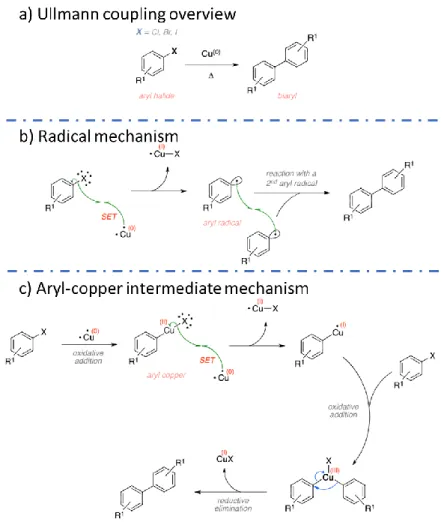
Figure 1-11. Scheme of Ullmann coupling, showing the overall reaction (a) and the two main possible mechanisms, involving either a radical species (b) or an aryl-copper intermediate (c); SET stands for single-electron transfer. Adapted from Ref.95
First discovered in 1901 by the German scientist Fritz Ullmann,96-97 it has been used since then as the most common way to produce biphenyls starting from aryl halides in solution (Figure 1-11a). The reaction is assisted by copper, which needs to be present in the solution in the form of copper powder. The Ullmann coupling is a complex reaction, where different reaction mechanism can be followed depending on the starting precursors, as described by Sambiagio et al.98 In a simplified description, there are two main mechanisms: the first where an aryl radical is produced as an intermediate, and the second where the intermediate is an aryl-copper species. In the radical mechanism (Figure 1-11b), a single-electron transfer takes place between metallic copper and the
aryl halide, to produce the aryl radical and a Cu-X species as a side-product. The aryl radicals then couple to produce the final biphenyl. In the second mechanism, the reaction is started by oxidative addition to a copper atom to form the aryl-copper intermediate. Oxidative addition of a second aryl halide molecule and subsequent reductive elimination produces the final biphenyl. In both cases, dimers of the same aryl halide precursors (homocoupling) or of different precursors (cross-coupling) can be produced. The first instance of on-surface Ullmann reaction was reported by Xi and Bent in 1992. In a series of papers, they described the reaction of iodobenzene precursors on a Cu(111) surface.26, 32, 99 The reaction mechanism was also described, in which a copper atom is inserted into the Cu-I bond to form an organometallic intermediate. The intermediates then react to produce the final biphenyl. Interestingly, they found that two mechanism could be followed, analogous to the ones reported in Figure 1-11 for the solution chemistry case. The reaction pathway depends on the copper atom state, which can be a lattice atom or a surface adatom (Figure 1-12). Xi and Bent were also the first to report a coverage dependence of the on-surface Ullmann coupling, reporting different adsorption behaviors dependent on the surface coverage.26
Figure 1-12 Scheme of on-surface Ullmann coupling: two mechanisms can be observed, depending on whether the involved metallic atoms are from the surface lattice (Mechanism 1) or are
1.5.2 On-surface Ullmann reaction: properties and products
Since 2010, Ullmann coupling has been established as the most common way to produce conjugated polymers on metallic surfaces. The reasons for its popularity are multiple, but the leading ones are the selectivity over the coupling sites and the possibility to perform hierarchical growth offered by the halogen substituents.18, 20 Combined, these two factors allow for precise control of the nanostructures grown, as confirmed by the variety of structures that have been realized, from linear to two-dimensional polymers and even macrocycles. As stated previously, Ullmann coupling is a two-step reaction, in which the first produces aryl radicals that subsequently react, coupling to form a polymer. The radical species are formed by breaking the C-X bonds. By selecting the building block, it is easy to choose the coupling position and therefore a priori decide the final structure obtained.
a. Precise control of radical sites
Figure 1-13 Various porphyrin precursors with 1 (a), 2 (b) or 4 (c) halogens, together with their STM images of a single molecule and the resulting polymeric structure (schematized in the right column); dimers are formed with precursor a, linear chains with b and 2D networks with c. Adapted from Ref.20 with permission from Springer Nature.
The number of reaction sites (i.e. C-X bonds) will control the dimensionality of the nanostructures, as beautifully demonstrated by Grill et al.,18, 20 and reproduced here in Figure 1-13.
In their work they used porphyrin precursors substituted with 1, 2, or 4 halogen atoms to produce dimers, linear chains, and 2D polymers, respectively.
b. Hierarchical growth
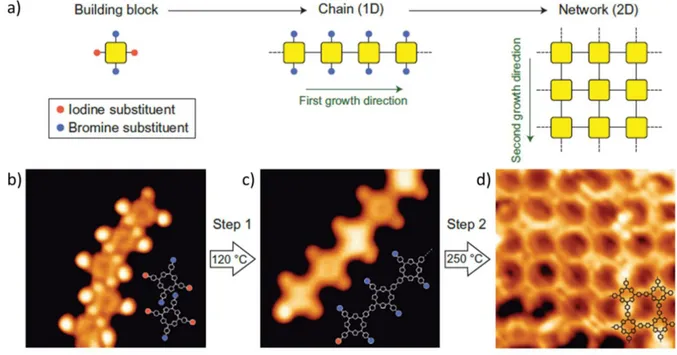
Both steps of the Ullmann reaction can be thermally activated, but the energy required for each step is different and varies depending on the molecule, the surface, and the halogen used. A C-X bond will break at different temperatures depending on the halogen involved. This temperature difference can be exploited to promote hierarchical growth, as first demonstrated by Lafferentz et al.18 in 2012 (Figure 1-14), and subsequently used by multiple researchers with success.101-102 This interesting approach can increase the overall control over the reaction, allowing the initial production of linear chains and then only afterwards converting them into a 2D conjugated structure. It also provides the possibility of studying how the properties change with the dimension of the polymer.101
Figure 1-14 Scheme of hierarchical Ullmann polymerization (a) from an intact molecule to linear chains to 2D networks, together with the respective STM image for each structure in (b), (c), and (d), respectively. Adapted from Ref.18 with permission from Springer Nature.
c. Different possible nanostructures
The properties summarized above can be exploited to realize the desired nanostructures, ranging from simple linear polymers to complex macrocycles or 2D networks, as showed in Figure 1-15.100-101 In some cases, the Ullmann reaction can be coupled with de-hydrogenation reactions to produce a different variety of graphene nanoribbons.103-104
Figure 1-15 STM images of various 1D and 2D structures obtainable with Ullmann coupling, the precursor used and repeating units are reported for each as an inset; a) linear chains, stacked to form 2D domains; b) macrocycles, again stacked to obtain a 2D assembly; c) a 2D conjugated structure with a honeycomb symmetry. a,b) adapted from Ref.100, with permission from
Springer Nature c) adapted from Ref.101 CC BY 4.0
Linear polymeric chains
The easiest kind of polymers that can be obtained via Ullmann coupling on a surface are linear chains, obtained using two halogens per molecule, in a meta or para position. The archetypal precursor for this class of nanostructure is 1,4-dihalobenzene, which was used in the first works to demonstrate the proof-of-concept of on-surface Ullmann coupling. The first studies worth mentioning in this regard were all based on 1,4-dihalobenzenes,19, 30-31, 105-107 and led to a few interesting observations: i. upon absorption on a surface at room temperature, either intact molecules or an OM complex can be formed, ii. whether one or the other is formed is a complex matter, dependent on the halogen type, the surface, and the building-block backbone and iii. to obtain a polymeric structure it is necessary to add energy to the system, either by applying heat, by exposing the system to UV-light or by electron-induced reaction with the STM tip.
Later work focused on the reaction parameters, and discovered that the structures formed also depend on the molecular backbone in addition to the halogen type and the surface.19, 30, 108 All
steps of the transformation, from intact molecules to polymers, were studied by Di Giovannantonio et al. with both STM and fast-XPS in 2012,30 showing that even techniques which average over the surface can be used to follow the reaction. In this work they demonstrated the possibility of following the polymerization step of the on-surface Ullmann coupling, by tracking the evolution of the C 1s molecular peak with temperature and comparing the spectroscopic shift with STM measurements of relative changes in the molecular adlayer. Density functional theory (DFT) calculations were also used to check the validity of the hypotheses made from the STM observations. A number of studies have utilized DFT modeling, to calculate the molecular geometry, to reproduce experimental dI/dV curves by calculating the density of states (DOS), or simply to check if the desired final polymer would be stable and have interesting properties. The widespread application of DFT confirms the importance of this approach, which is complementary to the experimental techniques.16, 109-110 An example of the process and the formed nanostructures can be found in Figure 1-16.
Figure 1-16 Top: scheme of the formation of PPP chains starting from 1,4-dibromobenzene. Bottom: a)
STM image of the obtained OM chains together with b) the respective DFT optimized structure; c) fast-XPS map of the evolution of the C 1s peak during the polymerization reaction, with single line scans between 450 and 475 K as an inset. Adapted from Ref.30 with
Macrocycles
Figure 1-17 a) different ways to obtain the cyclization reaction of linear chains; the vicinity of the C-H groups is highlighted in red. b) Possible geometries of the building block to obtain various closed pore macrocycles upon polymerization. Reproduced from Ref.100
Precursors with two terminal halogens can yield a linear polymer as explained above, but can also undergo a cyclization reaction, via ring-closure. Similar to the case in solution chemistry, precursors with the right structure can form macrocycles via coupling of the reactive ends. An advantage of the surface approach compared with the solution case, is that, being a solvent-free process, insoluble reactants can also be used. However, there are also a few drawbacks, such as the fact that high molecular weight molecules cannot be used, since they would degrade before being sublimated onto the surface (there are ways to cope with this problem however, such as directly dosing liquids in UHV).111 Another drawback of on-surface cyclization is shown in Figure
by bending the C–C 𝜎 bond in a direction perpendicular to the plane of the phenylene units, whereas on a surface, out-of-plane deformation is likely forbidden or limited. The allowed in-plane C-C bending can also lead to disadvantageous strain or, depending on the building block, to steric hindrance (red circle in Figure 1-17a). To avoid these problems, small angles between the phenylene units are required. Depending on the building block, various macrocycles can be formed (Figure 1-17b). However, most of the meta-precursors used can results in both macrocycles and linear chains, depending on the orientation of each added oligomer. For example, in the case of 4,4″-dibromo-meta-terphenyl studied by Fan et al.,100 where the angle between the two C-Br bonds
is 120°, both zig-zag chains and closed cycles are formed. In the same work it was shown that the formation of one structure or the other was dependent on the underlying surface, its temperature during deposition, and the deposition rate. The substrate strongly influences the structure, with three-fold symmetric macrocycles having an higher formation probability on a three-fold symmetric surface, like Cu(111), rather than on a two-fold symmetric one, like Cu(110).112 In addition, low deposition rates favor cyclization over formation of zig-zag chains.100, 113
2D polymers
The holy grail of on-surface polymerization is the formation of long-range ordered 2D conjugated structures, with selected (tunable) properties.34, 114 Various attempts have been made to realize such structures, the first of which was reported by Grill et al. in 2007, where small patches of 2D conjugated polymers were obtained.20 Various researchers tried to improve on this result, varying both the precursors used and the underlying surface, but up to now no polymer structures exhibiting sufficient extent and degree of order to be studied using averaging techniques have been reported, making this the biggest open challenge in the field. Despite falling short, a number of results are worth mentioning that have helped to explain the role of the surface (Figure 1-18),108 show the
DOS of 1D and 2D networks,101, 115 understand how the growth procedure affects the order,102 or
Figure 1-18 a-f) STM images of polyphenylene networks on Cu(111) (a,b), Au(111) (c,d), and Ag(111) (e,f); g-i) Mont Carlo simulations of molecular network growth: coupling probabilities of P = 1, 0.1, and 0.01, for g, h and i respectively, were used for the growth of clusters, which consist of 400 molecules. Below each simulation, the corresponding coordination-number distribution of the molecules in the cluster is given. Adapted from Ref.108 with permission from the American
Graphene nanoribbons
The most advanced and successful application of on-surface Ullmann polymerization so far is the realization of GNRs. This is due to the fact that not only have multiple nanoribbons of various size have been realized, but their extension is sufficient to study them using both STS and angle-resolved photoelectron spectroscopy (ARPES).115 This allowed researchers to obtain information on their properties and even the effect of including heteroatoms in the structures.116-117 Both armchair and zigzag GNRs have been realized and studied, and different procedures were developed to realize one or the other starting from the building block selection.103, 118 Depending on their orientation, these structures possess interesting properties: quantum confinement opens a bandgap in armchair nanoribbons, while zigzag edges are instead expected to host spin-polarized electronic edge states, from which interesting magnetic properties would arise.118 In most cases, Ullmann reaction needs to be coupled with a dehydrogenation step to obtain fully-conjugated GNRs, as shown in Figure 1-19. The hierarchical approach described above was used also for the realization of nanoribbons,119 and procedures have been developed to monitor the synthesis by using solely mass spectroscopy.120
Figure 1-19 a) armchair and zigzag graphene nanoribbon structures, together with an exemplary precursor for armchair GNRs; b) U-shaped dibenzo[a,j]anthracene monomer (1) with halogen functions R1 = Br; c) monomer (1) with an additional dimethyl-biphenyl group in
R2 position, to obtain a zigzag GNR upon polymerization and de-hydrogenation. Reproduced
d. Surface and energies
The outcome of dosing halogenated precursors on a metallic surface can be a priori, but it is a complex function of various parameters, including the choice of building block, the halogen used, the underlying surface (both its composition and orientation), and the substrate temperature.34 While a complete report of all the existing examples in the literature is outside the scope of this thesis, I will give two examples, to allow the reader to understand the complexity of the problem and how important it is to control the parameters and chose the right system.
A good explanation of the surface effect in the dehalogenation process can be found in the 2013 work by Bjork et al.16 In this theoretical paper, they simulated the adsorption of a halobenzene monomer containing either Br or I on three different (111) surfaces of Au, Ag and Cu. They showed that the energy barrier for the de-halogenation strongly depends on both the halogen and the surface, with a lower barrier for iodine, and decreasing from Au to Ag to Cu (Figure 1-20).
Figure 1-20 a) scheme of the energy barrier and reaction energy for a dehalogenation reaction; b) dissociation of bromobenzene on Au(111), depicting top and side views of the initial state (IS), transition state (TS), and final state (FS) of the reaction; c) Energy barrier (left) and reaction energy (right) for the dissociation of bromobenzene and iodobenzene on the (111) facets of Au, Ag, and Cu. Adapted from Ref.16 with permission from the American Chemical Society.
In the same work, they also studied the diffusion of the benzene monomer on the three surfaces, and found that molecular hopping was favored on Au while flipping motion was favored on Ag and Cu. Finally, they addressed the polymerization step, finding an overall lower energy barrier for Cu (Figure 1-21).
Figure 1-21 Energy diagrams for (a) sliding diffusion and (b) flipping diffusion of phenyl on Au(111), Ag(111), and Au(111), where the top and side views of the paths are depicted in the top panel for (a) Ag(111) and (b) Au(111). The flipping diffusion (b) is a two-step process on Cu(111) and Ag(111); c) energy diagram for the coupling reaction of two phenyls into biphenyl on the close-packed facets of Au, Ag, and Cu. Adapted from Ref.16 with permission from the
American Chemical Society.
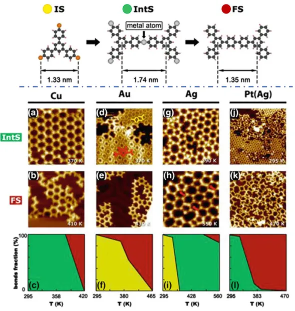
From an experimental point of view, the best example is arguably found in the 2017 work by Dong et al.,121 who studied the reaction of a 1,3,5-4-bromophenyl-benzene on four different surfaces, adding a platinum layer (grown on silver) to the commonly studied copper, gold and silver substrates. As can be seen in Figure 1-22, the resulting structures following RT adsorption are strongly dependent on the substrate, with OM networks observed on Cu and Pt and intact molecules on Au and Ag. Annealing these systems yields polymers on all the surfaces, however on Ag the overlayer passes through an OM phase, whereas on Au a polymer is formed directly upon dehalogenation. The polymerization temperature is also strongly dependent on the surface, and while some C-C coupling can occur at RT on Pt, a temperature of almost 500 K is required on Ag.
Figure 1-22 Top row: reaction scheme from intact precursor (IS) to OM intermediate state (IntS) to polymer (FS) together with key distances optimized by DFT. Middle rows: STM images of the various systems after dosing (a,d,g,j) and after polymerization (b,e,h,k); bottom row: plots of the bonds fraction vs T(K), with color code identifying intact molecules (yellow), OM (green) or polymers (red). Adapted from Ref.121
The most interesting aspect of this work is the fact that no OM bonds are observed on Au. Dong et al.121 assigned the lack of OM networks on Au surfaces to the fact that they are short-lived and thermodynamically unstable. As reported in Figure 1-23, they assign the Au OM phase a higher energy than that required to form the final polymeric phase, concluding therefore that it is only a brief transient of the reaction instead of a stable intermediate as found on other surfaces.