OATAO is an open access repository that collects the work of Toulouse
researchers and makes it freely available over the web where possible
Any correspondence concerning this service should be sent
to the repository administrator:
[email protected]
This is an author’s version published in:
http://oatao.univ-toulouse.fr/24650
To cite this version:
Arico, Cassandra
and Ouendi, Saliha and Taberna, Pierre-Louis
and
Roussel, Pascal and Simon, Patrice
and Lethien, Christophe Fast
Electrochemical Storage Process in Sputtered Nb2O5 Porous Thin Films.
(2019) ACS Nano, 13 (5). 5826-5832. ISSN 1936-0851
Fast Electrochemical Storage Process in
Sputtered Nb
2
O
5
Porous Thin Films
Cassandra Arico,
†,‡,§Saliha Ouendi,
†,§Pierre-Louis Taberna,
‡,§Pascal Roussel,
∥Patrice Simon,
*
,‡,§and Christophe Lethien
*
,†,§†Institut d’Electronique, de Microélectronique et de Nanotechnologie, Université de Lille, CNRS, Centrale Lille, ISEN, Université
de Valenciennes, UMR 8520-IEMN, F-59000 Lille, France
‡Centre Interuniversitaire de Recherche et d’Ingénierie des Matériaux (CIRIMAT), CNRS UMR 5085, Université Paul Sabatier, 118
Route de Narbonne, 31062 Toulouse, France
§Réseau sur le Stockage Electrochimique de l’Energie (RS2E), CNRS FR 3459, 33 Rue Saint Leu, 80039 Amiens Cedex, France ∥Unité de Catalyse et de Chimie du Solide (UCCS), Université de Lille, CNRS, Centrale Lille, ENSCL, Université d’Artois, UMR
8181−UCCS, F-59000 Lille, France
*
S Supporting InformationABSTRACT: The formation of a thinfilm electrode exhibiting high capacity and high rate capabilities is challenging in thefield of miniaturized electrochemical energy storage. Here, we present an elegant strategy to tune the morphology and the properties of sputtered porous Nb2O5 thin films deposited on Si-based substrates via the magnetron sputtering
deposition technique. Kinetic analysis of the redox reactions is studied to qualify the charge storage process, where we observe a non-diffusion-controlled mechanism within the porous niobium pentoxide thin film. To improve the surface capacity of the Nb2O5 porous electrode, the thickness is progressively increased up to 0.94 μm, providing a surface
capacity close to 60μAh·cm−2at 1 mV·s−1. The fabrication of high energy density miniaturized power sources based on the optimized T-Nb2O5films could be achieved for Internet of Things applications requiring high rate capability.
KEYWORDS: Nb2O5, sputtering, thinfilm, lithium intercalation, fast kinetics
P
owering wireless nodes is one of the major challenges within society for the future Internet of Things (IoT), where embedded electronics devices and sensors are connected together to collect and exchange data.1 Indeed, continuous development and further miniaturization of electronic devices such as smartphones, GPS, and tablets greatly stimulate research on the fabrication of small and compact electrochemical energy storage (EES) sources. These small footprint area EES sources have to be efficient in terms of energy, power density, cyclability, and lifespan and should be directly integrated on chips to allow the development of autonomous, sustainable, and connected IoT devices.2,3 To significantly improve the energy density of miniaturized electrochemical capacitors (micro-supercapacitor, MSC) while keeping the power capability of such small devices high,4 aspecific class of microdevices with high energy and power densities able to charge and discharge at high cycling rates has to be developed. To reach this goal, the micro-supercapacitor topology moves from a symmetric configuration (carbon/ carbon, RuO2/RuO2, etc.)taking into account capacitive or
pseudocapacitive electrodesto a hybrid one. Combining the advantage of a capacitive electrode with that of a high-power battery electrode (microbatteries, MB) in an organic electrolyte is an attractive solution to fulfill the requirements. In fact, the energy density of electrochemical capacitors changes with the
voltage squared; as a result, an increase from 1 V (typical cell voltage value when operating in aqueous electrolyte) to 3 V leads to a 9-fold increase in the energy density. This is the reason that one important challenge for supercapacitors and micro-super-capacitors is to use high (pseudo)capacitive materials operating in a large potential window. However, transferring the hybridation concept,5which combines a faradic electrode with a capacitive-like electrode, from the macroscale down to the microscale is challenging. Such a combination allows improving the energy density thanks to the faradic contribution of the battery-type electrode and higher cell voltage. Recently, numerous Li-ion battery (LIB) materials for high-power applications have been investigated where nanosized, highly conductive, and porous-shaped particles are the three key parameters allowing producing high cycling rate and high energy density electrodes. As a matter of fact, materials achieving fast lithium ion intercalation via non-diffusion-controlled reaction kinetics have been prepared, such as MoO3,
6,7
TiO2, 8−12
MoO2,13LiMnO2,14and Nb2O5.15−17
Charge storage in Nb2O5occurs through the intercalation of
lithium ions with concomitant reduction of Nb5+ to Nb4+
expressed as
+ x ++ x −→
Nb O2 5 Li e Li Nb Ox 2 5 (1) where x = 2 corresponds to the maximum theoretical capacity18 of 200 mAh·g−1. To improve the energy density of the carbon-based MSC, the use of Nb2O5as electrode active materials is
promising, as already reported for a classical electrochemical capacitor (EC).19
Nb2O5is an insulating material (σelec≈ 3 × 10⁻⁶S·cm−1)20,21 and exhibits 16 polymorphs, which can be obtained mainly through thermal treatments.15 The formation of each Nb2O5 polymorph depends on the initial precursors, synthesis methods, and heat treatment conditions. The crystalline pseudohexagonal TT-Nb2O5 and orthorhombic T-Nb2O5 phases exhibit Li+
intercalation where a continuous change of potential with state of charge indicates that the lithium intercalation occurs with a single-phase material since their crystalline structure offers suitable transport pathways. B. Dunn et al.16,17,22 have shown that the orthorhombic form of Nb2O5(T-Nb2O5) could
deliver high capacitance at high rate (up to 1000C), confirming the fast lithium ion intercalation/deintercalation processes in such a bulk porous and nanostructured material.16
Integrating Nb2O5material into small IoT devices requires
the miniaturization of the EES source; in that aim, the use of thin film electrodes synthesized by vapor deposition techniques offers attractive opportunities. The fabrication process on silicon chips has to be compatible with the facilities used in the microelectronic industry. Among existing thinfilm deposition technologies to produce binder-free electrodes,24 magnetron sputtering is a powerful tool where the film structure and properties can be tuned according to the deposition parameters (sputtering power, gas pressure, deposition temperature, deposition time).
The present study aims at depositing porous Nb2O5thinfilms
by a dc sputtering technique from a metallic niobium target under an Ar/O2atmosphere. To reach this goal, the pressure is
tuned to study the evolution of the film morphology from compact to porous shape. The as-depositedfilm is then annealed to transform the amorphous Nb2O5(a-Nb2O5) thinfilms into
porous crystallized TT-Nb2O5or T-Nb2O5films exhibiting high capacity at high cycling rate. Once the optimization of the electrochemical properties is reached, the electrode perform-ance has to be maximized: hence, we study the increasing of the film thickness while keeping porous the film morphology to promote the fast lithium interaction process in the crystallized Nb2O5layers.
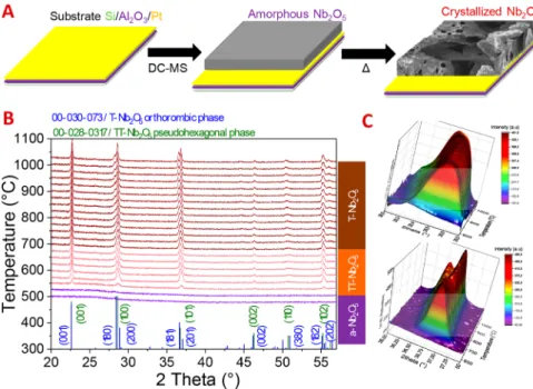
Figure 1. (A) Overview of the electrode design for hybrid microdevices: an amorphous layer is deposited by dc-MS and annealed to form the desired Nb2O5polymorphs (TT-Nb2O5or T-Nb2O5). (B) Evolution of the Nb2O5crystalline phase as a function of the annealing temperature in
high-resolution parallel beam configuration. High-temperature XRD patterns of Nb2O5film deposited on a Si wafer as a function of the
annealing temperature, from 500 up to 1050°C under an air atmosphere. (C) Focus on the diffraction peaks at 2θ = 28.5° and 36.7° corresponding to the (180), (200) and (181) (201) planes of the orthorhombic phase, respectively, and (100), (101) of the hexagonal one.
RESULTS AND DISCUSSION
Optimization of the Annealing Temperature. As mentioned previously, the purpose of this study is thus to prepare sputtered and crystallized Nb2O5porous thinfilms able
to favor the fast Li-ion transport along specific crystallographic pathways (Figure 1A). In this regard, in situ high-temperature X-ray diffraction (HT-XRD) analysis is performed on the as-deposited sample to determine the crystallization temperatures of the Nb2O5polymorphs. Nb2O5 (0.1 μm thick) thin films
deposited at 10−2 mbar on a silicon wafer resulted in the formation of amorphous Nb2O5(a-Nb2O5). XRD patterns are
recorded during an annealing process every 25°C from 50 to 1100 °C in order to determine the annealing temperatures required to reach the formation of the different Nb2O5 polymorphs. Figure 1B shows clearly a three-step process. From room temperature (RT) to 550°C, the niobium pentoxide thinfilm is amorphous (a-Nb2O5). Starting from 575°C, the pseudohexagonal structure TT-Nb2O5is identified (JCPDS
00-028-0317). A splitting of the diffraction peaks (Figure 1C) at 2θ = 28° and 36.5° is observed when the annealing temperature is higher than 650 °C, resulting from the formation of the orthorhombic polymorph T-Nb2O5 (JCPDS 00-030-0873).
From 650 to 700°C, a mix between the TT-Nb2O5and the
T-Nb2O5phases is observed, and at temperature higher that 700 °C the pure T-Nb2O5expected phase is obtained.
Based on these structural conclusions, sputtered Nb2O5thin
films deposited on an Al2O3/Pt current collector are ex situ
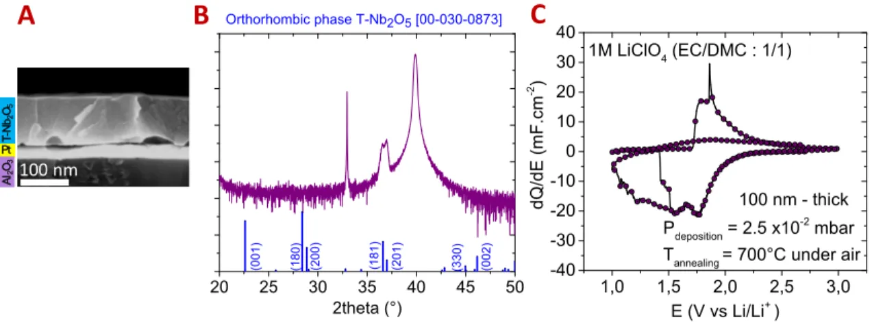
annealed during 2 h under an air atmosphere at 700°C to obtain the expected orthorhombic phase.23Scanning electron micros-copy (SEM) cross section imaging, ex situ X-ray diffraction analyses, and cyclic voltammetry between 1 and 3 V vs Li/Li+are
shown inFigure SI1. Thefilm morphology is found to be highly dense and homogeneous. From the corresponding XRD pattern, a preferential orientation is observed since only the diffraction peak of the (181) plane is visible (Figure SI1-B). From an electrochemical point of view, the observed signature is the expected one. A drastic loss of current during thefirst cycle and a delamination of the thin film from the substrate is observed
(Figure SI1-C). Such delamination is classically observed when
the mechanical stress in thefilm is high and/or when the thin film crystalline network does not offer suitable transport pathways required for Li+ intercalation. In these T-Nb2O5
films (100 nm thick), the stress is known to be high regarding both thefilm density (4 g·cm−3) and the absence of columnar morphology with intra- and intercolumnar porosities.24−26 Moreover, as already pointed out, our thinfilm exhibits a strong preferential orientation along only one direction plane without the [001] crystallographic direction, the most energetically favorable pathways for facile Li.27To avoid these problems, the Nb2O5microstructure has to be porous, stress free, without any cracks or failures, and polycrystalline. Such morphology is similar to the T-Nb2O5nanoparticles synthesized by B. Dunn et
al.22and also enhances the material/electrolyte interface area. To produce such a porous T-Nb2O5 film by a sputtering
technique, a tuning of both the sputtering deposition conditions within the chamber and of the thermal treatment is achieved to fulfill the electrochemical performance requirements.
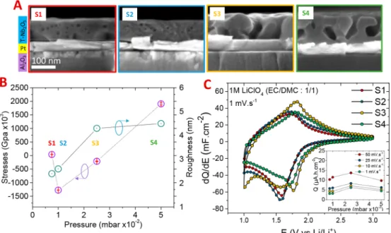
Tuning of the Film Morphology with the Deposition Pressure.Table 1summarizes the deposition parameters of as-deposited Nb2O5 obtained at different pressures, deposition times, and annealing temperatures (samples 1 to 10).Figure 2A shows the SEM cross section of sputtered Nb2O5 thin films
obtained at different pressure conditions and annealed at T = 700°C under N2(samples S1−S4). The melting point of the
Nb2O5compound is Ta= 1793.15 K. For depositions at room temperature, the T
Tm
ratio is lower than 0.2 and the film morphology is found to be in zone T from the Thornton structure zone model (SZM). Indeed, at low pressure (samples S1 and S2) thinfilms exhibit dense granular-like structure, and the surface roughness is very low (∼2 nm). The film densification at low pressure is a consequence of the peening effect and can induce mechanical stress of the thin film. When the pressure is increased (S3 and S4), the morphology moves to a porous granular-like structure with a surface roughness that is still low (∼4.5 nm).
To obtain a stable Nb2O5microstructure without cracks and failures, the stress induced by the Nb2O5films grown on the
silicon wafer has to be investigated. For that purpose, the curvature radius before and after the sputtering deposition has been measured and thefilm stress evaluated using the Stoney formula (Figure 2B). The mechanical stress is minimized at 0.75 × 10⁻²and 2.5× 10⁻²mbar deposition pressure. Nevertheless,
to deposit Nb2O5 thin films without cracks and failures, the
higher pressure (2.5× 10⁻²mbar) offers the best compromise between the roughness and the mechanical stress.
In addition, the kinetics of the lithium ion intercalation process as a function of pressure for T = 700°C is examined.
Figure 2C shows the cyclic voltammetries (CVs) of the four
samples (S1 to S4) at 1 mV·s−1in 1 M LiClO4in ethyl carbonate
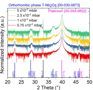
(EC)/dimethyl carbonate (DMC) (1:1) between 1.0 and 3.0 V vs Li/Li+. The four cyclovoltamograms are different due to the type of Nb2O5polymorphs obtained according to the deposition pressure. As a matter of fact, if the pressure is higher than 2.5× 10⁻²mbar, thefilm exhibits a T-Nb2O5orthorhombic structure, as depicted in the diffractograms reported inFigure SI2. Two strong (180) and (200) diffraction peaks occurring at 28.5° are observed, suggesting fast lithium ion transport in such crystallographic pathways. When the pressure is lower than 2.5 × 10⁻²mbar, the TT-Nb
2O5polymorph is clearly highlighted:
only one peak is observed at 28.5°. Therefore, the CVs of samples S3 and S4 are different from the CVs of samples S1 and S2 regarding the number of reduction peaks. A similar observation was reported by B. Dunn et al.16 in 2012. The Nb2O5 film deposited at 2.5 × 10⁻² mbar exhibits higher capacitance and rate capability, demonstrated by the reversible electrochemical signature and the largest current response. The porous microstructure of the sputtered Nb2O5 films at high
pressure is assumed to be responsible for the fast intercalation process of the lithium ion within the bulk material.
Table 1. Deposition and Annealing Conditions of the Samples under Test
pressure (mbar) thickness (nm) time (min) annealing (°C) sample name 7.5× 10⁻³ 100 20 700 S1 1× 10⁻² 100 24 700 S2 2.5× 10⁻² 100 30 700 S3 5× 10⁻² 100 30 700 S4 2.5× 10⁻² 100 30 600 S5 2.5× 10⁻² 100 30 650 S6 2.5× 10⁻² 100 30 750 S7 2.5× 10⁻² 290 90 650 S8 2.5× 10⁻² 580 180 650 S10 2.5× 10⁻² 940 270 650 S11
Then, the influence of annealing treatment was studied. For that purpose, Nb2O5films deposited at 2.5 × 10⁻²mbar have
been annealed during 5 min under a N2atmosphere at 600, 650,
700, and 750°C (rapid thermal annealing process).
The XRD of the S3, S5, S6, and S7 samples is shown inFigure 3A and confirms that all the thin films are polycrystalline (no preferential orientation is observed whatever the annealing temperature is). Here also, the formation of the TT-Nb2O5
polymorph is observed between 550 and 650°C, a mix between the TT-Nb2O5and T-Nb2O5phases is achieved at 650°C, while
the synthesis of the T-Nb2O5occurs beyond 650°C.
Figure 3B shows the CV analysis of the TT-Nb2O5, T-Nb2O5,
and mixed phasefilms at 1 mV·s−1in 1 M LiClO4−EC/DMC
(1:1). Based on the potential difference (inset) between the oxidation/reduction peaks at 1.7 V vs Li/Li+, the fast lithium intercalation/deintercalation process is more reversible in the TT-Nb2O5/T-Nb2O5mixed phase at 650°C compared to the
others.
Based on these optimizations, the deposition pressure and annealing temperature arefixed at 2.5 × 10⁻²mbar and at 650 °C under N2during 5 min, respectively: in that case, a mixed
phase is obtained.
Figure 4A shows cyclic voltammetries for sweep rates between
1 and 100 mV·s−1. For sample S8 (300 nm thick) deposited at 2.5× 10⁻²mbar two broad cathodic peaks at about 1.5 and 1.8 V vs Li/Li+, corresponding to Li-ion intercalation into Nb2O5, are
Figure 2. Study of 100 nm thick Nb2O5thinfilms deposited at different pressures (0.75, 1, 2.5, and 5 × 10⁻²mbar). All the layers are annealed at
700°C under N2during 5 min. (A) SEM cross section analyses as a function of the deposition pressure. (B) Evolution of the intrinsic stress and
the roughness regarding the deposited pressures. (C) Cyclic voltamperometry at 1 mV·s−1between 1 and 3 Vvs Li/Li+of the four studied Nb 2O5
layers. The inset reports the surface capacity as a function of the pressure at different sweep rates. From this study, a deposition pressure at 2.5 × 10⁻²mbar provides the optimal electrochemical performance.
Figure 3. (A) X-ray diffraction analysis of Nb2O5/Pt/Al2O3/Si samples regarding the annealing temperature (P = 2.5 × 10⁻²mbar kept
constant), from 600 up to 750°C (the diffractograms are normalized to the (111) peak of Pt at ∼40°). All the samples are annealed under N2
during 5 min. (B) Cyclic voltammetry at 10 mV·s−1between 1 and 3 Vvs Li/Li+of the four samples, demonstrating the dependent redox activity
with the crystalline polymorphic structure. The inset reports the potential difference between the oxidation and reduction peaks as a function of the annealing temperature at different sweep rates. From this study, an annealing temperature of 650 °C provides the optimal electrochemical performance (more reversible CV and lowerΔE).
observed. During the reverse scan, the set of broad anodic peaks around 1.75 and 1.5 V vs Li/Li+ corresponding to Li-ion
deintercalation from the LixNb2O5 host structure are also observed but a noticeable peak shift and peak separation are
shown when the sweep rate increases. Moreover, the capacity remains reversible.
Constant current charge and discharge cycles of the sample are shown inFigure 4B. A capacity of 160 mAh·g−1is achieved at Figure 4. Electrochemistry analysis of sample S8 (thickness = 290 nm,P = 2.5 × 10⁻²mbar, andT = 650 °C under N2during 5 min). The
electrolyte used is 1 M LiClO4in EC/DMC (1:1). (A) Cyclic voltammetries between 1 and 3 Vvs Li/Li+as a function of sweep rate (1 up to 100
mV·s−1). (B) Galvanostatic cycling of the sample at 1C rate.
Figure 5. Study of the Nb2O5performance as a function of thefilm thickness (P = 2.5 × 10⁻²mbar,T = 650 °C under N2during 5 min). (A) SEM
cross section analysis of the three Nb2O5layers S9, S10, and S11. (B) Cyclic voltammetry of S8, S9, and S10 at 1 mV·s−1between 1 and 3 Vvs Li/
Li+.
Figure 6. (A) Evolution of the surface capacity as a function of thefilm thickness at different sweep rates (1, 5, and 10 mV·s−1) and (B) evolution of the normalized capacity delivered by the Nb2O5electrodes.
1C rate, with a quasi-linear change of the potential with the charge Q.
Improvement of the Electrode Performance for a Miniaturized Power Source. To fulfill the energy require-ment of miniaturized IoT devices, the surface capacity of the electrode has to be improved. An attractive solution to increase the areal capacity of a mixed phase annealed at 650°C under N2 during 5 min and deposited at 2.5× 10⁻²mbar is to increase the thickness of the Nb2O5layers. For this purpose, deposition times are varied (Table 1). From the SEM cross section imaging
(Figure 5A), samples S8, S9, and S10 show a porous
granular-like structure, while the charge of the CVs (Figure 5B) increases with the active mass loading (i.e., the thickness) of the Nb2O5 electrodes. However, as shown inFigure 6A, the areal capacity measured between 3 and 1 V vs Li/Li+reaches 60μAh·cm−2at 1
mV·s−1for a 0.94μm thick Nb2O5film (63.8 μAh·cm−2.μm−1).
The surface capacity does not increase linearly with the film thickness, leading to a small decrease of the volumetric capacity
(Figure 6B) for thicker layers. Nevertheless Figure SI3-A
presents a plot of the cathodic and anodic peak currents observed from the voltammograms ofFigure 4B as a function of sweep rate between 1 and 100 mV·s−1. It is commonly accepted that in a sweep voltammetry experiment the current obeys a power-law28relationship witheq 2:
=
I avb (2)
where I is the current (A), v is the potential sweep rate (mV·s−1), and a and b are specific coefficients related to the diffusion process. The b-coefficient of sample S8 is close to 0.9 for cathodic and anodic currents, indicating that the kinetics is surface-controlled, and thus the charge storage process is fast. For S10, the b-value decreases to 0.7 and 0.75 for anodic and cathodic currents, respectively, showing the emergence of diffusion constraints or an increase of the ohmic contribution at high sweep rate (>25 mV·s−1). This limitation is fundamentally different from battery materials, which are generally characterized by b = 0.5, indicative of a semi-infinite diffusion process.
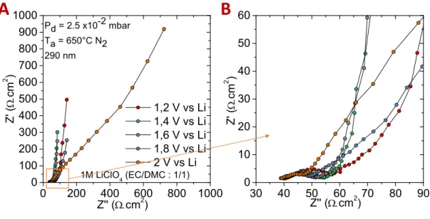
The Nyquist plots (Figure SI3-B) of samples S8, S9, and S10 at 1.6 V vs Li/Li+exhibit an increase of the high-frequency loop
and equivalent series resistance with the film thickness. This behavior can be attributed to the low electronic conductivity of the Nb2O5material together with the thinfilm morphology that
consists of large agglomerated clusters of particles with only intercolumnar porosity (spacing between columns).
CONCLUSION
The present work deals with the synthesis and electrochemical optimization of Nb205electrodes deposited by dc magnetron
sputtering on an Al2O3/Pt-coated silicon wafer. Amorphous Nb2O5thinfilms are sputtered on a Pt-coated silicon wafer and
crystallized into a Nb2O5mixed phase by annealing at 650°C under N2during 5 min. The sputtering deposition pressure is
tuned to promote the formation of porous niobium pentoxide films. Such synthesis conditions favor the formation of a polycrystalline structure exhibiting a porous microstructure required for efficient and fast Li-ion intercalation. The electrochemical analysis demonstrates the absence of diffusion limitations and highlights fast Li-intercalation at 1 mV·s−1. Further studies dealing with the improvement of the Nb2O5 electronic conductivity as well as the evolution of the crystal structure upon cycling using in situ/operando X-ray diffraction analyses on thinfilm electrodes will be achieved in the near
future. Such work clearly validates the important role of the electrode morphology for the fabrication of fast electrochemical energy storage devices for IoT applications.
METHODS
Thin Film Synthesis. Niobium pentoxide (Nb2O5) thinfilms are
deposited by reactive direct current magnetron sputtering (dc-MS) in a CT 200 cluster from Alliance Concept using a metallic niobium target (99.9%, 10 cm diameter, 6 mm thick) under an argon and oxygen atmosphere. The distance between the target and the substrate holder is fixed to 60 mm. Depositions have been carried out on a (100) silicon substrate (diameter = 7.6 cm) coated by layers of Al2O3(thickness =
100 nm) and platinum (thickness = 50 nm). The Pt layer, acting as the current collector, is evaporated using a Plassys MEB 550S apparatus, while the Al2O3layer, deposited by atomic layer deposition (ALD) in a
Picosun R200 reactor, acts as a diffusion barrier to prevent the Pt−Si interdiffusion responsible for the formation of a PtSi alloy, which is likely damaging the current collector.24,25
Before sputtering, the CT 200 cluster is pumped down to 10−6mbar. The power density is kept at 1 W·cm−2 during the sputtering
deposition, while the deposition was achieved at room temperature. Four operating pressures have been studied: 7.5× 10⁻³, 1× 10⁻², 2.5× 10⁻², and 5× 10⁻²mbar. The argon and oxygenflow rates are kept constant at 60 and 10 sccm, respectively. The thickness of the sputtered Nb2O5layers is governed by both the deposition time and the working
pressure. After synthesis, the as-deposited stacked layers (Nb2O5/Pt/
Al2O3/Si) are annealed at 600, 700, or 750°C under N2during 5 min in
an RTA JIPELEC furnace to reach the formation of the TT-, mixed-, or T-Nb2O5 polymorphs, respectively. The deposition time is then
increased to deposit different thickness Nb2O5films.
Morphological, Structural, and Electrochemical Character-izations. The morphology and the thickness of the thin films are determined by SEM) with a Zeiss Ultra electron microscope. The surface roughness is measured by atomic force microscopy (AFM Dimension 3100). To investigate the structure and the crystalline orientation of obtainedfilms, a Rigaku Smartlab multipurpose 6-axis diffractometer (9 kW rotating anode) is used in a high-resolution parallel beam mode (with Soller slits of 5° and a PSD 1D detector DTEX) delivering Cu Kα radiation (lambda = 1.5406 Å). In situ X-ray diffraction measurements are performed in a temperature range from 25 to 1000°C using a DHS 1100 air-filled chamber.
Electrochemical characterizations of the thinfilms were conducted in cells operated in an Ar-filled Fibox. The cells are assembled in a glovebox under an Ar atmosphere, using a Nb2O5thinfilm as working
electrode and pure lithium metal (Sigma-Aldrich) as both reference and counter electrodes. A mixture of 1 M lithium perchlorate salt (LiClO4
Sigma-Aldrich) dissolved in EC and DMC, in 1:1 proportion, is used as the liquid electrolyte. Cyclic voltammetry, electrochemical impedance spectroscopy (EIS), and galvanostatic cycling with potential limitations were performed using a multichannel Biologic VMP3 potentiostat in a two-electrode configuration. EIS measurements are conducted after cycling by applying a 5.0 mVRMSsinusoidal signal amplitude from 100
kHz to 10 mHz at the open-circuit potential at different voltages (from 2 down to 1.1 V vs Li/Li+).
ASSOCIATED CONTENT
*
S Supporting InformationThe Supporting Information is available free of charge on the
ACS Publications websiteat DOI:10.1021/acsnano.9b01457.
Structural, morphological, and electrochemical analyses of T-Nb2O5annealed under an air atmosphere; di ffracto-grams of the Nb2O5films deposited at different pressures;
kinetic analysis of thefilms exhibiting various thicknesses; electrochemical impedance spectroscopy analysis of the film deposited with the optimized pressure and annealed at suitable temperature (PDF)
AUTHOR INFORMATION Corresponding Authors *E-mail:[email protected]. *E-mail:[email protected]. ORCID Pascal Roussel:0000-0001-7243-7293 Patrice Simon:0000-0002-0461-8268 Christophe Lethien:0000-0001-8906-8308 Notes
The authors declare no competingfinancial interest.
ACKNOWLEDGMENTS
This research isfinancially supported by the ANR within the MINOTORES project. The French Renatech network is greatly acknowledged for the microfabrication facilities. The authors also want to thank the French network on electrochemical energy storage (RS2E) and the STORE-EX ANR project for the support. The Ministère de l’Enseignement Supérieur et de la Recherche, Région Hauts de France and FEDER are acknowl-edged for supporting and funding XRD facilities.
REFERENCES
(1) Lethien, C.; Le Bideau, J.; Brousse, T. Challenges and Prospects of 3D Micro-Supercapacitors for Powering the Internet of Things. Energy Environ. Sci. 2019, 12, 96−115.
(2) Huang, P.; Lethien, C.; Pinaud, S.; Brousse, K.; Laloo, R.; Turq, V.; Respaud, M.; Demortiere, A.; Daffos, B.; Taberna, P. L.; Gogotsi, Y.; Simon, P. On-Chip and Freestanding Elastic Carbon Films for Micro-Supercapacitors. Science 2016, 351 (6274), 691−695.
(3) Pech, D.; Brunet, M.; Durou, H.; Huang, P.; Mochalin, V.; Gogotsi, Y.; Taberna, P.-L.; Simon, P. Ultrahigh-Power Micrometre-Sized Supercapacitors Based on Onion-like Carbon. Nat. Nanotechnol. 2010, 5, 651−654.
(4) González, A.; Goikolea, E.; Barrena, J. A.; Mysyk, R. Review on Supercapacitors: Technologies and Materials. Renewable Sustainable Energy Rev. 2016, 58 (C), 1189−1206.
(5) Iwama, E.; Kisu, K.; Naoi, W.; Simon, P.; Naoi, K. Enhanced Hybrid Supercapacitors Utilizing Nanostructured Metal Oxides. In Metal Oxides in Supercapacitors; Elsevier Inc., 2017; pp 247−264.
(6) Kim, H. S.; Cook, J. B.; Lin, H.; Ko, J. S.; Tolbert, S. H.; Ozolins, V.; Dunn, B. Oxygen Vacancies Enhance Pseudocapacitive Charge Storage Properties of MoO3-X. Nat. Mater. 2017, 16, 454−462.
(7) Brezesinski, T.; Wang, J.; Tolbert, S. H.; Dunn, B. Ordered Mesoporous α-MoO3 with Iso-Oriented Nanocrystalline Walls for Thin-Film Pseudocapacitors. Nat. Mater. 2010, 9, 146.
(8) Fehse, M.; Ventosa, E. Is TiO2(B) the Future of Titanium-Based Battery Materials? ChemPlusChem 2015, 80, 785−795.
(9) Zukalová, M.; Kalbáč, M.; Kavan, L.; Exnar, I.; Graetzel, M. Pseudocapacitive Lithium Storage in TiO2(B). Chem. Mater. 2005, 17, 1248−1255.
(10) Wang, J.; Polleux, J.; Lim, J.; Dunn, B. Pseudocapacitive Contributions to Electrochemical Energy Storage in TiO 2 (Anatase) Nanoparticles. J. Phys. Chem. C 2007, 111, 14925−14931.
(11) Wang, J.; Polleux, J.; Brezesinski, T.; Tolbert, S.; Dunn, B. The Pseudocapacitive Behavior of TiO 2 (Anatase) Nanoparticles. ECS Trans 2007, 11, 101−111.
(12) Brezesinski, T.; Wang, J.; Polleux, J.; Dunn, B.; Tolbert, S. H. Templated Nanocrystal-Based Porous TiO2 Films for Next-Generation Electrochemical Capacitors. J. Am. Chem. Soc. 2009, 131, 1802−1809. (13) Kim, H.-S.; Cook, J. B.; Tolbert, S. H.; Dunn, B. The Development of Pseudocapacitive Properties in Nanosized-MoO 2. J. Electrochem. Soc. 2015, 162, A5083−A5090.
(14) Lesel, B. K.; Ko, J. S.; Dunn, B.; Tolbert, S. H. Mesoporous LixMn2O4 Thin Film Cathodes for Lithium-Ion Pseudocapacitors. ACS Nano 2016, 10, 7572−7581.
(15) Kumagai, N. Thermodynamics and Kinetics of Lithium Intercalation into Nb2O5 Electrodes for a 2 V Rechargeable Lithium Battery. J. Electrochem. Soc. 2002, 146, 3203.
(16) Kim, J. W.; Augustyn, V.; Dunn, B. The Effect of Crystallinity on the Rapid Pseudocapacitive Response of Nb2O5. Adv. Energy Mater. 2012, 2, 141−148.
(17) Come, J.; Augustyn, V.; Kim, J. W.; Rozier, P.; Taberna, P.-L.; Gogotsi, P.; Long, J. W.; Dunn, B.; Simon, P. Electrochemical Kinetics of Nanostructured Nb2O5 Electrodes. J. Electrochem. Soc. 2014, 161, A718−A725.
(18) Ohzuku, T.; Sawai, K.; Hirai, T. Electrochemistry of L-Niobium Pentoxide a Lithium/Non-Aqueous Cell. J. Power Sources 1987, 19, 287−299.
(19) Lai, C.-H.; Ashby, D.; Moz, M.; Gogotsi, Y.; Pilon, L.; Dunn, B. Designing Pseudocapacitance for Nb2O5/Carbide-Derived Carbon
Electrodes and Hybrid Devices. Langmuir 2017, 33, 9407−9415. (20) Schultze, J. W.; Lohrengel, M. M. Stability, Reactivity and Breakdown of Passive Fi Lms.Problems of Recent and Future Research. Electrochim. Acta 2000, 45, 2499−2513.
(21) Kats, E.; Zhuiykov, S. Development of Quasi-Two-Dimensional Nb2O5 for Functional Electrodes of Advanced Electrochemical Systems. Int. J. Chem., Mol., Nucl., Mater. Metallurgical Eng. 2013, 353−359.
(22) Augustyn, V.; Come, J.; Lowe, M. A.; Kim, J. W.; Taberna, P.-L.; Tolbert, S. H.; Abruña, H. D.; Simon, P.; Dunn, B. High-Rate Electrochemical Energy Storage through Li+ Intercalation Pseudoca-pacitance. Nat. Mater. 2013, 12, 518−522.
(23) Ouendi, S.; Arico, C.; Blanchard, F.; Codron, J.-L.; Wallart, X.; Taberna, P. L.; Roussel, P.; Clavier, L.; Simon, P.; Lethien, C. Synthesis of T-Nb2O5 Thin-Films Deposited by Atomic Layer Deposition for Miniaturized Electrochemical Energy Storage Devices. Energy Storage Mater. 2019, 16, 581−588.
(24) Hallot, M.; Lethien, C.; Brousse, T.; Létiche, M.; Roussel, P.; Huvé, M. Tuning the Cation Ordering with the Deposition Pressure in Sputtered LiMn 1.5 Ni 0.5 O 4 Thin Film Deposited on Functional Current Collectors for Li-Ion Microbattery Applications. Chem. Mater. 2017, 29, 6044−6057.
(25) Hallot, M.; Demortière, A.; Roussel, P.; Lethien, C. Sputtered LiMn1.5Ni0.5O4 Thin Films for Li-Ion Micro-Batteries with High Energy and Rate Capabilities. Energy Storage Mater. 2018, 15, 396−406. (26) Robert, K.; Douard, C.; Demortière, A.; Blanchard, F.; Roussel, P.; Brousse, T.; Lethien, C. On Chip Interdigitated Micro-Super-capacitors Based on Sputtered Bifunctional Vanadium Nitride Thin Films with Finely Tuned Inter- and Intracolumnar Porosities. Adv. Mater. Technol. 2018, 3, 1800036.
(27) Kumagai, N.; Tateshita, Y.; Takatsuka, Y.; Baba, M.; Ikeda, T.; Tanno, K. Intercalation of Lithium in r.f.-Sputtered Niobium Oxide Film as Electrode Material for Lithium-Ion Batteries. J. Power Sources 1995, 54, 175−179.
(28) Lindström, H.; Södergren, S.; Solbrand, A.; Rensmo, H.; Hjelm, J.; Hagfeldt, A.; Lindquist, S.-E. Li+ Ion Insertion in TiO2 (Anatase). 2. Voltammetry on Nanoporous Films. J. Phys. Chem. B 1997, 101, 7717− 7722.
1
Fast Electrochemical Storage Process In Sputtered Nb
2
O
5
Porous Thin Films
Supporting Information
1,0 1,5 2,0 2,5 3,0 -40 -30 -20 -10 0 10 20 30 40 100 nm - thick 1M LiClO4 (EC/DMC : 1/1) Pdeposition = 2.5 x10⁻² mbar Tannealing = 700°C under airdQ /d E ( m F .c m -2 ) E (V vs Li/Li+ ) 100 nm Pt A l2 O3 T-N b2 O5 20 25 30 35 40 45 50 2theta (°) (0 02 ) (2 00 ) (1 80 ) (3 30) (201 ) (1 81 ) (001 ) Orthorhombic phase T-Nb2O5 [00-030-0873]
A
B
C
Figure SI1: A. SEM cross section analysis of the Nb
2O
5thin film deposited at 2.5 x10
-2mbar and annealed under air at 700°C during 2h. B. X-ray diffraction analysis after air
annealing showing a preferential orientation at 36.7°. C. First two cycles of cyclic
2
voltammetry at 1 mV.s
-1showing the current leakage, consequently the thin film
delamination.
20 25 30 35 40 45 50 Platinium [00-004-0802] N or m al iz ed in te ns ity ( a. u. ) (1 1 1 ) (3 30 )Orthorhombic phase T-Nb2O5 [00-030-0873]
2 Theta (°) 5 x10⁻² mbar 2.5 x10⁻² mbar 1 x10⁻² mbar 0.75 x10⁻² mbar (2 0 0 ) (0 02 ) (2 01) (1 81 ) (2 00 ) (1 80) (001 ) S i