O
pen
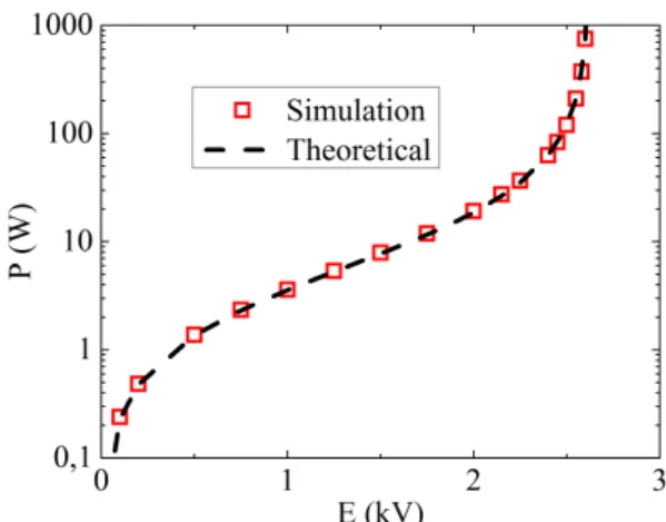
A
rchive
T
OULOUSE
A
rchive
O
uverte (
OATAO
)
OATAO is an open access repository that collects the work of Toulouse researchers and makes it freely available over the web where possible.
This is an author-deposited version published in : http://oatao.univ-toulouse.fr/ Eprints ID : 17741
To link to this article : DOI:10.1088/1742-6596/825/1/012004
URL :
http://dx.doi.org/10.1088/1742-6596/825/1/012004
To cite this version : Diop, Mame Andallah and Belinger, Antoine and
Piquet, Hubert DBD tranformerless power supplies: impact of the parasitic capacitances on the power transfer. (2017) Journal of Physics: Conference Series (JPCS), vol. 825. pp. 012004. ISSN 1742-6588
Any correspondence concerning this service should be sent to the repository administrator: [email protected]
DBD tranformerless power supplies: impact of the parasitic
capacitances on the power transfer.
M A Diop1, A Belinger1, H Piquet1
1LAPLACE, Université de Toulouse, CNRS, INPT, UPS, France
Abstract. A new transformerless power supply for DBD application is presented here. The
power supply is built with 10kV SiC MOSFET. This high voltage switches allow holding the high voltage required by the DBD. An analytical study of the converter’s operation is presented to deduce the power transmitted to the DBD. A comparison between the experimental and theoretical electrical waveforms is shown. The experimental waveforms are particularly affected by all the parasitic capacitances. When all the switches are in OFF state, oscillations cause over-voltages across the switches. An analysis of the effect of each capacitance is presented and demonstrates that the parasitic capacitances of the switches and of the inductance play a key role in the actual power transfer.
1. Introduction
Dielectric Barrier Discharges (DBD) is a device where it is easy to establish cold plasma at atmospheric pressure [1]. For this reason, DBDs have a lot of applications: ozone generator [2], excimer lamp [3], surface treatment [4], flow control actuators [5]… In Dielectric Barrier Discharge (DBD) setups, at least one dielectric is placed between the two metal electrodes that supply the gas. The dielectric enables to limit the local current of the discharge, even despite a large pd product (p is the pressure and d the gas gap). From an electrical point of view, DBD are capacitive loads. So they must be supplied by an alternative current source. Furthermore, to ignite the discharge at atmospheric pressure, the applied voltage usually reaches several kilovolts. This high alternating voltage is traditionally obtained via amplification, using a step-up transformer. A DBD is a capacitive charge: for a sinusoidal source the current and the voltage are delayed by 90 degree; this implies a high consumption of reactive power and an over-sizing of the transformer in order to sustain the maximum voltage and rms current required by the DBD. Therefore the transformer is often very heavy and cumbersome. For example for a 100W DBD, the volume of the transformer is often up to 1 liter. In classical electronic application this volume is used for a 1kW system. Moreover, the parasitic elements of the transformer (leakage inductance, inter-turn and inter-winding parasitic capacitance), specific to the physical structure of this device, limit the power transfer. For example, parasitic capacitances of the transformer have the same order of magnitude as those of the DBD. They are parallel to the DBD, so they divert a significant part of the current [6]. This also slows down the voltage rise and delays the ignition of the discharge.
Improving these issues and the over-sizing incited us to investigate power supplies for DBD without transformer. A voltage inverter is directly connected to the DBD. It involves the use of
high-voltage switches. Because high-high-voltage switches are available only for a few years, only theoretical developments have been proposed to date [7]. Using 10kV SiC DMOSFET, an innovative transformerless pulsed-current source topology is proposed here and is detailed. The theoretical calculation of the transferred power is presented in a first part. Afterwards we show that the parasitic capacitances affect the operating conditions. We analyze the impact of each parasitic capacitance on the quality of the power transfer. Each capacitance is studied separately in order to understand its impact.
2. Experimental setup and power supplies operating
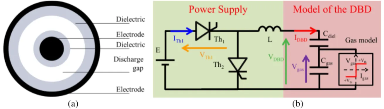
In a power-supply design approach, the modelling of the DBD is developed below [8]. The DBD used for the experiments is an excimer UV lamp with a cylindrical configuration, with two dielectric barriers and two coaxial tubes of quartz containing a volume of a Xe-Cl gas mixture at 120mBar (Figure 1.a). Metal electrodes are placed on their outer walls. Concerning the geometry of the lamp, the length of the lamp is 115mm and the gap is 20mm.
As long as the discharge is in OFF state, the DBD is modelled by two capacitors in series: Cdiel and Cgas. The latters correspond respectively to the dielectrics and to the gas capacitance. The geometrical characteristics allow to estimate these capacitances: Cgas=28pF and Cdiel=85pF. When the discharge is in ON state, we consider that the gas voltage remains constant, ±Vth (the sign depends on the direction of the current). This assumption is accurate when the discharge is a Townsend or glow mode; it does not take local phenomena into account, but concerns a macroscopic point of view. For a power-supply design approach, it is sufficient to take into account the non-linearity of the plasma [9]. As shown in Figure 1.b the discharge is electrically modelled by a (Vgas, Igas) dipole taking into consideration the non-linearity explained above; this dipole is parallel to the gas capacitance Cgas. The breakdown voltage was measured at Vth= 1310kV. In the whole paper, we develop the analysis with this lamp; however the general conclusions are valid for any DBD device.
(a) (b)
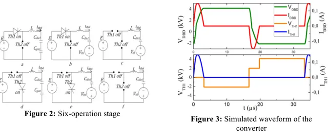
Figure 1: (a) Diagram of the DBD lamp. (b) Diagram of the power supply and electrical model of the DBD
Due to the capacitive nature of the DBD and the electrical characteristic of the discharge, the DBD must be supplied by a current source generator [10]. In steady state, the DBD current must have a null average value. Therefore, in the topology presented in Figure 1.b, an inductor is placed in series with the DBD; a constant source voltage E supplies this circuit and the direction of the current depends on the state of the switches.
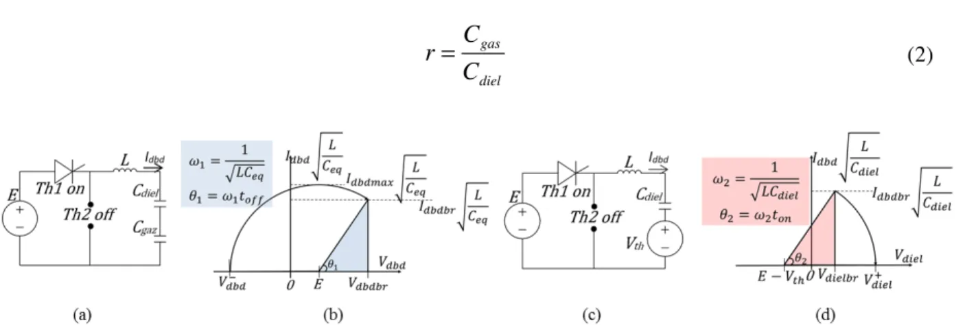
On the basis of the electrical constraints (voltage and current waveforms) described in the following lines, it can be shown that the characteristics of both semiconductors are those of a thyristor. At the range of the target frequencies (tens of kHz) there is no thyristor on the market, so this function is synthesized by combining in series a MOSFET and a diode [11]. The operation of the converter is presented in Figure 2. In the first sequence (Figure 2.a), the thyristor Th1 is closed, thus the high voltage source supplies the resonant L/Ceq circuit (Ceq correspond to the capacitances Cdiel in series
with Cgas). The DBD current IDBD and the DBD voltage VDBD are controlled by the L/Ceq circuit until the
gas breakdown. As soon as the discharge is ignited, the gas voltage Vgas remains constant at +Vth, and
IDBD and VDBD are then governed by the resonant loop L/Cdiel (Figure 2.b) until IDBD drops to zero, and the opening of Th1. The extinction of the discharge results in the opening of the thyristor Th1. Afterwards, there is no evolution of IDBD and VDBD until the closing of Th2. When Th2 is turned ON, the DBD and the inductor are short-circuited. The charges accumulated on the dielectric are then used to re-ignite the discharge. The evolution of the electrical waveforms of the DBD is governed by the same resonant circuits: L/Ceq as long as the discharge is OFF (Figure 2.d), and L/Cdiel when it is ON (Figure 2.e). The ideal waveforms of Vgas and Idbd are symmetrical with respect to those obtained in the first half period. An important part of the charges, stored on the dielectrics during (a)-(b), is dissipated in the discharge and the semi-conductors during phase (d)-(e). Therefore in Figure 3 VDBD voltage may not be symmetrical.
Figure 2: Six-operation stage
Figure 3: Simulated waveform of the converter
It is important to note that the switch voltage reaches the DBD voltage. In the case of a synthesized thyristor, the MOSFET holds the positive voltage and the diode the negative voltage.
3. Theoretical power dissipated in the discharge
The operation of this converter is studied using the state plan analysis [12] from the model shown in Figure 3. This graphical analysis allows building the trajectories of the current-voltage point of a resonant circuit. Assuming that the steady state is reached, on positive half cycle the operating point describes during a first stage (Figure 4.a) a part of a circle centred on Vdbd=E and Idbd=0, until the gas breakdown (Figure 4.b); at this time, Vgas=Vth. and the Vdbd voltage takes the Vdbdbr value.
Once the discharge is ignited, the gas capacitance is charged to Vgas=Vth. During a second stage (Figure 4.c), the part of the circle is centred on Vdiel=E-Vth and Idbd=Idbdbr (Figure 4.d), until Vdbd= V+dbd (Vdbd voltage when current cancels). In this study, only the positive half-wave is treated. A complete study of the two half periods (work not presented here) has allowed verifying that the current Idbd is symmetrical.
The maximum DBD voltages of the negative and of the positive halves are respectively referred to V -dbd and V+dbd. One can notice that V-dbd=E- V+dbd.
Using Figure 4.b and Figure 4.d we can deduce:
(1) With:
V
dbd +=
4
⋅V
th 21
+ r
(
)
− E
24
⋅V
th− 2 ⋅ E
(2)
Figure 4: Phase plan analysis. (a): diagram before breakdown. (b): phase plan before breakdown. (c): diagram during the discharge. (d): phase plan during the discharge
The energy En dissipated in the discharge during the first half period is:
E
n= V
th⋅
i
dbd(t)
⋅dt
tbreakdown toff
∫
= V
th⋅C
diel⋅ V
(
diel( )
t
off−V
diel(
t
breakdown)
)
= V
th⋅C
diel⋅ V
diel+
−V
dielbr(
)
(3)with tbreakdown the time og the gas ignition and toff the end of the discharge. To calculate the energy, we need the expression of V+
diel and Vdielbr. When the discharge is ignited (between tbreakdown and toff) the dielectric voltage is:
V
diel( )
t
= V
dbd( )
t
−V
th (4) so we deduce V+ diel:V
diel += V
diel( )
t
off= V
dbd +−V
th (5)To calculate Vdielbr, we need the expression of Vdbdbr obtained from the integration of Vdbd between the time of Th1 switching ON (t=0) and the time of the gas ignition (t=tbreakdown):
Vdbdbr−Vdbd − = dVdbd = 1 Ceq idbd⋅dt = Cgas Ceq ⋅ dVgas t=0 tbreakdown
∫
t=0 tbreakdown∫
t=0 tbreakdown∫
= 2 r +1(
)
⋅Vth (6)So combining the equation (4) and equation (6) : Vdielbr= Vdbd
− + V
th⋅ 2 ⋅r +1
(
)
(7)From equations (3), (5) and (7), the energy dissipated in the first half period is:
E
n= 2 ⋅C
gas⋅V
th2⋅
E
2
⋅V
th− E
(8)The energy dissipated in the first half period is equal to the energy dissipated in the second half period so the power P dissipated in the discharge is:
P
= 4 ⋅C
gas⋅ f ⋅V
th2E
2
⋅V
th− E
(9)The evolution of the power dissipated in the discharge P versus the power supply voltage E is plotted in Figure 5. The circuit presented in Figure 1.b is simulated using PLECS. The simulation confirms
r
=
C
gasC
dielthe theoretical equation presented in equation (7). It should be noticed that the inductance has no influence on the power. Its value only adjusts the duration of the discharge and the magnitude of the current.
Figure 5: Power transmitted to the discharge versus the power supplies voltage for a frequency of 30 kHz
As long as E is lower than 2000V, the power delivered to the DBD increases slowly. When E tends to 2Vth, the power tends toward the infinity. In this case at the end of each half cycle the dielectric voltage (or the charge stored on the dielectric) are increased. So, the breakdown appears earlier during the period and the maximum current Idbd of the next discharge increased. Steady state cannot be found. As shown in equation (9), it is possible to adjust the power P by the frequency and by E. However, it is important to limit E to a value below lower than 2Vth.
4. Experimental validation
A prototype of this power converter has been realized using high voltage switches: SiC power DMOSFET from CREE with a 10kV maximum drain to source voltage are used. The series connected diodes C4D02120A, holding up to 1700V from CREE are used. Throughout the whole paper (for experiment or for simulation), the inductance value is 17mH. At 30kHz and with the lamp used here, the duration of the pulse is always lower than the half period. Therefore, the switch operates really as a thyristor. The volume and the weight of the power supply are very weak compared to a power supply with a transformer.
The voltages are measured using high-voltage differential probes, TESTEC TT-SI 010 A, and the current is measured using a 4100 Pearson probe. Electrical waveforms are recorded using a LECROY Wavesurfer 24XS oscilloscope. The constant voltage source E is an adjustable power supply (SFRDO-F-2000, Technix brand).
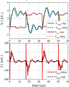
The electrical waveforms (Vdbd, Idbd and Vth1), measured at 30kHz and E=3 kV, are presented in Figure 6. The time evolution of Vth2 is the same as for Vth1, delayed by a half period. When the discharge turns ON the waveforms are very close to those presented above. According to the previous theoretical analysis, it has been unexpected to observe some oscillations in all the waveforms when the discharge and the switches turn OFF. This is because the diagram of the power supply presented in Figure 1.b is simplistic and does not take into account the parasitic elements. As can be seen, the oscillations cause over-voltage across the semiconductors. This can be a serious issue for transformerless power supply, because high voltages switches must sustain this over-voltage and are currently limited to 10kV. In Figure 7 we present a simulation model of the power supply taking into account all the parasitic capacitances. The value of the MOSFET capacitance Cossi and of the diode capacitance Cdi are taken from the datasheet and arranged in a table indexed by semiconductor voltage. The parasitic capacitance of the inductance Cpara_L is measured by an impedance bridge and is equal to 5pF. The
probe capacitance Cprobe is also measured using two current probes (one upstream and one downstream the voltage probe). Finally a parasitic capacitance Cpara is inserted between the probe and the DBD. This last parasitic capacitance takes into account the high voltage connection to the DBD (wire, high voltage terminals …). Cpara is measured when the discharge is OFF by a basic current voltage method and its value is 15pF.
Figure 6: Electrical waveform: comparison between experimental measurement and
simulation of the diagram of Figure 7.
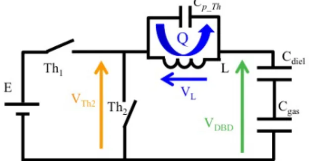
Figure 7: diagram of the power supply tacking into account al the parasitic capacitance.
The power supply with all the parasitic capacitance presented in Figure 7 is simulated with PLECS. As presented in Figure 6, this simulation accurately fits the measured waveforms: same amplitude, same oscillation frequency. The oscillations observed after the extinction of the discharge are therefore due to the parasitic capacitance presented in Figure 7. If all these parasitic capacitances are not taken into account, the frequency and the amplitude of the oscillations are not accurate. Nevertheless, in order to simplify the analysis, we consider in the following sections separately the role of each parasitic capacitance.
5. Influence of the parasitic capacitance of the switches
In this part we use the basic thyristor model developed by PLECS. For each thyristor, Th1 and Th2, only a constant capacitance Cp_Th takes into account the parasitic effects as seen in Figure 8. In Figure 10.b, the simulated waveforms of VDBD, Vdiel, VTh2 and, iTh1 are presented for the first half period (when Th2 is in OFF state) and for a frequency of 30kHz. When Th1 is turned ON, the waveform does not change with or without parasitic capacitances. During this phase, the parasitic capacitance of Th1 is short-circuited and the one of Th2 is charged to E: no charges are transferred between these parasitic capacitances and other elements of the circuit. As long as Th1 is ON, its parasitic capacitance plays no role. When the current of Th1 drops to zero, the discharge extinguishes and Th1 blocks spontaneously. So all switches are OFF and electric charges move between the DBD and the switches parasitic capacitances. Indeed, voltage is not imposed on Cp_Th. The charge transfer leads to oscillations that are visible in all the electrical waveform. Therefore the parasitic capacitances of the switches are the only
responsible of these oscillations. It is not shown here, but it is easy to understand that the same phenomenon appears on the second half period (Th1 remains OFF).
Figure 8: Power supply with only the parasitic capacitances of the switches.
Figure 9: Power transferred to the discharge. Full line: with a parasitic capacitance of 20 pF.
Dashed line: Without parasitic capacitances (equation (9))
In Figure 9, we present the evolution of the power versus the constant voltage E for a parasitic capacitance Cp_Th of 20pF (red curve). This value corresponds to the order of magnitude of a high voltage switch.
Figure 10: Simulated electrical waveform of the power supply with a parasitic capacitance. First half period when Th1 turned OFF and Th2 turned ON. Switching time are indicated (a): Cp_Th=7.8pF.
Bracket *: local maxima of Vdiel. Bracket m: local minima of Vdiel. (b): Cp_Th=13pF.
As can be seen in Figure 9, parasitic capacitances of the switches clearly affect the power transferred to the discharge. With switch parasitic capacitances, the power is lower than without switch parasitic capacitances. Moreover with switches parasitic capacitance, the powers do not present a hyperbolic trend when E is close to 2Vth. The power supply can operate in a wider range of voltage E. Indeed, as soon as all the thyristors are open, the parasitic capacitances of the switches discharge the dielectrics of the DBD. In any case, compared to the theoretical case, fewer charges are stored on the dielectrics when a thyristor is closed. If fewer charges are available to ignite the next discharge, the energy dissipated will be lower. This phenomenon explains why the power dissipated in the discharge with Cp_Th is lower than the power dissipated in the discharge without parasitic capacitances.
Figure 11 presents the evolution of the power transferred to the discharge versus Cp_Th for a frequency of 30kHz and E=3kV. Overall, the power tends to decrease with Cp_Th but there are local maxima where the power strongly increases.
To understand these power peaks we have to look carefully at the temporal evolution of VTh2 and Vdiel presented in Figure 10.a and Figure 10.b. The Figure 10.a corresponds to a power peak, and Figure 10.b corresponds to a power deep. As can be seen, the numbers of local minima and maxima on Figure 10.a and Figure 10.b are different. The parasitic capacitance changes the oscillations frequency and the number of oscillating periods during the OFF time of the discharge (when Th1 and Th2 are in OFF state). In some cases, Th2 is closed when Vdiel is maximal and there is a power peak (Figure 10.a), in other cases Th2 is closed when Vdiel is minimal and there is a power deep (Figure 10.b). Therefore we observe a power deep when fewer charges are stored on the dielectric, and at the opposite we observe a power peak when more charges are present on the dielectric. This further regard confirms that the power dissipated in the discharge strongly depends on the charges stored on the dielectric before the closing of the switches.
Figure 11: Evolution of the transferred power versus the switch parasitic capacitance for E=3kV and f=30kHz.
The parasitic capacitances of the switches modify the power transferred in the discharge. In some case the values of the parasitic capacitances amplify the power transferred in the discharge. Improving the power transfer requires to take these parasitic capacitances from the very early stage of the design. Anyway, it is impossible and illusory to imagine adjusting perfectly the value of the parasitic capacitances.
6. Influence of the voltage probe capacitance
The probe capacitance Cprobe or the parasitic capacitance Cpara (which consists of the connection and the wire) do not substantially change the situation explained above; their impacts is mainly a change of the resonant frequency that defines the duration of the current pulses.
If the switches parasitic capacitances are not considered, there are no additional oscillations (with respect to the theoretical waveforms of Figure 3) when all the switches are in OFF state; the P(E) plot (power P versus E voltage) keeps the hyperbolic shape presented in Figure 5 and shown again on Figure 9.
With switches parasitic capacitances, the oscillations always exist when both switches are OFF. Cprobe affects the oscillation frequency and the Cpara or Cprobe capacitances shift lightly the curve presented in Figure 11, but do not change fundamentally the operation of the power supply.
Moreover, if a voltage probe is connected to switch terminals, its parasitic capacitance will play the same role as the parasitic capacitance of the switch.
7. Influence of the parasitic capacitance of the inductance
Depending on the presence of the switches capacitances, the parasitic capacitance of the inductance affect markedly the operating of the power supply.
7.1. Without switches parasitic capacitances
We use PLECS to simulate the power supply presented in Figure 1.b but we add a capacitance of Cpara_L=5pF in parallel with the inductance. The time evolution of VTh2, VDBD, Vdiel and Idbd is presented in Figure 13. The time evolution of Vth1 is the same that the time evolution of Vth2 delayed by a half period.
Figure 12: Charges transfer when all the switches and the discharge are OFF
When all the switches are OFF (Figure 12), the oscillating circuit consists on L in parallel with only Cpara_L. The moving charges Q are presented in Figure 12. Because all the switches are in OFF state, no current flows through the DBD and the DBD voltage remains constant. The switches voltage is equal to the DBD voltage plus the voltage of oscillating circuit L/Cpara_L (Figure 13).
Figure 13: Electrical waveform with parasitic capacitance of the inductance. E=2kV, f=30
kHz.
Figure 14:Evolution of the power with only an inductance parasitic capacitance Cpara_L=5pF.
f=30kHz
When one switch is turned ON we observe a current spike on IDBD. This is due to a sudden change of the voltage applied on the inductance parasitic capacitance. According to the current ratings of the semiconductor, these spikes could damage the switches. Moreover, when the switching appears, a strong and swift voltage step is directly applied on the series circuit consisting in the DBD and the inductance. Without Cpara_L the inductance L sustains the totality of the voltage step. With Cpara_L, this voltage step is applied to the 3 capacities in series: Cpara_L, Cgas, Cdiel. As we can see in Figure 13, it causes a slight drop of VDBD and Vdiel as soon as Th1 or Th2 turns ON. As explain above, a drop of the dielectric voltage causes a limitation of the power. As shown in Figure 14, with only the parasitic capacitance of the inductance, the power plot P(E) are not an hyperbolic trend; Cpara_L limits the power transferred to the discharge.
7.2. With switches parasitic capacitances
The operating is nearly the same as the one described in the part 5 (with only the parasitic capacitances of the switches). However, the current spike is now present as explained above in 7.1. Due to its low value, Cpara_L affect scarcely the operation of the power supply on the power transfer.
8. Conclusion
Aimed at limiting the negative effects of the high voltage step up transformer, an innovative transformerless topology for DBD has been proposed.
This specific resonant inverter operates as an instantaneous current source and supplies the DBD with positive and negative current pulses. The properties of these pulses (magnitude, duration, frequency f, direction) are fully adjustable using the design (values of the circuit's components) and operating degrees of freedom (firing orders, magnitude E of the DC source).
10kV high voltage SiC MOSFETs and diodes are used to synthesize the thyristor-like characteristic of the power switches. These devices, as well as the resonant inductor, introduce parasitic capacitances. The most important points concerning these parasitic capacitances are:
• An increase of the voltage stresses on the semiconductor SiC devices;
• A modification of the output power due to the drop of the charges stored on the dielectrics of the DBD. This charges are diverted to the parasitic capacitances of the switches when the latter are OFF;
• A current spikes in the switches at turn ON, due to the sudden voltage step of the inductance's parasitic capacitance.
As a matter of fact, all these side effects substantially modify the operating conditions of the semiconductors and need to be early accounted at design step. A special care at implementation stage needs to be taken in order to reduce the parasitic capacitances as much as possible.
References
[1] Kogelschatz U 2003 Plasma Chem. and Plasma Proc. 23 26
[2] Williamson J, Trump D D, Bletzinger P and Ganguly B N 2006 J. Phys. D: Appl. Phys. 39 4400 [3] Lomaev M I, Skakun V S, Sosnin E A, Tarasenko V F, Shitts D V and M V Erofeev 2003 Phys.
Usp. 46 193
[4] Massines F, Sarra-Bournet C, Fanelli F, Naudé N and Gherardi N 2012 Plasma Process. and Poly 9 1041
[5] Corke C T, Post M L and Orlov D M 2008 Exp. Fluids 46 1
[6] Bonnin X, Piquet H, Diez R, and Florez D 2013 15th European Conference on Power Electronics and Applications (Lille) pp. 1-9
[7] El-Deib A, Dawson F and Zissis G 2011 IEEE Energy Conversion Congress and Exposition (Phoenix) pp 1124-1131
[8] Díez R, Salanne J P, Piquet H, Bhosle S, and Zissis G 2007 Eur. Phys. J. - Appl. Phys. 37 307 [9] Bonnin X, Piquet H, Naudé N, Bouzidi M C, Gherardi N and Blaquière J M 2013 Eur. Phys. J.
Appl. Phys. 64 10901
[10] Piquet H, Bhosle S, Diez R, and Erofeev M V 2010 IEEE Trans. Plasma Sci. 38 2531 [11] Cousineau M, Diez R, Piquet H, Durrieu O 2012 IEEE Trans. Ind. Electron. 59 1920 [12] Chéron Y 1992 Soft Commutation (Springer Science & Business Media)