HAL Id: hal-01570282
https://hal.archives-ouvertes.fr/hal-01570282
Preprint submitted on 28 Jul 2017
HAL is a multi-disciplinary open access archive for the deposit and dissemination of sci-entific research documents, whether they are pub-lished or not. The documents may come from teaching and research institutions in France or abroad, or from public or private research centers.
L’archive ouverte pluridisciplinaire HAL, est destinée au dépôt et à la diffusion de documents scientifiques de niveau recherche, publiés ou non, émanant des établissements d’enseignement et de recherche français ou étrangers, des laboratoires publics ou privés.
Statistical Methods Applied to CMOS Reliability
Analysis -A Survey
Hao Cai, Jean-François Naviner, Hervé Petit
To cite this version:
Hao Cai, Jean-François Naviner, Hervé Petit. Statistical Methods Applied to CMOS Reliability Anal-ysis -A Survey. 2017. �hal-01570282�
Statistical Methods Applied to CMOS Reliability Analysis
- A Survey
Hao Cai, Jean-Franc¸ois Naviner, Herv´e Petit
Institut Mines-T´el´ecom, T´el´ecom-ParisTech, LTCI-CNRS-UMR 5141
1
Introduction
The design of integrated circuits (ICs) and systems in sub-90nm CMOS technology is very challeng-ing [1]. The scalchalleng-ing down of technology not only caused an unbalanced relationship between
sup-ply voltage and transistor threshold voltage (Vth), but also induced ageing effects and variability
prob-lems [2, 3]. In semiconductor manufacturing, systematic and random variations exist during different fabrication steps. Moreover, once ICs are fully functional, both ageing and variability degrade ICs per-formance and lead to uncertainty perper-formance distribution. In this paper, we analysis process variations based on BSIM4 transistor model.
1.1 Traditional methods
From the perspective of designers, in order to know the variability and yield information, One traditional method is to setup guardband with worst-case corner-based analysis. In SPICE-like simulator, NMOS and PMOS type transistors are defined with letter acronyms (F: fast, S: slow and T: typical). For example,
NMOS and PMOS transistors with low oxide thickness (Tox), threshold voltage (Vth) is represented with
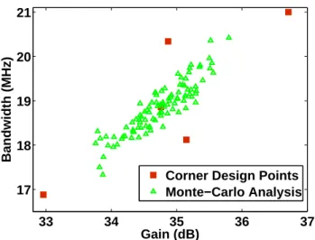
’FF’ type (fast NMOS, fast PMOS). The other widely applied method is Monte-carlo analysis (see Figure 1). The performance distribution can be evaluated through a large amount of simulations.
However, traditional methods have limitations. The corner-based analysis with one standard case (type ’TT’) and four extreme ones (type ’FF’, ’FS’, ’SF’ and ’SS’) evaluates circuit variability at the risk of over-estimation. The instrinsic accuracy of MC analysis is achieved with repeatedly simulations. Due to these drawbacks, statistical methods have been proposed to have an efficiency-accuracy tradeoff during variability assessment.
1.2 Current research and highlight
Over a period of last ten years, statistical modeling of CMOS variability has been continuously con-cerned both from academic research and industry manufacturing. Figure 1 shows the approximate num-ber of publications from IEEE digital database every year. A state-of-the-art summary of this topic is presented in this subsection. According to the International Technology Roadmap for Semiconductors (ITRS) report 2011 edition, continuously CMOS technology scaling down results in increasing process variations.
2
Statistical analysis of CMOS variability
In this section, statistical CMOS variability is studied based on BSIM4 model. BSIM4 model is a physics-based, accurate, scalable, robustic and predictive MOSFET SPICE model for circuit simulation and CMOS technology development. The impact of process variation at physical level can be investi-gated.
33 34 35 36 37 17 18 19 20 21 Gain (dB) Bandwidth (MHz)
Corner Design Points Monte−Carlo Analysis
Figure 1: A comparison between MC and corner analysis on an Op-amp, performance parameters: DC gain and Gain-bandwidth (GBW)
Figure 2: Approximation IEEE publications in the field of statistical CMOS variability, ITRS technology node 45 nm (2008), 32 nm (2010), 22 nm (2011)
2.1 Design of experiments
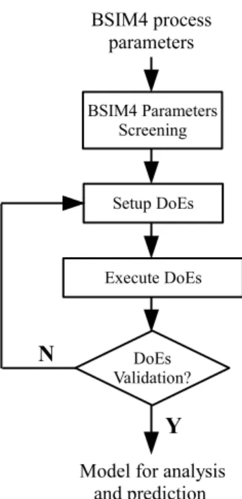
Design of experiments (DoEs) is an information-gathering procedure in statistical analysis. In CMOS circuits and systems design, the purpose of statistical DoEs is to help designers to characterize the impact of the input factors on the output parameters []. We can use it to select and compare process factors (e.g.,BSIM4 parameters) and predict objectives (e.g.,performance parameters). Figure 3 illustrates the detail steps of DoEs. Table 1 shows common applied DoEs in screening and prediction.
DoEs provide several solutions to generate experimental designs for various situations. Commonly used design are the two-level full factorial (contains all combination of different levels of the factors)
and the two-level fractional factorial design (with a fraction such as 12, 14 of the full factorial case, or
other type, e.g.,Plackett-Burman (PB) designs, central composite designs (CCD)).
2 ≤ Number of factors ≤ 4 Number of factors ≥ 5
Screening Full factorial, fractional factorial Fractional factorial, Plackett-Burman
Prediction Central composite, Box-Behnken N/A
Figure 3: DoEs flow: parameter screening, DoEs setup and performance prediction
2.1.1 Parameter screening technology
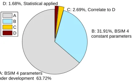
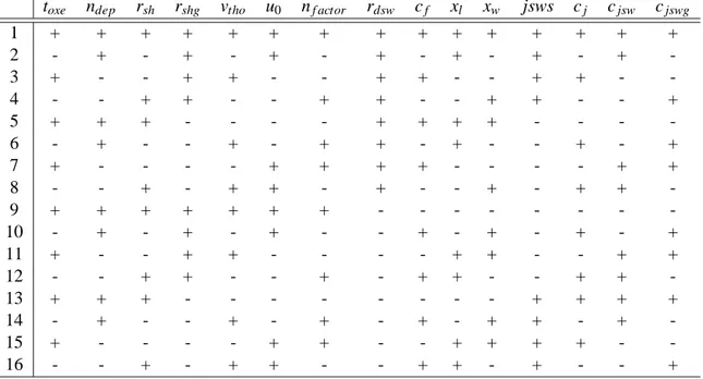
Screening is used to minimize the number of process parameters. Correlation analysis and stepwise regression analysis (execute by Plackett-Burman design) are discussed in this subsection. More than 800 process parameters exist in BSIM4 model (version 4.5). As shown in Figure 4, the total number of parameters in Part C and D is 39. Screening analysis is implemented with:
• Correlation analysis filters out correlated BSIM4 parameters.
• Stepwise regression analysis (Plackett-Burman design) determines the significant order of left
BSIM4 parameters.
Correlation refers to the linear dependence between two variables (or two sets of data). In statistical BSIM4 parameter modeling, correlation analysis is used to filter out correlated BSIM4 parameters. The
correlation coefficientρBi,Bj between two BSIM4 parameters Bi and Bj with expected values µBi, µBj
and standard deviationsσBi andσBj is defined as:
ρBi,Bj = cov(Bi,Bj) σBiσBj = E[(Bi−µBi)(Bj−µBj)] σBiσBj (1)
where E is the expected value operator, cov means covariance. IfρBi,Bj is +1 or -1, the selected two
BSIM4 parameters show a positive (-1 with negative) linear dependence to each other. One of these two BSIM4 parameters can be moved out from model. After correlation analysis, a design of experiments (DoEs) should be selected to verify this new model. To simplify this model, stepwise regression analysis can be applied, results such as p-value from hypothesis testing are evaluated to determine the significant sequence of left BSIM4 parameters.
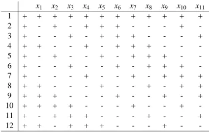
Stepwise regression is used to further minimize the BSIM4 process parameters. According to Ta-ble 1, A two level Plackett-Burman design is selected to execute stepwise regression. Hadamard matrix can generate an orthogonal matrix for input parameters whose elements are all either plus signs or minus signs (Plus signs (+) represent factors with maximum values; minus signs (-) for minimum values). In this case (see Table 2), only 12 runs are needed with Plackett-Burman designs. A full factorial design
A: BSIM 4 parameters under development 63.72% B: 31.91%, BSIM 4 constant parameters C: 2.69%, Correlate to D D: 1.68%, Statistical applied A B C D
Figure 4: The total number of BSIM4 parameters is 893, some parameters (Part A) are still under de-velopment (currently equal to 0 or set to NaN), Part B represents constant BSIM4 parameters which are not influenced by process variations. BSIM4 parameters in Part C and D are proceeded with screening analysis.
In detail, stepwise regression is to build regression models between BSIM4 process parameters (input factors) and performance parameters (objectives) which can make hypothesis testing for models
and every independent input factors. The p-value, partial F-values and R2 value can be used to set a
certain threshold to test the hypothesis of regression model. At each step, the p value of an F-statistic is computed to test models with or without a potential BSIM4 parameter. If a parameter is not currently in the model, the null hypothesis is that the parameter would have a zero coefficient if added to the model. If there is sufficient evidence to reject the null hypothesis, this parameter is enrolled. Conversely, the parameter is removed from the model. Finally, the most optimum regression equation is built with the most significant BSIM4 parameters.
2.1.2 Performance prediction with RSMs
Response surface method (RSM) is another important statistical method to build relationship between input factors (BSIM4 process parameters) and objectives (circuit performance). According to BSIM4 factors distribution, experimental runs are performed with circuit simulator. Central composite design (CCD) is a type of fractorial factorial design can be applied to RSMs. CCD such as circumscribed (CCC), inscribed (CCI) and face centered (CCF) are different in range and rotation of factors. Figure 5 illustrates the distribution of different CCDs with two design factors. Besides three types CCDs, the Box-Behnken design (BBD) is an independent quadratic design which does not contain an embedded factorial or fractional factorial design. Since BBD does not have any combination point at some corner, some applications can benifit from it and avoid some extreme cases.
The simulated performance parameter is used to generate RSMs with BSIM4 parameters [4]. The response surface model can be used for displaying graphically the mathematical model between BSIM4 process parameters and circuit performance. Successive building of RSMs can help designers estimate varied and aged circuit performance efficiently. Sometimes, using linear model is hard to achieve ad-equate accuracy because of exponential complexity, quadratic model or even cubic model is required. The accuracy of RSMs can be evaluated by root-relative-square error (RMSE). It is a measurement for
x1 x2 x3 x4 x5 x6 x7 x8 x9 x10 x11 1 + + + + + + + + + + + + 2 + - + - + + + - - - + -3 + - - + - + + + - - - + 4 + + - - + - + + + - - -5 + - + - - + - + + + - -6 + - - + - - + - + + + -7 + - - - + - - + - + + + 8 + + - - - + - - + - + + 9 + + + - - - + - - + - + 10 + + + + - - - + - - + -11 + - + + + - - - + - - + 12 + + - + + + - - - + -
-Table 2: Screening experiments with Plackett-Burman design: 11 two-level factors for 12 runs.
Figure 5: Comparison of the three type central composite designs
RMSE= s ∑N n=1(Ypredicted,n−Ysimulated,n) 2 N (2) Ylinear=β0+β1X1+β2X2 (3) Yquad= Ylinear+β12X1X2+β11X12+β22X22 (4) Ycubic= Yquad+β112X12X2+β122X1X22+β111X13+β222X23 (5) Number of factor 2 3 4 5 6 7 Full factorial 4 8 16 32 64 128 Fractional factorial (12) 2 4 8 16 32 64 Central composite 9/9 15/15 25/25 25/43 45/77 79/143 Box-Behnken N/A 13 25 41 49 57
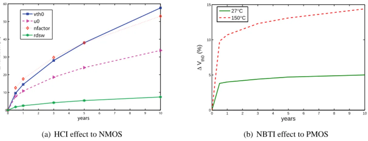
0 1 2 3 4 5 6 7 8 9 10 0 10 20 30 40 50 60 ∆ va ria tio n (%) years vth0 u0 nfactor rdsw
(a) HCI effect to NMOS
0 1 2 3 4 5 6 7 8 9 10 0 5 10 15 ∆ Vth0 (%) years 27°C 150°C
(b) NBTI effect to PMOS
Figure 6: Parameters degradation by ageing effects in NMOS/PMOS transistor, simulating with ELDO.
2.2 Simulation flow
2.2.1 Ageing effects and process variations
In 65nm CMOS technology, ageing effects can degrade some BSIM4 parameters and influence the tran-sistor performance. As shown in Figure 6(a), Hot carrier injection (HCI) can influence sub-threshold
swing coefficient (nf ac), intrinsic threshold voltage (vth0), intrinsic mobility (µ0), saturation velocity
(vsat), drain source resistance per width (rdsw), subthreshold region DIBL coefficient (eta0) and
thresh-old voltage offset (vo f f). The correlation analysis is used to filter out some correlated parameter. vth0,
µ0, nf ac and rdsw are selected as the main degraded parameters of NMOS transistor. Besides, the only
BSIM4 parameter affected by negative bias temperature instability (NBTI) is vth0 of PMOS transistor
(see Figure 6(b)). More severe vth0degradation is observed when PMOS transistor work at high
temper-ature. In Table 4, eight crucial BSIM4 parameters are sorted out as ageing sensitive and non-sensitive.
In NMOS transistor, the dominant ageing nonsensitive BSIM4 parameters include: length variation (xl),
width variation (xw), gate oxide thickness (tox) and channel doping concentration (ndep). In PMOS
tran-sistor, except vth0, other parameters mentioned above are ageing non-sensitive.
Ageing sensitive Ageing non-sensitive
HCI vth0, u0, nf ac, rdsw xl, xw, tox, ndep
NBTI vth0 u0, nf ac, rdsw, xl, xw, tox, ndep
Table 4: Ageing effect to eight BSIM4 parameters
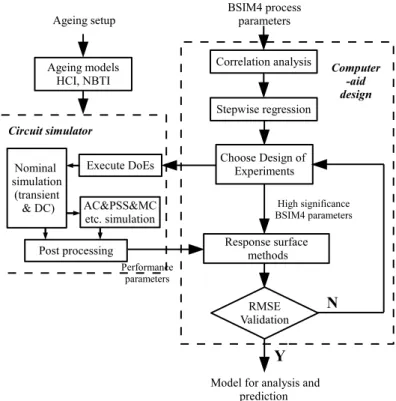
2.2.2 The co-evaluation flow
As shown in Figure 7, this methodology aims to:
• Judge the circuit ageing-immune or ageing-sensitive;
• Estimate degradation of circuit performance due to process variation and ageing effects;
• Find the most critical process parameters.
The flow begins with ageing model selection (HCI and NBTI). The schematic of designed circuit and the stress time are the input of the ageing simulation process. With ageing degradation models, after extracting fresh netlist of designed circuits, a transient simulation is performed to generate a aged circuit netlist. On the branch of process variation, after filter out less important BSIM4 parameters, selected
Figure 7: The co-evaluation flow of ageing effects and process variations
parameters are set up with a proper DoE mode. Ageing effect and process variation are evaluated by cir-cuit simulator. Nominal simulation with transient and DC analysis is performed at transistor level. Other analysis such as AC, PSS and Monte-Carlo can be performed with saved aged circuit netlist (degrada-tion informa(degrada-tion included). Simula(degrada-tion data processing is followed in order to plot response surface. RSMs is used to help designers to obtain intuitionistic reliability information at circuit design phase. For ageing-sensitive circuits, varied RSMs are used to estimate ageing and variability. Meanwhile, for ageing-immune circuits, a fixed RSM can supply variability information to designers [5, 6].
3
Case study
The proposed methodology is applied to two simple current mirrors (NMOS and PMOS type) and dy-namic comparator (see Figure 8). Test circuits are implemented with 65nm CMOS process technology. Minimum transistor dimension is used. Reliability simulation is performed with ELDO simulator (max-imum ageing time = 20 years). HCI and NBTI are considered as the main ageing effects. The statistical flow is carried out with Matlab statistics toolbox. Circuit process variation analysis is based on BSIM4 transistor model.
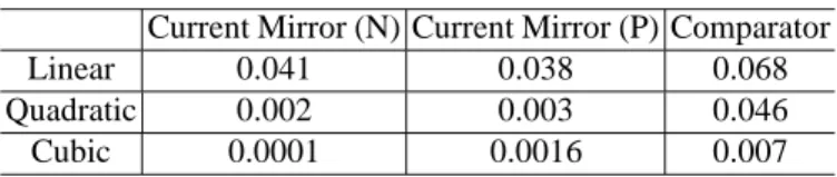
The result from correlation analysis is shown in Table 5. The significant orders determined by regression analysis are shown in Table 6. RMSEs between simulation result and RSMs’ estimation are verified for different models (see Table 7). According to the RMSE results, quadratic model is used to plot RSMs.
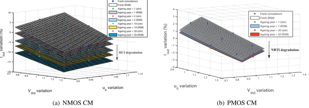
Both NMOS and PMOS simple current mirror have been simulated. The most significant
parame-ters: vth0and u0 are selected and normalized as the representative of process variations. The RSMs are
built between vth0, u0and output current (Ioutas the circuit performance). The ageing analysis indicated
that both HCI and NBTI can degrade output current. Varied response surfaces (see Figure 9(a) and
Figure 9(b)) are used to estimate ageing degradation and process variations (vth0 and u0). Comparing
to HCI induced degradation in NMOS current mirror, the degree of NBTI induced degradation (PMOS current mirror) is lower than HCI.
toxe ndep rsh rshg vtho u0 nf actor rdsw cf xl xw jsws cj cjsw cjswg 1 + + + + + + + + + + + + + + + 2 - + - + - + - + - + - + - + -3 + - - + + - - + + - - + + - -4 - - + + - - + + - - + + - - + 5 + + + - - - - + + + + - - - -6 - + - - + - + + - + - - + - + 7 + - - - - + + + + - - - - + + 8 - - + - + + - + - - + - + + -9 + + + + + + + - - - -10 - + - + - + - - + - + - + - + 11 + - - + + - - - - + + - - + + 12 - - + + - - + - + + - - + + -13 + + + - - - + + + + 14 - + - - + - + - + - + + - + -15 + - - - - + + - - + + + + - -16 - - + - + + - - + + - + - - +
toxe: Electrical gate equivalent oxide thickness
ndep: Channel doping concentration at depletion edge for zero body bias
rsh: Source/drain sheet resistance
rshg: Gate electrode sheet resistance
vtho: Threshold voltage at vbs=0 for long-channel devices
u0: Low-field surface mobility at tnom
nf actor: Subthreshold swing coefficient
rdsw: Zero bias LDD resistance per unit width for RDSMOD=0
cf: Fringing field capacitance
xl: Length variation due to masking and etching
xw: Width variation due to masking and etching
jsws: Isolation-edge sidewall source junction reverse saturation current density cj: Zero bias bottom junction capacitance per unit area.
cjsw: Sidewall junction capacitance per unit periphery.
cjswg: Gate-side junction capacitance per unit width.
Figure 8: Dynamic comparator, transistor dimension W/L = 0.36um/0.06um
Table 6: The significant orders of BSIM4 parameters in test circuits
1 2 3 4 5 6 7 8
NMOS Current Mirror u0 vth0 tox xl nf ac ndep xw rdsw
PMOS Current Mirror vth0 u0 xl tox ndep rdsw nf ac xw
Comparator (NMOS) vth0 tox u0 xw rdsw xl nf ac ndep
Comparator (PMOS) vth0 u0 xl tox rdsw xw ndep nf ac
From the simulation of dynamic comparator, we find the comparator can achieve ageing-immunity with HCI and NBTI stress, not only in offset voltage, also in slew rate and propagation delay of the cir-cuit. Therefore, fixed response surface is used to illustrate the process variation only. The offset voltage is chosen as the circuit performance (see Figure 10(a)). From the regression analysis, we find that the
variations of other parameters except vth0have little or no influence on comparator offset voltage. Thus,
the vth0 is the dominant parameter (see Table 6), in both NMOS and PMOS transistor). Figure 10(b)
shows the fixed response surface which reflect vth0nand vth0pto comparator offset voltage.
References
[1] International Technology Roadmap for Semiconductors. (2009) [Online]. Available:
http://www.itrs.net/Links/2009ITRS/Home2009.htm 0.7 0.8 0.9 1 1.1 1.2 1.3 0.9 0.95 1 1.05 1.1 1.15 −20 −15 −10 −5 0 5 10 u 0 variation V th0 variation Iout va ria tio n (%) Fresh (simulation) Fresh (RSM) Ageing year = 1 (sim) Ageing year = 1 (RSM) Ageing year = 5 (sim) Ageing year = 5 (RSM) Ageing year = 10 (sim) Ageing year = 10 (RSM) Ageing year = 20 (sim) Ageing year = 20 (RSM) HCI degradation (a) NMOS CM 0.7 0.8 0.9 1 1.1 1.2 1.3 1.4 0.9 1 1.1 1.2 1.3 −4 −3 −2 −1 0 1 2 3 4 V th0 variation u 0 variation Iout variation (%) Fresh (simulation) Fresh (RSM) Ageing year = 1 (sim) Ageing year = 1 (RSM) Ageing year = 20 (sim) Ageing year = 20 (RSM)
NBTI degradation
(b) PMOS CM
Table 7: RMSE between simulation and RSMs’ estimation
Current Mirror (N) Current Mirror (P) Comparator
Linear 0.041 0.038 0.068 Quadratic 0.002 0.003 0.046 Cubic 0.0001 0.0016 0.007 0.7 0.8 0.9 1 1.1 1.2 1.3 1.4 0.9 0.95 1 1.05 1.1 1.15 −6 −4 −2 0 2 4 u0 variation V th0 variation Offset variati on (%) Simulation RSM
(a) Vo f f setversus Vth0, µ0
0.7 0.8 0.9 1 1.1 1.2 1.3 1.4 0.8 1 1.2 1.4 −5 0 5 10 15 20 PMOS Vth0 variation NMOS Vth0 variation Offset variation (%) Simulation RSM (b) Vo f f setversus Vth0n, Vth0p Figure 10: Comparator: fixed RSM between BSIM4 parameters and performance
[2] E. Maricau, G. Gielen, ”Computer-Aided Analog Circuit Design for Reliability in Nanometer CMOS” Emerging and Selected Topics in Circ. and Sys., IEEE Transactions on, vol. 1, no. 1, pp. 50–58, 2011.
[3] V. Huard, N. Ruiz, F. Cacho and E. Pion, ”A bottom-up approach for System-On-Chip reliability,”
Microelectronics Reliability, vol. 51, pp. 1425–1439, 2011.
[4] H. Cai, H. Petit, and J.-F. Naviner, ”A statistical method for transistor ageing and process variation applied to reliability simulation” 3rd European Workshop on CMOS variability, pp. 49–52, 2012. [5] H. Cai, H. Petit, and J.-F. Naviner, ”Reliability Aware Design of Low Power Continuous-Time
Sigma-Delta Modulator,” Microelectronics Reliability, vol. 51, no.9-11, pp. 1449–1453, 2011. [6] H. Cai, H. Petit, and J.-F. Naviner, ”A hierarchical reliability simulation methodology for AMS
integrated circuits and systems,” Journal of Low Power Electronics, vol. 8, no.5, pp. 697–705, 2012.
A
p
p
en
d
ix
A
C
o
rr
el
a
tio
n
a
n
a
ly
si
s
o
f
B
S
IM
4
p
a
ra
m
et
er
s
toxe ndep rsh rshg vtho u0 nf actor rdsw cf xl xw jsws cj cjsw cjswg
toxe NaN 0 0 -0.022 0 -0.0045 -0.0197 0 0.0005 0 0 0 0 0 0 ndep 0 NaN 0 -0.016 0 -0.0035 -0.0038 0 -0.1171 0 0 0 0 0 0 rsh 0 0 NaN 0.036 0 -0.0045 0.0378 0 -0.0024 0 0 0 0 0 0 rshg -0.022 -0.016 0.036 NaN 0.0526 0.0065 -0.024 -0.0223 0.1359 -0.0126 -0.0479 0.0129 -0.041 -0.0156 0.0322 vtho 0 0 0 0.0526 NaN -0.0045 0.0226 0 0.0024 0 0 0 0 0 0 u0 -0.0045 -0.0035 -0.0045 0.0065 -0.0045 NaN 0.0205 -0.0125 -0.0908 0.05 0.0045 -0.0125 0.0045 -0.0125 0.0045 nf actor -0.0197 -0.0038 0.0378 -0.024 0.0226 0.0205 NaN 0.0351 0.0892 0.0575 -0.041 -0.0168 -0.0361 -0.0355 0.0226 rdsw 0 0 0 -0.0223 0 -0.0125 0.0351 NaN 0.0226 0 0 0 0 0 0 cf 0.0005 -0.1171 -0.0024 0.1359 0.0024 -0.0908 0.0892 0.0226 NaN 0.3866 -0.2304 -0.0024 0.1219 -0.2366 0.1175 xl 0 0 0 -0.0126 0 0.05 0.0575 0 0.3866 NaN 0 0 0 0 0 xw 0 0 0 -0.0479 0 0.0045 -0.041 0 -0.2304 0 NaN 0 0 0 -0.0018 jsws 0 0 0 0.0129 0 -0.0125 -0.0168 0 -0.0024 0 0 NaN 0 0 0 cj 0 0 0 -0.041 0 0.0045 -0.0361 0 0.1219 0 0 0 NaN 0 0 cjsw 0 0 0 -0.0156 0 -0.0125 -0.0355 0 -0.2366 0 0 0 0 NaN 0 cjswg 0 0 0 0.0322 0 0.0045 0.0226 0 0.1175 0 -0.0018 0 0 0 NaN 1 1