Université de Montréal
Characterization of the radiation field in ATLAS using
Timepix detectors
par
Thomas Billoud
Département de Physique Faculté des arts et des sciences
Thèse présentée à la Faculté des études supérieures et postdoctorales en vue de l’obtention du grade de
Philosophiæ Doctor (Ph.D.) en Physique
mai 2019
Université de Montréal
Faculté des études supérieures et postdoctorales
Cette thèse intitulée
Characterization of the radiation field in ATLAS using
Timepix detectors
présentée par
Thomas Billoud
a été évaluée par un jury composé des personnes suivantes :
Sjoerd Roorda (président-rapporteur) Claude Leroy (directeur de recherche) Jean-François Arguin (membre du jury) Alan Owens (examinateur externe) Sjoerd Roorda
(représentant du doyen de la FESP) Thèse acceptée le :
Résumé
Le travail présenté dans cette thèse porte sur le réseau de détecteurs à pixels ATLAS-TPX, installé dans l’expérience ATLAS afin d’étudier l’environement radiatif en utilisant la tech-nologie Timepix. Les travaux sont rapportés en deux parties, d’une part l’analyse des données recueillies entre 2015 et 2018, d’autre part l’étude de nouveaux détecteurs pour une mise à niveau du réseau.
Dans la première partie, une méthode pour extraire certaines propriétés des MIPs (Mini-mum Ionizing Particles) est développée, basée sur l’étude des traces laissées par ces particules lorsqu’elles traversent les matrices de pixels des détecteurs ATLAS-TPX. Il est montré que la direction des MIPs et leur perte d’énergie (dE/dX) peut être déterminée, permettant d’évaluer leur origine. De plus, la méthode pour mesurer les champs de neutrons thermiques et neutrons rapides avec ces détecteurs est expliquée, puis appliquée aux données. Les flux de neutrons thermiques mesurés aux différentes positions des détecteurs ATLAS-TPX sont présentés, alors que le signal des neutrons rapides ne se distingue pas du bruit de fond. Ces résultats sont décrits dans une publication, et la façon dont ils peuvent être utilisés pour valider les simulations de champs de radiation dans ATLAS est discutée.
Dans la seconde partie, la thèse présente une étude de détecteurs Timepix utilisant l’arséniure de gallium (GaAs) et le tellurure de cadmium (CdTe) comme capteur de radia-tion. Ces semiconducteurs offrent des avantages par rapport au silicium et pourraient être utilisés dans les prochaines mises à niveau du réseau ATLAS-TPX. Comme ils sont connus pour des problèmes d’instabilité dans le temps et une efficacité de collection de charge incomplète, ils sont testés en utilisant divers types d’irradiation. Ceci est décrit dans deux articles, l’un portant sur un capteur au GaAs de 500 µm d’épaisseur, l’autre sur un capteur au CdTe de 1 mm d’épaisseur. Malgré l’apparition de pixels bruyants lors des mesures, les détecteurs montrent une bonne stabilité du signal dans le temps. Par contre, l’efficacité de
collection de charge est inhomogène à travers la surface des détecteurs, avec des fluctuations de produits mobilité-temps de vie (µτ ) importantes. Ces résultats montrent qu’il est nécessaire d’étudier l’influence de ces défauts sur les algorithmes de reconnaissance de traces avant l’utilisation du GaAs et CdTe dans les mises à niveau du réseau ATLAS-TPX.
Mots-clés: mesure de radiation, ATLAS, Timepix, détecteur GaAs, détecteur CdTe
Abstract
The work presented in this thesis focuses on the ATLAS-TPX pixel detector network, in-stalled in the ATLAS experiment for studying the radiation environement using the Timepix technology. The achievements are presented in two parts, on one hand the analysis of data acquired between 2015 and 2018, on another hand the study of new detectors for an upgrade of the network.
In the first part, a method to extract properties of MIPs (Minimum Ionizing Particles) is developed, based on the analysis of clusters left by the interaction of these particles in the pixel matrixes of the ATLAS-TPX detectors. It is shown that the direction of MIPs and their energy loss (dE/dX) can be determined, allowing the evaluation of their origin. Moreover, the method for mesuring the thermal and fast neutron fields is explained, and applied to the data. The thermal neutron fluxes at the different detector locations are reported, whereas the fast neutron signal cannot be distingished from the background. Thoses results are described in a publication, and their use for benchmarking simulations of the radiation field in ATLAS is discussed.
In the second part, the thesis presents a study of Timepix detectors equipped with gallium arsenide (GaAs) and cadmium telluride (CdTe) sensors. These semiconductors offer some advantages over silicon and could be used for upgrades of the ATLAS-TPX network. Since they are known to suffer from time instabilities and incomplete charge collection efficiency, they are tested using several types of irradiation. This is described in two publications, one focusing on a 500 µm thick GaAs sensor, another focusing on a 1mm thick CdTe sensor. Despite the appearance of noisy pixels during the measurements, the detectors are found to be reasonably stable in time. However, the charge collection efficiency is found to be inhomogeneous across the sensor surfaces, with significant fluctuations of mobility-lifetime (µτ ) products. These results show that
it is necessary to study the influence of these material defects on the pattern recog-nition algorithms before the integration of such sensors in the ATLAS-TPX upgrades.
Keywords: radiation monitoring, ATLAS, Timepix, GaAs detector, CdTe detector
Personal contributions
I present here an overview of my work done during the PhD program, which lasted from late 2013 to early 2019 and included two propaedeutic years.
Timeline overview
Having a background in electronics engineering, the first two years of my PhD were mostly dedicated to courses on theoretical and experimental particle physics, and related subjects. In parallel, I contributed to the calibration and installation of the ATLAS-TPX detector network at the Large Hadron Collider (CERN) from 2014 to mid-2015. Soon after, I started my involvement in the ATLAS experiment by performing monitoring shifts for the calorimeter and forward detector systems. These 8 hrs-long shifts were done in the ATLAS control room at CERN. They involved calibration runs, coordination between maintenance activities of the sub-system experts, and continuous surveillance of the detectors’ status and data acquisition during LHC runs. I dedicated about two months per year to this task from 2015 to 2018.
From 2015 to early 2016, I achieved my ATLAS authorship qualification task, which is a required work to become a co-author of the ATLAS collaboration. This involved the analysis of ATLAS-TPX data for luminosity monitoring. My results were used by the ATLAS-TPX luminosity group for publications [1], but are not included in this thesis which focuses on more consequent personal achievements.
From early 2016 to late 2017, my main research activities were related to the characteri-zation of new TPX detectors with CdTe and GaAs sensors, which is the subject of chapter 4. For these investigations, I used the Tandem accelerator of UdeM (University of Montreal), with the help of the responsible technician and ATLAS collaborators, and other radioac-tive sources available at this facility (241
Am,137
Rutherford backscattering setup to irradiate the CdTe Timepix detector with a proton beam at various energies. I also used an X-ray facility at IEAP (Institute of Experimental and Applied Physics in Prague) for detector calibrations and characterizations. There, I exposed fluorescence foils to X-rays in order to obtain mono-energetic sources. I performed analysis of the obtained data with the MAFalda framework. This is a C++ and ROOT [2] based soft-ware developed at UdeM for the Medipix/Timepix community, that unifies several analytical utilities for pattern recognition and integration of user-defined algorithms, but needs to be adapted for specific applications. I extended the program for my purposes and worked on the time-consuming task of writing new algorithms to study the charge collection efficiency in GaAs. This analysis required theoretical and algorithmic developments for taking into account the small pixel effect in the Hecht equation, and for fitting this model to the data recorded by the 65536 pixels of the detector. Based on this analysis, I wrote two articles (included in chapter 4), one addressing the CdTe Timepix detector, and one addressing the GaAs detector. I presented some of the results at a Medipix collaboration seminar at CERN. Finally, in 2018, I focused my research activities on the analysis of ATLAS-TPX data, which is the subject of chapter 3. To characterize the radiation field in ATLAS with these de-tectors, I had to develop new algorithms. Therefore, I created a C++/ROOT based software for convenient comparison between different algorithms and data visualization. In parallel, I began to validate these algorithms using Monte Carlo simulations. Here, I used an open-source software based on Geant4 [3] and specialized for pixel detectors, called Allpix2 [4]. Since this program was developed by a team working on vertex detectors, I had to adapt the code for my needs. The developed algorithms led to successful results from the anal-ysis of the ATLAS-TPX data, that allowed me to write the article included in chapter 3. Preliminary results were presented at the IEEE Nuclear Science Symposium of 2018. The article was submitted for publication to IEEE TNS in February 2019. At the same time of these research activities, I helped with the maintenance of ATLAS-TPX detectors and to the installation of new prototypes (i.e. Timepix3 detectors) tested in 2018 for the future upgrade.
Additional experience
For every code development performed during my research activities, I tried as much as possible to write clean, reusable and publicly available code. This habit can be time-consuming, but it allows to share the acquired experience with the pixel detector community, which can lead to a faster and more efficient technology development. The aforementioned MAFalda and Allpix2 frameworks are tools following this line of thinking. Thus, I integrated my developments to these frameworks whenever appropriate, as can be seen on the public code repositories [5, 6]. In addition, the program I developed for the analysis of ATLAS-TPX data is also accessible on the web [7].
Finally, at the UdeM Tandem accelerator, I performed with ATLAS collaborators ad-ditional measurements with He, Li, C and O ions to investigate the energy resolution and amplifier response of Timepix detectors. In the context of pattern recognition studies, I also participated in measurements at the SPS (Super Proton Synchrotron, CERN), Prague Microtron MT25, and Prague Van De Graaff accelerator (IEAP CTU1
).
Contents
Résumé . . . iv
Abstract . . . vi
Personal contributions . . . viii
List of tables . . . xiii
List of figures . . . xiv
Acronyms . . . xxii
Acknowledgments . . . 1
Introduction. . . 2
Chapter 1. The ATLAS experiment . . . 4
1.1. Status of Particle Physics in 2019 . . . 4
1.2. Proton collisions at the LHC . . . 6
1.3. The ATLAS detector design. . . 8
Chapter 2. The TPX detectors . . . 12
2.1. Particle detection principles . . . 13
2.2. The TPX chip family . . . 17
2.3. Particle interactions in sensors . . . 22
Chapter 3. Radiation field characterization with ATLAS-TPX . . . 33
3.1. Context . . . 33
3.2. Methodology . . . 35
3.3. Publication: Characterization of the Radiation Field in ATLAS With Timepix Detectors . . . 41
3.4. Summary and Beyond . . . 63
Chapter 4. High-Z sensors for ATLAS-TPX upgrades . . . 66
4.1. Context . . . 66
4.2. Methodology . . . 68
4.3. Publication: Characterization of a pixelated CdTe Timepix detector operated in ToT mode. . . 71
4.4. Publication: Homogeneity study of a GaAs:Cr pixelated sensor by means of X-rays . . . 87
4.5. Summary and Beyond . . . 103
Conclusion and Outlook . . . 105
List of tables
2.1.1 Comparison of charge carrier drift times in a 1 mm thick sensor for different materials (see footnote in the text). Mobilities used for the calculation are taken from Ref. [53]. . . 15
3.3.1 Position and operational mode of ATLAS-TPX detectors in the ATLAS cavern. Z is the distance along the beam axis (from the interaction point), R is the radial distance. . . 48
4.3.1 Proton range in Si and CdTe for some energies used in the present study [145]. Semiconductor thicknesses are 300 µm for TPX-Si and 1000 µm for TPX-CdTe. . 77 4.3.2 Comparison of TPX-CdTe and TPX-Si energy measurements for protons of
different energies. Beam energy (Ebeam), beam energy corrected for energy loss
inside the gold foil (ERBS) and energy deposited in the sensor’s active volume
(Ed, corrected for energy loss inside the dead layers using SRIM data [145]) are
reported. Dev is the deviation of Em from Ed and R is the relative resolution.
Bias voltages are −300 V and 100 V for TPX-CdTe and TPX-Si, respectively. . . . 81 4.3.3 TPX-CdTe and TPX-Si energy measurements for X-ray fluorescence sources used
for calibration, 241Am X-rays and 137Cs photopeak (observed only with
TPX-CdTe). Energy deposited in the sensor’s active volume (Ed), measured energy
(Em), deviation of Em from Ed (Dev) and relative resolution (R) are reported.
List of figures
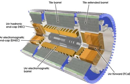
1.2.1 Integrated luminosity recorded by ATLAS as a function of time, during the years after 2010 [36]. . . 7 1.3.1 Overview if the ATLAS detector [11]. . . 8 1.3.2 The ATLAS calorimeter. It is composed of an inner layer for electromagnetic
showers, the LAr barrel, which uses liquid argon (LAr) as active material and lead as absorber. A second outer layer, the Tile barrel, is dedicated to hadronic showers: scintillating tiles were chosen as active component and steel as absorber [11]. In the end-caps and forward regions, additional LAr calorimeters are installed to increase the solid angle coverage. . . 9 1.3.3 The radiation shielding in ATLAS [11]. Shielding components are indicated with
arrows. See text for more details. . . 11
2.1.1 Working principle of a hybrid pixel detector. (a) Standard silicon sensors are doped (p-type on one side, n-type on the other), creating a depletion region at the p-n junction, which must be extended by applying a bias voltage [48]. Sensors are then bump-bonded to a pixelated electronics chip. (b) When a particle interacts in the depletion zone of a sensor, electron-hole pairs are created, and charge carriers move toward the pixel electrodes (e- towards anode, holes towards cathode) under
influence of the electric field [46]. (c) 3D schematics of the pixel detector [46]. . . 14 2.2.1 Illustration of a MPX2 detector [59]. a) Description of the Medipix2 chip and
its sensor. b) Photo of the whole detector with its USB interface (blue box) for connection to a computer. . . 17 2.2.2 Example of frames recorded by a MPX2 detector exposed to 241
Am, 106
Ru, 137
Cs and 10 MeV protons at 0 °(left) and 85 °(right) [60]. Large tracks are due to protons
or to 5.48 MeV α-particles from 241Am, while thin tracks come from electrons (up
to 39 keV from 106
Ru) and photons (662 keV from 137
Cs). . . 19 2.2.3 Image of mouse bones obtained by a MPX2-based detector. The detector is
irradiated by an X-ray tube [61], with the mouse placed in-between. . . 19 2.2.4 Example of frame recorded with a TPX detector exposed to 241
Am, 106
Ru, 137
Cs and 10 MeV protons at 75° [65, 66]. The frame is not full of clusters due to the positioning of the detector compared to the beam and sources. In contrast to figure 2.2.2, the frame has a third dimension (represented in color on the left, and with 3D view on the right), thanks to the TOT mode of the TPX chip. . . 21 2.2.5 120 GeV/c pion track with ejected delta ray recorded by a TPX3 detector [69].
In contrast to figure 2.2.4, the cluster can be represented with a fourth dimension (z-coordinate of the particle trajectory) due to the simultaneous TOT and TOA operation of the TPX3 chip. . . 22 2.3.1 (a) Energy loss of heavy charged particles in different sensor materials. The
stopping power (dE/dx) is calculated using the Bethe-Bloch formula [18]. Multiplying the y-axis by 55 µm, one gets an idea of the deposited energy per pixel if the particle is parallel to the sensor surface. b) Illustration of energy loss measurement by a TPX detector [72]. Here, a heavy charged particle is stopped in the sensor. The measured track reproduce the Bragg curve (shown on the very top). . . 23 2.3.2 2D projections of electron trajectories recorded by a TPX detector irradiated with
a 90
Sr/90
Y radioactive source [73]. . . 24 2.3.3 (a) Simulations of a 2, 5 and 50 MeV electron beam directed at a TPX detector,
equipped with a similar casing than ATLAS-TPX detectors. The detector is irradiated from the back (left side on the pictures), to show the effect of the casing on electron trajectories (red lines). The silicon sensor is the last gray layer on the right, and blue lines represent photons emitted by Bremsstrahlung. (b) Example frames of the 5 MeV and 50 MeV beams, showing the 2D projection of
electron trajectories in the sensor. Simulations were performed using the Allpix2 framework [4]. . . 25 2.3.4 Cross section of photon interactions in TPX sensor materials as a function of
energy [74]. . . 27 2.3.5 (a) Cross section of neutron interactions in silicon [75]. For comparison with
photon cross sections in Si given in figure 2.3.4, the y-axis here must be divided by 50 to obtain σ in cm2
/g. (b) Cross section of neutron absorption in different materials [76]. . . 28 2.4.1 Cluster categories defined in Ref. [60], from investigations with MPX2 detectors.
See text for more details. . . 29 2.4.2 Reconstruction of incident angles using the track shape [79]. . . 30
3.1.1 Picture of an ATLAS-TPX detector. . . 35 3.2.1 Proportion of radiation field components in the region of the TPX01 detector (see
table 3.3.1 for detector position in ATLAS), as obtained from simulations [97]. The y-axis is the number of particles hitting the TPX01 region for 105
proton-proton collisions. To increase statistics, the detector region is taken to be a cut-away ring of the ATLAS cylinder where TPX01 is placed, assuming that radiation fluences are symmetrical around the longitudinal axis. Hence, the particle count is higher than the one actually measured by TPX01 for the same number of proton-proton collisions. . . 36 3.2.2 Spectra of charged particles hitting the location of TPX01 in ATLAS (see
table 3.3.1), as obtained from simulations [97]. On the left spectra, the x-axis is in logarithmic scale. Note the different x-axis range between heavy charged particles (protons, muons, pions), where 1 bin = 1 MeV, and electrons, where 1 bin = 10 keV. . . 37 3.2.3 Side view illustration of the ATLAS-TPX effective area used for the measurement
3.2.4 Example of a frame recorded by ATLAS-TPX, showing the different categories of clusters (see section 2.4): dots (1, 2) and curly tracks (3) originate either from X/γ rays or electrons below their MIP regime, straight tracks (6) come from MIPs and HETEs (4,5) are typical neutron-induced events.. . . 40 3.3.1 The ATLAS-TPX detector [16]. (A) illustrates the detector design and the
principle of discrimination between charged particle and neutron events. (B) shows the segmentation of the sensor surface into the four neutron converter areas, including the free (uncovered) area for background subtraction (see text for more details). (C) gives the dimensions of the detector components and (D) shows the assembled detector unit, which is then placed in a aluminum casing. . . 46 3.3.2 Position of ATLAS-TPX detectors in ATLAS.. . . 47 3.3.3 Description of cluster processing in order to reconstruct charged particles incident
angle and stopping power. t1 and t2 are the thickness of the two Si sensor layers,
300 µm and 500 µm respectively (the subscripts of other cluster properties refer to the corresponding layer). See text for more details. . . 49 3.3.4 Possibilities for wrong direction identification of incident angle according to the
number of sensor layers (diagrams not in scale). With one layer (left), the same cluster can represent 4 particle directions. With two layers (right), the same combination of 2 clusters can represent 2 particle directions only. . . 50 3.3.5 Illustration of detected coincident events for MIPs crossing the hodoscope at
different angles. . . 51 3.3.6 Simulation of an ATLAS-TPX detector irradiated with an isotropic source of
500 MeV pions. (a) The geometry includes the two Timepix chips with their sensors and the neutron converters. (b) The particles are shot with random directions, from a sphere surrounding the detector. . . 53 3.3.7 Reconstructed MIP directions from the simulation described in Fig. 3.3.6. a) Raw
radial axis (θ) represents the incident angle with respect to the sensor surface, as illustrated in Fig. 3.3.4 (θ = 0° means the particle is perpendicular to the surface). 54 3.3.8 Examples of overlapping clusters. a) One MIP emitting δ-rays and b) two MIPs
crossing each other (also with δ-rays). . . 54 3.3.9 Number of HETEs registered per pixel with TPX01 during several LHC runs in
May 2016 (accumulated luminosity: 530 pb-1). HETE locations are determined
from the cluster centroid. The neutron converters placed in-between the two sensor layers are indicated, correspondingly to Fig. 3.3.1. The thermal neutron signal below the LiF+Al converter does not fully cover the delimited area due to the gaps between the different converters. For each pixel, the number of recorded events is incremented when the centroid of a HETE cluster is detected.. . . 55 3.3.10 Thermal neutron fluences per unit luminosity for the different ATLAS-TPX devices
as measured during LHC Fill 4965 on May 31, 2016 (accumulated luminosity: 160 pb-1
) [117]. . . 56 3.3.11 Stopping power (dE/dX) of tracks measured by the ATLAS-TPX detectors with
logarithmic scale (see detector positions in Table 3.3.1). The number of tracks per dE/dX bin is scaled per integrated luminosity. Data were measured during LHC Fill 4965 on May 31, 2016 (accumulated luminosity: 160 pb-1
). . . 58 3.3.12 Stopping power (dE/dX) of tracks measured by the ATLAS-TPX detectors with
linear scale (see detector positions in Table 3.3.1). The number of tracks per dE/dX bin is scaled per integrated luminosity. Data were measured during LHC Fill 4965 on May 31, 2016 (accumulated luminosity: 160 pb-1
). . . 59 3.3.13 MIP directions measured by the ATLAS-TPX detectors (see detector positions in
Table 3.3.1). The radial axis (θ) represents the incident angle with respect to the sensor surface (θ = 0°means the particle is perpendicular to the surface). Data were measured during LHC Fill 4965 on May 31, 2016 (accumulated luminosity: 160 pb-1). . . 61
3.4.1 Birth position of protons (p), muons (µ-), pions (π-) and neutrons (n) hitting the location of TPX01 in ATLAS (see table 3.3.1 for the detector location in ATLAS), as obtained from simulations [97]. The coordinate system origin is the interaction point, on the bottom left corner. The Z-axis is the distance along the beam pipe, and the R coordinate is the cylindrical radial distance. The ATLAS geometry, and consequently, the radiation field, are considered symmetrical around the Z-axis. Note the different scale and binning between charged particles and neutrons. . . 64
4.1.1 Photon detection efficiency as a function of energy for different sensors currently available. The calculation is done for a photon arriving perpendicularly to the sensor surface, with data from Ref. [128]. Displayed sensors can be bump-bonded to either TPX or TPX3. . . 68 4.3.1 Tracks left by a 2 MeV (left) and a 10 MeV (right) proton on TPX-CdTe. The
applied bias is −300 V and protons hit the sensor’s surface perpendicularly. X and Y axes are pixel coordinates. E is the deposited energy per pixel. . . 75 4.3.2 Per-pixel calibration curve for a random pixel of TPX-CdTe. Spectral peaks of Zn
(8.6 keV) and Cd (23.2 keV) fluorescence, 241Am (59.5 keV) X-rays and threshold
energy (6.0 keV) are used for the fit with the ToT surrogate function (eq. 4.3.1). Error bars (errors on the means as calculated by Minuit-Migrad) are not visible. 78 4.3.3 Proton spectra for different energies with a) TPX-Si operated at 100V and b)
TPX-CdTe operated at −300 V. For each figure, the spectra y-axis are scaled according to the lowest energy proton peak. Cluster volumes are computed using each detector’s specific per-pixel calibration, as described in the text.. . . 79 4.3.4 Collected charge (arbitrary units) as a function of bias for TPX-CdTe irradiated
with 800 keV protons. The collected charge is assumed to be proportional to cluster volumes obtained with the per pixel calibration. Error bars (errors on the means as calculated by Minuit-Migrad) are not visible. . . 83 4.3.5 Energy spectra of 5.5 MeV alpha particles as a function of time for TPX-CdTe
bias application. b) Cluster size of 5.5 MeV alpha particles as a function of time for TPX-CdTe exposed to 241Am alpha-particles. . . 84
4.3.6 The behaviour of the effective bias with time, calculated from the dependence of the cluster size on time and bias.. . . 84 4.3.7 Response of TPX-CdTe to X-rays from Cd fluorescence. a) Total number of
single pixel clusters. b) Average energy of single pixel clusters. The detector was operated at −300V during ∼45 mn with an acquisition time of 1 ms. . . 85 4.4.1 a) IV curve of the GaAs:Cr sensor obtained with a Keithley source meter at room
temperature, with a linear fit and the resulting resistance. b) Penetration curves (black) of 8 keV, 23 keV and 60 keV X-rays in a 500 µm thick GaAs layer and weighting potential [56] (red) for a charge carrier traveling along the center of a pixel. I(x)/I(0) is the fraction of photons left at a depth x in the sensor from an
incoming intensity I(0).. . . 91
4.4.2 X-ray spectrum of the 8 keV (a) and 23 keV (b) source obtained from Cu and Cd fluorescence emission, respectively, using the per-pixel calibration. Only single pixel hits are taken into account. Gaussian fits are displayed in red, along with the fit parameters. . . 92 4.4.3 a) Total TOT (summed over 1000 frames) as a function of time for the 23 keV
source with a -300 V bias. The black graph includes all pixels whereas the red graph excludes 3 lines of pixels on each border of the detector. b) Average TOT of single pixel hits as a function of time for the same measurement, illustrated with two different time scales. . . 94 4.4.4 Map (a) and distribution (b) of hit counts per-pixel for the 23 keV X-ray irradiation
at -300 V. The dashed area on the map is enlarged in figure 4.4.5. . . 96 4.4.5 Zoom on the dashed area of figure 4.4.4 a) with pixel spectra from different regions.
Gaussian fits are displayed in red, along with the fit parameters. The detector is operated in TOT mode, which allows the measurement of deposited energy and photon counting at the same time. . . 97
4.4.6 Map of Gaussian means (in TOT) for the 23 keV irradiation with a bias of -300 V (a) and -30 V (b). Examples of fitted Gaussian functions are illustrated in red in figure 4.4.5 for -300 V. . . 98 4.4.7 a) Correlation between the photon count map and the Gaussian mean map for the
23 keV irradiation at -30 V (left) and -300 V (right). Each bin corresponds to the number of pixels with a specific Gaussian mean and photon count. b) Comparison of Gaussian mean distributions with calibrated and uncalibrated data for the 23 keV irradiation at -300 V. . . 98 4.4.8 µeτe map (a) and distribution (b) obtained from the 23 keV source. The dashed
area on a) is enlarged in figure 4.4.9 a). . . 100 4.4.9 a) Hecht graphs and fit functions for the same pixels as figure 4.4.5. For each point,
the error bar was calculated from the statistical errors on the TOT Gaussian mean and calibration coefficients. b) Zoom on the dashed area of figure 4.4.8 (same area as figure 4.4.5). The arrow colors refer to the graphs on the left. . . 101 4.4.10 Correlation between the photon count map at -300 V and the µeτe map for the 23
keV irradiation. Each bin corresponds to the number of pixels with a specific µeτe
and photon count. . . 101 4.5.1 Birth position of photons hitting the location of TPX01 in ATLAS (a) and their
spectra (b), as obtained from simulations [97]. See table 3.3.1 for the detector location in ATLAS. See figure 3.4.1 and 3.2.2 for comparisons with charged particles and neutrons. . . 104
Acronyms
ASIC: Application-Specific Integrated Circuit CCE: Charge Collection Efficiency
CERN: Centre Européen de la Recherche Nucléaire
IEAP: Institute of Experimental and Applied Physics in Prague IP: Interaction Point
MIP: Mimimum Ionizing Particle MPX2: Medipix2
PCB: Printed Circuit Board SPS: Super Proton Synchrotron TPX: Timepix
TPX3: Timepix3
Acknowledgments
First, I would like to warmly thank my PhD supervisor, Prof. Claude Leroy, for his support in my research activities and for his guidance in general.
At the University of Montreal, I have been helped with several colleagues for experimental setups. I annoyed the technician operating the Tandem accelerator a lot, so I thank Louis Godbout for his patience. I performed many measurements with the help of a PhD mate, Costa Papadatos, and gave a hard time to Jean-Samuel Roux (BSc. student) for help with code development. During my PhD experience at the GPP2
group of UdeM, I have had a feeling of professionalism and consideration, to which Jean-François Arguin and Peggy Larreau contributed.
At IEAP (Prague), I have received a lot of experimental support and expertise from Benedikt Bergmann and Martin Pichotka. I am grateful to the former institute director Stanislav Pospisil, for his welcome and plentiful scientific advices, and to his successor, Ivan Stekl, for continuing to trust in me. The engineering team were also very supportive for detector related purposes, in particular Ing. Yesid Mora.
Finally, I am grateful to my girlfriend, Roxane Martz, for following me to Canada and to my parents, Evelyne Boguet and Pierre Billoud, for their continuous support.
Introduction
Collider experiments require high collision rates, i.e. high energies and luminosities, to investigate physics beyond the Standard Model. The LHC is currently the largest accelerator worldwide, providing about a billion proton-proton collisions per second at a center-of-mass energy of 13 TeV. Despite the exciting discovery potential provided by this achievement, experiments face serious challenges in terms of performance, lifetime and maintenance of their detectors. Indeed, the harsh radiation environment generated by collisions induces high levels of background, radiation damage to electronics and sensors, and induced radioactivity. This was known long before LHC operation, and studies of the radiation field contributed to the design of LHC experiments [8]. For ATLAS, Monte Carlo simulations were performed during more than two decades in order to obtain a detailed knowledge of the expected radiation environment, before the start of the LHC operation in 2008 [9, 10].
Even though simulation tools can predict detailed properties of particle fields at any location in the experiment, actual measurements must be performed once the accelerator has started providing collisions. In ATLAS, several monitors were installed in detector systems particularly affected by the adverse effects of radiation, such as in the inner detector or the muon chambers [11]. While serving their purpose, these monitors only see localized parts of the radiation environment and are typically sensitive to one type of radiation only. In the 2000s, a new particle tracking technology emerged from the Medipix collaboration at CERN, called the Timepix detectors. These are small hybrid pixel detectors capable of measuring charged particles, photons and neutrons at the same time, using a sensor that can be made of several semiconductors such as silicon, GaAs or CdTe. In view of their success as radiation monitors in other applications, it was decided to install a network of such devices [12] at various positions in ATLAS to characterize the radiation field from a more global perspective as other detectors do. A first network, ATLAS-MPX [13], operated
during LHC Run-1 (2010-2013) [14], and was upgraded for the LHC Run-2 (2015-2018) [15] using more recent chip generations. This network upgrade, ATLAS-TPX [16], is the subject of the present thesis. Both analysis of the data obtained during LHC Run-2 and possible future upgrades are investigated.
The first chapter briefly describes the overall context of the ATLAS experiment, with its physics goals and its design. The second chapter is an introduction to particle tracking with Timepix detectors, encompassing general particle detection principles, chip descriptions and data analysis tools. The two last chapters contain the achievements of the thesis. They were submitted in three separate papers (two published, one being reviewed), which are included in their entirety and accompanied with explanatory sections. The third chapter presents results obtained from the ATLAS-TPX network, with discussions about their potential for radiation simulation benchmarking. Finally, the fourth chapter is a preliminary investigation of Timepix detectors with high-Z sensors, which have been available only recently and could be used together with Timepix3 chips for the next upgrade of ATLAS-TPX.
Chapter 1
The ATLAS experiment
1.1. Status of Particle Physics in 2019
If Aristotle’s ideas about the fundamental constituents of nature were not challenged by the curiosity of others, we would think that everything is made of earth, water, air and fire. Luckily, this rather philosophical question has occupied many minds over the centuries. Democritus brought forth the idea of indivisible atoms in the 4th
century BC, but we had to wait more than twenty centuries for a real scientific breakthrough. Some of the standing out initiators of that breakthrough, at the end of the 19th century, are J. Dalton with his investigation on elemental weights, and J.J. Thomson who separated the electron from the heavier part of matter. Soon after, Rutherford, Geiger and Marsden revealed this heavier part of matter with their famous gold foil experiments, establishing a first milestone in the understanding of the fundamental constituents of matter. Further research in this topic then emerged as particle physics for some, and nuclear physics for others, encompassing several methods such as particle accelerators and related detectors, which is the context of the present thesis.
The origin of this scientific area can be traced back to the 1930s, when experimental physicists investigating elementary particles could not be satisfied anymore by radioactive and cosmic ray sources [17]. They expressed the need for intense beams of energetic particles, which was materialized for example with the Cockroft-Walton Generator, one of the first particle accelerators. During the following decades, the development of such machines led to regular discoveries of elementary particles, following the evolution of achievable energies and collision rates. The milestones achieved were also the result of detector development,
adapted to the increasing energies available, making access to smaller constituents possible and allowing study of their properties and interactions. By the 1970s, the accumulation of these discoveries led to the establishment of a solid theory of fundamental interactions and particles called the Standard Model [18] (SM). Since then, several predictions of the model have been confirmed, such as the top quark in 1995 [19] or the tau neutrino in 2000 [20]. The last expected milestone was the discovery of the Higgs Boson, which was achieved in 2012 by the ATLAS and CMS experiments at CERN1
[22, 23]. However, it has been suspected, since its inception, that the SM is not a complete theory. The simple fact that the theory is built upon arbitrary parameters, for example, raises the suspicion of theorists [24]. One might also wonder whether quarks and leptons really are elementary particles [25]. In addition, several experimental observations revealed inconsistencies with the SM. For example, neutrino oscillations experiments showed that neutrinos have a mass, contrary to the SM where they are massless, and a series of astrophysical and astronomical observations lead to the hypothesis of dark matter and dark energy, not predicted by the SM.
To answer these questions, high energy accelerator experiments are still considered as a tool-of-choice nowadays. Currently, the terra incognita explorer of accelerator physics is the Large Hadron Collider (LHC) at CERN [26], a storage ring accelerating two proton beams colliding at a maximum center-of-mass energy (√s) of 13 TeV. Now that the Higgs boson has been confirmed, an important focus is directed towards physics beyond the SM, including supersymmetry and other theories such as composite quark models, extra dimensions or the grand unified theory [27]. Since the LHC has the highest energy ever achieved by an accelerator to date, unexpected findings are also possible. The accelerator gave first collisions at √s = 7 T eV in 2010 [28], and is now in a shutdown period (2019-2020) to upgrade its injector. Its last main upgrade will be the High-Luminosity-LHC (HL-LHC), which should operate from 2027 to 2037 with a significantly higher luminosity and an energy reaching √
s = 14 T eV [29, 30]. Extensive efforts are being invested in this project, with about 7,000 scientists [29] working on the four main experiments (CMS, ATLAS, ALICE, LHCb), and
1Centre Européen pour la Recherche Nucléaire, increasingly called the European Laboratory for Particle
new analytical tools (e.g neural networks) are being developed to confront the huge amount of recorded data. Unfortunately, no evidence of new physics has been found so far [27].
For the future, one hope of the particle physics community is that still increasing accel-erator energies and luminosities will lead to findings beyond the standard model. Various projects are ongoing or considered around the world [31, 32]. However, the resources needed for such infrastructures are reaching a point where it becomes difficult to convince the pub-lic [33]. In this regard, it is important to remember that accelerators are not the only way of studying high energy particles. Indeed, space physics is also a very active field, with sophisticated detection systems being built continuously.
1.2. Proton collisions at the LHC
The LHC is a synchrotron-type accelerator of 27 km circumference. Before they enter the LHC, protons are pre-accelerated by a chain of 4 accelerators, reaching 450 GeV in the Super Proton Synchrotron (SPS). They are transfered to the LHC rings bunch by bunch, and then further accelerated by superconducting magnets. The center-of-mass energy was increased gradually up to 8 TeV during LHC Run-12
(2010-2013), and ramped up to 13 TeV for the LHC Run-2 (2015-2018). Nominally, a LHC beam can contain 2808 bunches of 1011 protons
each, squeezed so that there can be about 20 collisions per bunch crossing [34]. During Run-2, the LHC went beyond the nominal performance, reaching an average of 37 collisions per bunch crossing [15]. This determines the achieved instantaneous luminosity (L ), a key parameter for an accelerator representing its collision rate performance. Considering an interaction with cross section σ, one can calculate the rate of events (R) with:
R = L · σ (1.2.1)
The total cross section for inelastic proton-proton collisions at 13 TeV being ∼ 70 mbarns [35], the LHC produced during its 2018 luminosity peaks (L ∼ 2·1034cm-2s-1) about 109 collisions
every second. In order to study rare processes, one needs to obtain a maximum integrated luminosity over time, which requires high instantaneous luminosity and a continuous opera-tion of the accelerator. Since the number of protons in each beam decreases while collisions
2A LHC Run is a continuous operation of the LHC over the years, followed by a long shutdown during
which major upgrades are done on the accelerator and detectors. The LHC Run-1 period was 2010-2013, Run-2 was 2015-2018 [14, 15]. A daily collision period, with start/stop of the machine, is called a fill.
Month in Year
Jan Apr Jul Oct
] -1 Delivered Luminosity [fb 0 10 20 30 40 50 60 70 80
ATLAS Online Luminosity
= 7 TeV s 2011 pp = 8 TeV s 2012 pp = 13 TeV s 2015 pp = 13 TeV s 2016 pp = 13 TeV s 2017 pp = 13 TeV s 2018 pp 2/19 calibration
Fig. 1.2.1. Integrated luminosity recorded by ATLAS as a function of time, during the years after 2010 [36].
go on, the collision rate decreases accordingly, and when the instantaneous luminosity is no longer deemed sufficient, beams are dumped and new ones are injected. The delivered luminosity3
is illustrated in figure 1.2.1, showing the operation and performance of the LHC over the years.
While the ever increasing luminosity improves the discovery potential, it results in serious challenges for detector lifetime and performance. Each proton-proton collision produces hundreds of secondaries (including neutrons), which interact in the surrounding materials and create subsequent radiation such as the gamma fields related to induced radioactivity. This radiation environment has various deleterious consequences, which require a careful detector design. Indeed, it is important to 1) detect physics processes successfully and 2) allow the experiment to survive these adverse conditions during the entire LHC runs.
3The delivered (or integrated) luminosity is the integration of the instantaneous luminosity over time
and is usually given in inverse barn, instead of cm-2. One barn is equal to 10-24cm2. In the figure, the
Fig. 1.3.1. Overview if the ATLAS detector [11].
1.3. The ATLAS detector design
At the LHC, two general-purpose experiments were proposed to investigate new physics, each with a specific design [37]: ATLAS and CMS. The main conceptual differences are in the magnet systems, used for identifying charged particles and measuring their momenta by bending their trajectories. CMS stands for Compact Muon Solenoid: one solenoidal magnet deflects both highly interacting particles, stopped in the calorimeters, and energetic muons, which have low stopping power and escapes further away. ATLAS (A Toroidal LHC Apparatus), on the other hand, has two magnets: one core solenoid, and one large outer toroid dedicated to escaping muons. Shaped as a 44 m long cylinder with 25 m radius, the ATLAS experiment contains 7000 tonnes of material which is shared between detection systems and their radiation shieldings.
1.3.1. Sub-detectors
The ATLAS detector is thoroughly described in Ref. [11]. An overview of its structure is illustrated in figure 1.3.1. It is composed of cylindrical sub-detector layers added on top
Fig. 1.3.2. The ATLAS calorimeter. It is composed of an inner layer for electromagnetic showers, the LAr barrel, which uses liquid argon (LAr) as active material and lead as ab-sorber. A second outer layer, the Tile barrel, is dedicated to hadronic showers: scintillating tiles were chosen as active component and steel as absorber [11]. In the end-caps and forward regions, additional LAr calorimeters are installed to increase the solid angle coverage.
of each other, in a similar way as onion layers, which can be grouped in three main parts listed below in order of proximity to the interaction point (IP):
• the inner tracker: high spatial granularity for precise trajectory reconstruction. It is composed of a pixel detector, a strip detector and a transition radiation tracker (see figure 1.3.1).
• the calorimeter: heavy absorber materials for stopping most particles and active materials for measuring their energy. See figure 1.3.2 and its caption for a more detailed description. It is surrounded by the solenoid magnet.
• the muon system: gas-filled detection chambers integrated with the toroidal magnet. Even though each particle interacting in those detectors produces a signal, electronic readouts are not capable of recording all proton-proton collisions during the bunch spacing time. Consequently, the experiment is equipped with a trigger system that filters events of interest for physics analysis. This system takes information from various detector sub-components
as input, and performs online computations to select desired data. Finally, four independent detectors are placed in the forward regions:
• LUCID (LUminosity measurement using Cerenkov Integrating Detector). It monitors the online luminosity, and is calibrated using measurements from other detectors [38]. • ALFA (Absolute Luminosity For ATLAS), scintillating fiber trackers placed in Roman pots that can move as close as 1 mm to the beam [39]. It measures the absolute luminosity, and is calibrated during dedicated Van-Der-Mer scans.
• AFP (ATLAS Forward Proton detector), tracking detectors also placed on Roman pots, to measure momentum and emission angle of forward protons [40].
• ZDC (Zero-Degree Calorimeter), calorimeter detecting forward neutrons and photons in both proton-proton and special heavy-ion collision runs [41].
1.3.2. Shielding
In addition to detector systems and associated magnets, radiation shieldings also con-tribute significantly to the overall experimental weight, adding up to 2825 tons. The purpose of shielding is to protect sensitive detectors from the deleterious effects of radiation and has to be specifically designed, as will be discussed in more detail in chapter 3. The main shield-ing components in ATLAS are illustrated in figure 1.3.3. They were optimized by takshield-ing into account the regions where most of the radiation comes from: the IP, the beam pipe, the forward calorimeter (FCal) and the TAS collimator (Target Absorber Secondaries, which prevents the first LHC quadrupole from quenching due to radiation) [42]. The main shield-ing components were made up of three layers, each designed to stop a specific field of the radiation environment: 1) an iron or copper layer to stop energetic hadrons, 2) a boron-doped polyethylene layer to moderate and absorb neutrons, and 3) a steel or lead layer to stop photons originating from radioisotopes created in the second layer [42]. The moderator shielding is placed on the front side4
of FCal and the end-caps, which are an intense source of background radiation [42]. On their backside, the Calorimeter shielding (tailored blocks fill-ing small available spaces) and disk shieldfill-ing protect the end-cap muon inner station. The toroid shielding sits just behind the disk shielding and has an additional protection layer around the beam-pipe. The forward shielding protects the middle and outer end-cap muon
Fig. 1.3.3. The radiation shielding in ATLAS [11]. Shielding components are indicated with arrows. See text for more details.
stations from radiation originating from the beam pipe and TAS. Finally, the nose shielding is an extra protection to globally reduce the impact of radiation from the TAS on the overall experiment.
Chapter 2
The TPX detectors
In the 1990s, the WA97 experiment at CERN investigated the quark-gluon plasma filling the universe during the quark epoch, which lasted from 10-12s up to 10-6s after the big bang
bang. To detect the products of lead-lead collisions provided by the SPS with fine spatial granularity, it was decided to develop a tracking system using a new technology. This led to the design of pixelated readout chips which can be bonded to any type of sensor (e.g. Si, GaAs, CdTe, gas), with the aim of detecting individual radiation quanta with minimal noise. This technology was called hybrid pixel detectors1
[43]. Soon, it was realized that the con-cept had a potential for applications beyond accelerator experiments, for example medical imaging, radiation background monitoring or space physics. It was then that the Medipix collaboration was born, pooling the forces of several institutes aspiring to a widespread tech-nology transfer [44]. Gaining a high degree of success over the years, it was decided to branch the development of hybrid pixel detectors in two directions: Medipix, a chip initially devel-oped as a single photon counting detector with medical applications in mind, and Timepix, a general purpose chip for radiation tracking [45]. Among the various versions available today, three will be discussed in the context of the present thesis: Medipix2 (or MPX2 ), Timepix (TPX ) and Timepix3 (TPX3 ). The chapter starts with a general description of radiation detection with pixel detectors and of the various readout ASICs used throughout the thesis. Then, the related physics of particle interaction in matter is presented, followed by a section on the data analysis tools used for particle tracking.
1the term hybrid is used in opposition to monolithic pixel detectors, which are produced differently:
2.1. Particle detection principles
As for many other radiation detector types, the physical feature exploited with pixel detectors is the fact that ionizing energetic particles create electron-hole pairs along their path in matter that can induce a detectable signal on electronic circuitry. A pixel detector is composed of two parts: a sensor and a readout chip. The sensor is the part sensitive to particle interactions, where charge carriers create a signal, and the readout is where the signal is shaped, allowing the physicist to perform his interpretations. A rich set of physical laws and properties encompass the working principles of the sensor, while the electronic readout design is an engineering challenge. This is thoroughly described in text books such as Ref. [46]. In this section, I summarize the concepts that are directly related to topics discussed in later chapters, and provide graphs illustrating the behavior of Medipix/Timepix detectors used in practice.
2.1.1. Charge carriers in a sensor
Charged particles interact all the way along their path in matter by Coulomb scattering with atomic electrons. The amount of scattering per unit distance, and how neutral parti-cles can also be detected, are the subjects of section 2.3. Coulomb interactions create free electron-hole pairs within the semiconductor, or charge carriers, that must travel towards electrodes in order to induce a signal. This is achieved by applying a bias voltage to a cus-tomized semiconductor piece, which must have limited leakage current in order to minimize the dark signal. The most common sensors are reverse biased diodes made of silicon, while Schottky diodes or ohmic contact sensors are becoming increasingly available with compound semiconductors (e.g. CdTe, GaAs) [47]. A pixel detector is made by tailoring semiconductor junctions to a matrix of electrodes on one side of the sensor, that is then bump-bonded to the electronic readout (or chip). The other side of the sensor is covered by a common electrode, called the backside electrode2
. The working principle of a pixel detector is summarized in figure 2.1.1.
When electron-hole pairs are released by a particle interaction, they start to move under the influence of competing phenomena. First, when a high charge carrier density is created,
2Note that this name can be misleading, because most of the time one puts this side of the sensor in
(a)
(b)
(c)
Fig. 2.1.1. Working principle of a hybrid pixel detector. (a) Standard silicon sensors are doped (p-type on one side, n-type on the other), creating a depletion region at the p-n junction, which must be extended by applying a bias voltage [48]. Sensors are then bump-bonded to a pixelated electronics chip. (b) When a particle interacts in the depletion zone of a sensor, electron-hole pairs are created, and charge carriers move toward the pixel electrodes (e- towards anode, holes towards cathode) under influence of the electric field [46]. (c) 3D
it is subjected to a plasma effect, delaying the signal induction [49]. This is accompanied by a funneling effect, describing the fact that carriers in the center of the plasma are pulled toward the collecting electrode [50]. In parallel, thermal diffusion of the carrier cloud and its drift motion under the electric field occur simultaneously, making carriers spread while they move towards the electrode. Consequently, when pixels are small, carriers can spread to the neighboring electrodes, leading to a signal on several adjacent pixels (cluster). This is called the charge sharing effect, and it has already been studied with TPX detectors [51, 52].
The drift velocity of charge carriers depends on both the carrier mobility, which varies among sensor materials, and the applied bias. A comparison of drift times in TPX sensors available in practice3
is given in table 2.1.1. It can be noticed, for example, that GaAs has
mobility (cm2
V-1
s-1
) drift time (ns) for 1mm @300V
Si e- 1500 22 holes 480 69 GaAs e- 8500 4 holes 400 83 CdTe e- 1050 32 holes 100 333
Tab. 2.1.1. Comparison of charge carrier drift times in a 1 mm thick sensor for different materials (see footnote in the text). Mobilities used for the calculation are taken from Ref. [53].
the fastest electron collection time, which is of interest for applications where the particle time stamp is measured. However, it is known that compound semiconductors such as GaAs and CdTe suffer from carrier trapping centers, which block carriers before they have fully induced the signal. This is explained in more details in the following section.
3The comparison here is given for a 300 V bias, which is slightly above typical values for Si (to avoid
breakdown, i.e. when the sensor becomes conductive). On the contrary, at room temperature, TPX detectors made of recent 1 mm GaAs and CdTe sensors can usually be operated successfully up to ∼ 500 V.
2.1.2. Signal induction
When charge carriers move inside the sensor, they induce a voltage pulse in the pixel electrodes, that is then amplified by the electronic circuitry of the chip. This voltage pulse does not appear at the time when the carriers reach the electrode, but rises as soon as the carriers start to move inside the sensor volume. The charge induced by a carrier moving from depth x1 to x2 in the sensor can be calculated from the Ramo theorem [54, 55], giving [46]:
Q(x) = e(φ(x1) − φ(x2)) (2.1.1)
where e is the elementary charge and φ(x) the so-called weighting potential. Even though equation 2.1.1 looks straightforward, the calculation of the weighting potential for a pixel detector is not, and depends on the electrode geometry. Using the expression derived in Ref. [56], the weighting potential affecting a charge carrier traveling along a straight path in the center of a pixel volume, for the TPX pixel size with a standard 300 µm thick sensor, is shown in figure 4.4.1 (c.f. publication in section 4.4). Interestingly, a consequence of this relation is that carriers induce most of the charge when they travel close to the pixel electrode, which is commonly referred to as the small pixel effect [57]. Moreover, it can be noted that only one carrier type (either electron or hole) significantly contributes to the signal, depending on the applied bias polarity. A last remarkable consequence is that the weighting potential for neighboring pixels also fluctuates as function of depth in the sensor, even though it starts and ends at 0, resulting in no net induced charge. Since pixel amplifiers are sensitive to voltage fluctuations (either positive or negative), they will record part of the induced voltage on neighboring pixels, thus adding an extra component to the overall signal: this is called the transient signal [57]. Combined with the charge sharing effect described earlier, this can result in signals spread over a large number of pixels (cluster).
For fully depleted silicon sensors, the induced charge is, to a good approximation, equal to the amount of charge carriers created by the interaction of the particle. This is not the case, however, with compound semiconductors, because they usually suffer from abundant charge carrier trapping centers. Since carriers induce the signal while they move towards the electrode, they will stop contributing when they are trapped. This results in the deterioration of energy resolution and cluster morphology, and, in the worst case, to an absent signal. To quantify this effect, an average lifetime is attributed to electrons and holes in the material,
(a) (b)
Fig. 2.2.1. Illustration of a MPX2 detector [59]. a) Description of the Medipix2 chip and its sensor. b) Photo of the whole detector with its USB interface (blue box) for connection to a computer.
representing the time during which they drift before they are trapped. When assessing the quality of a compound semiconductor, a common parameter to measure is the mobility-lifetime product (µτ ). This parameter allows one to get an estimate of the maximum sensor thickness that can be used to obtain a reasonable charge collection efficiency (CCE). The CCE is the ratio of the induced charge to the charge deposited originally by the incident particle in the sensor. It is given by the Hecht equation [58], which is used in practice to extract the µτ product of either electrons or holes depending on the bias polarity.
2.2. The TPX chip family
2.2.1. Common properties
The MPX, TPX and TPX3 chips are 2 cm2 ASICs subdivided into 256 x 256 pixels with
a 55 µm pitch4. The chip is bump-bonded to a sensor, most commonly 300 µm silicon, and wired to a PCB as shown in figure 2.2.1a. The PCB is connected to a USB interface (blue box in figure 2.2.1b), allowing connection to a computer for detector control, data acquisition
4except the oldest chip Medipix1, which has not been used in the present work and is therefore not
and visualization. The detector fits in a hand and can be easily positioned in a wide range of experiments, or integrated in larger particle tracking systems. Each pixel has its own electronic circuitry (e.g. clock, shutter, digitizer), meaning that a chip is in fact made of 65536 independent detectors. Data can be recorded in different modes depending on the chip version, as described below.
2.2.2. Medipix2
The Medipix2 chip is available since 2005 [45]. It was used in the ATLAS-MPX net-work (operated in 2008-2012), predecessor of the ATLAS-TPX radiation monitoring system presented in chapter 3. Pixels are active during constant acquisition time intervals called frames, which can be adjusted according to particle fluxes. Frames can be viewed as images of incoming radiation, interspersed by a dead time depending on the amount of readout data. Each pixel can count the number of times it has been hit by an interacting particle: this is called the counting mode. During a frame, the hit count is incremented each time the input charge induced on the pixel amplifier reaches a threshold, which can be tuned to select different energy ranges. If the acquisition time is short enough, the frame is composed of pixel clusters, each cluster corresponding to one particle interaction. This is illustrated in figure 2.2.2 with frames recorded by a MPX2 detector exposed to various sources of radiation. The cluster shape depends on the particle type, energy and direction, as will be discussed in the next section. In cases where high statistics is required, e.g. for medical imaging or luminosity measurement in LHC, one chooses a longer acquisition time to reduce the dead time. This is illustrated, in figure 2.2.3, with an X-ray image (integration of multiple frames) of mouse bones obtained with a MPX2-based detector. The detector used for this image is a matrix of 2x2 MPX2 chips connected together side by side. Here, the pixels count the number of photons that go through the mouse during the exposure time.
2.2.3. Timepix
With the release of TPX in 2007, it became possible to measure the energy deposited by particles in the sensor and their timestamp. While the ASIC is still based on a frame-by-frame readout, two modes of operation were added, the TOT mode and the TOA mode. ToA means Time Of Arrival: during a frame, when a pixel is hit by a particle, the timestamp is recorded. The reference clock can be set up to 100 MHz [62], resulting in a 10 ns time
Fig. 2.2.2. Example of frames recorded by a MPX2 detector exposed to241
Am,106
Ru,137
Cs and 10 MeV protons at 0 °(left) and 85 °(right) [60]. Large tracks are due to protons or to 5.48 MeV α-particles from 241
Am, while thin tracks come from electrons (up to 39 keV from
106
Ru) and photons (662 keV from137
Cs).
Fig. 2.2.3. Image of mouse bones obtained by a MPX2-based detector. The detector is irradiated by an X-ray tube [61], with the mouse placed in-between.
granularity5
. TOT means Time Over Threshold: during a frame, each pixel records the time during which the input charge is above a predefined threshold. The higher the TOT value, the higher the energy. To obtain a good energy resolution, a standard method is to perform a per-pixel calibration using X-ray irradiation. It has been found [63] that the relation between TOT and deposited energy (E) is non-linear for energies close to the threshold (t):
T OT(E) = aE + b −
c
E − t (2.2.1)
Using several X-ray sources, typically from 6 keV to 60 keV, the four parameters (a,b,c,t) can be extracted [64]. The threshold is adjustable, and is usually set to its minimum (around 3 keV for silicon sensors) for best particle tracking performance.
As for MPX2, the TPX detector can thus perform particle tracking, with either its counting, TOT or ToA mode. Nevertheless, the TOT mode adds a significant advantage compared to MPX. Indeed, with this mode, pixel clusters contain the deposited energy and can be represented with a third dimension, as shown in figure 2.2.4. This allows to achieve sub-pixel spatial resolution, stopping power measurements and better particle categorization, as will be discussed in the next section. The TPX chip is the technology used in the ATLAS-TPX network, which is the topic of chapter 3.
2.2.4. Timepix3
TPX3 is currently the latest available version of the Timepix family, even though its successor, TPX4, has already been announced [67] and should be released soon6
. TPX3 has been tested in 2018 in ATLAS and will be replacing ATLAS-TPX for LHC Run-3. The chip has the same operational modes as TPX but comes with new features. From a physics point of view, the noticeable improvements are the following [68]:
• Pixels can be active continuously, without frames and related dead time (data driven readout).
• The TOT and TOA modes can be used simultaneously. • Timing resolution reaches 1.56 ns.
5The time resolution is actually lower due to a time-walk effect affecting every pixel [62]. It stays in the
order of tens of ns, though.
Fig. 2.2.4. Example of frame recorded with a TPX detector exposed to241Am,106Ru,137Cs
and 10 MeV protons at 75° [65, 66]. The frame is not full of clusters due to the positioning of the detector compared to the beam and sources. In contrast to figure 2.2.2, the frame has a third dimension (represented in color on the left, and with 3D view on the right), thanks to the TOT mode of the TPX chip.
These features push the pixel detector technology to another level and open new doors for applications. They allow, for example, the reconstruction of charged particle path in the sensor, similarly as with time projection chambers, allowing a fourth dimension to cluster representation. This is illustrated in figure 2.2.5 with a MIP (Minimum Ionizing Particle) and delta electron trajectory in a Si sensor [69]. Of interest for ATLAS-TPX upgrades, the improved timing resolution allows to keep track of LHC bunch crossing time, as will be discussed in chapter 3. Finally, TPX3 brings the possibility to develop Compton cameras, a technology where algorithmic methods had already been developed for years but where appropriate hardware were missing. Compton cameras allow the localization of gamma sources and could be part of the ATLAS-TPX upgrade. They require high-Z sensors and will be discussed in chapter 4.
Fig. 2.2.5. 120 GeV/c pion track with ejected delta ray recorded by a TPX3 detector [69]. In contrast to figure 2.2.4, the cluster can be represented with a fourth dimension (z-coordinate of the particle trajectory) due to the simultaneous TOT and TOA operation of the TPX3 chip.
2.3. Particle interactions in sensors
In order to analyze the data recorded by pixel detectors, a good knowledge of particle interactions in semiconductors is necessary. This is a complex topic and has been studied both theoretically and experimentally for decades. As literature is abundant (see, for example Ref. [70, 57, 71]), I only outline features directly related to pattern recognition techniques used with detectors of the Timepix family.
2.3.1. Charged particles
As mentioned earlier, charged particles deposit energy by ionizing matter along their path. For particles heavier than the electron, such as hadrons, muons or pions, the energy loss per unit distance (also called stopping power, or simply dE/dx) is described by the Bethe-Bloch formula [70]. The stopping power depends on the material properties, as illustrated in figure 2.3.1a with different TPX sensor materials. It can be observed in this figure that protons and pions have clearly distinct dE/dx for a given material. This is due to their
(a) (b)
Fig. 2.3.1. (a) Energy loss of heavy charged particles in different sensor materials. The stopping power (dE/dx) is calculated using the Bethe-Bloch formula [18]. Multiplying the y-axis by 55 µm, one gets an idea of the deposited energy per pixel if the particle is parallel to the sensor surface. b) Illustration of energy loss measurement by a TPX detector [72]. Here, a heavy charged particle is stopped in the sensor. The measured track reproduce the Bragg curve (shown on the very top).
different masses, and can be exploited with TPX detectors to distinguish incoming particles. When these heavy charged particles have low energy (few MeV), they are stopped in the sensor and the dependence of dE/dx on depth is described by the so-called Bragg curve [70]. This is illustrated in figure 2.3.1b with a TPX track measured in TOT mode (see the Bragg curve on the very top). At higher energies, when they are close to their MIP energy range, heavy charged particles go through the sensor with straight trajectories and constant dE/dx.
Fig. 2.3.2. 2D projections of electron trajectories recorded by a TPX detector irradiated with a 90
Sr/90
Y radioactive source [73].
For electrons and positrons, the Bethe-Bloch formula must be accompanied by a term representing radiative losses (Bremsstrahlung), which starts to dominate above few tens of MeV [70]. Moreover, since they have the same mass as atomic electrons, they are de-flected when they travel in sensors. Hence, in pixelated detectors, these particles do not usually leave straight clusters, contrary to heavy charged particles. This can be seen in figure 2.3.2 with measured electrons emitted by a 90
Sr/90
Y radioactive source (end-point energy of 2.28 MeV) [73]. It is also important to note that in the MeV energy range, and below, electrons have short penetration ranges in matter and can therefore be easily stopped in detector casings. To illustrate this, simulations of electron beams directed at a TPX de-tector with similar casing dimensions as ATLAS-TPX dede-tectors are shown in figure 2.3.3a. Here, it can be observed that 2 MeV electrons are stopped in the casing (green layers on the left) before they interact in the sensor (last gray layer on the right). At 5 MeV, they go through the sensor, and leave curly tracks as shown in the example frame of figure 2.3.3b (left). Finally, it is only above few tens of MeV that electrons go through the sensor linearly and that, consequently, the recorded tracks (figure 2.3.3b, right) start to look like other charged particle tracks (e.g. protons, muons, pions) in their MIP regime. As will be seen in
(a)
(b)
Fig. 2.3.3. (a) Simulations of a 2, 5 and 50 MeV electron beam directed at a TPX detector, equipped with a similar casing than ATLAS-TPX detectors. The detector is irradiated from the back (left side on the pictures), to show the effect of the casing on electron trajectories (red lines). The silicon sensor is the last gray layer on the right, and blue lines represent photons emitted by Bremsstrahlung. (b) Example frames of the 5 MeV and 50 MeV beams, showing the 2D projection of electron trajectories in the sensor. Simulations were performed using the Allpix2 framework [4].
chapter 3, electrons of the ATLAS radiation environment are mostly below the MeV range, therefore they are rarely detected by the ATLAS-TPX detectors.
2.3.2. Photons
Neutral particles do not ionize matter along their path. They interact through specific processes, emitting one or more charged particles that can then be detected. In the context of ATLAS-TPX, photon spectra from the radiation background (see chapter 3) are such that only the photoelectric effect and Compton scattering have a significant contribution to the detected events. The dominance of each process depends on the photon energy and the atomic number of the sensor material, as illustrated in figure 2.3.4. Photoelectric absorption and Compton scattering result in the ejection of an atomic electron inside the TPX sensor volumes, thus leaving similar tracks as those illustrated in figure 2.3.2. Consequently, there is no observable difference between photons and electrons with TPX detectors, except that photons have a lower detection efficiency. This will be discussed further in chapter 4. 2.3.3. Neutrons
As for photons, neutrons are not detected directly in semiconductor detectors. But in contrast to the electromagnetic interactions of photons, they interact with matter through the strong force and require different sensitive materials. Unfortunately, their cross section with silicon is small, as shown in figure 2.3.5a for a broad energy range. Since the choice of sensors that can be bonded to the TPX chip family is limited, one solution is to position thin material layers that are more neutron-sensitive on top of their surface (neutron converters). For example, thermal neutron detection with MPX2 detectors have been investigated by assessing several converter materials such as 6
LiF or amorphous 10
B [77], exploiting the neutron absorption reactions of 6
Li and 10
B atoms. The corresponding cross sections and nuclear reactions are shown in figure 2.3.5b. Comparing figures 2.3.5a and 2.3.5b, it can be seen that the thermal neutron cross section (at 0.025 eV) on6
Li is three orders of magnitude higher than on Si, clearly indicating the advantage of adding the converter layer on top of the Si sensor. The triton (2.73 MeV) and α (2.05 MeV) particles emitted after6
Li absorption have short ranges in Si and leave distinguishable signals, as will be discussed in the next section.
Fig. 2.3.4. Cross section of photon interactions in TPX sensor materials as a function of energy [74].
2.4. Data analysis tools
The TPX chip segmentation allows one to identify several properties of the interacting particles, by means of track recognition algorithms. First, I describe algorithmic methods used in the publications of chapters 3 and 4, and then discuss publicly available softwares for data analysis with TPX detectors.
![Fig. 1.2.1. Integrated luminosity recorded by ATLAS as a function of time, during the years after 2010 [36].](https://thumb-eu.123doks.com/thumbv2/123doknet/7514965.226303/29.918.231.652.113.455/fig-integrated-luminosity-recorded-atlas-function-time-years.webp)
![Fig. 1.3.1. Overview if the ATLAS detector [11].](https://thumb-eu.123doks.com/thumbv2/123doknet/7514965.226303/30.918.111.803.113.513/fig-overview-if-the-atlas-detector.webp)
![Fig. 1.3.3. The radiation shielding in ATLAS [11]. Shielding components are indicated with arrows](https://thumb-eu.123doks.com/thumbv2/123doknet/7514965.226303/33.918.141.781.106.557/fig-radiation-shielding-atlas-shielding-components-indicated-arrows.webp)

![Fig. 2.2.2. Example of frames recorded by a MPX2 detector exposed to 241 Am, 106 Ru, 137 Cs and 10 MeV protons at 0 °(left) and 85 °(right) [60]](https://thumb-eu.123doks.com/thumbv2/123doknet/7514965.226303/41.918.114.804.108.410/fig-example-frames-recorded-detector-exposed-protons-right.webp)
![Fig. 2.2.4. Example of frame recorded with a TPX detector exposed to 241 Am, 106 Ru, 137 Cs and 10 MeV protons at 75° [65, 66]](https://thumb-eu.123doks.com/thumbv2/123doknet/7514965.226303/43.918.121.801.118.465/fig-example-frame-recorded-tpx-detector-exposed-protons.webp)
![Fig. 2.2.5. 120 GeV/c pion track with ejected delta ray recorded by a TPX3 detector [69].](https://thumb-eu.123doks.com/thumbv2/123doknet/7514965.226303/44.918.181.738.114.460/fig-gev-pion-track-ejected-delta-recorded-detector.webp)
![Fig. 2.3.2. 2D projections of electron trajectories recorded by a TPX detector irradiated with a 90 Sr/ 90 Y radioactive source [73].](https://thumb-eu.123doks.com/thumbv2/123doknet/7514965.226303/46.918.144.773.107.427/projections-electron-trajectories-recorded-detector-irradiated-radioactive-source.webp)
![Fig. 2.3.4. Cross section of photon interactions in TPX sensor materials as a function of energy [74].](https://thumb-eu.123doks.com/thumbv2/123doknet/7514965.226303/49.918.149.770.95.758/cross-section-photon-interactions-sensor-materials-function-energy.webp)
