I
UNIVERSITÉ DE SHERBROOKE
Faculté de genie
Département de génie électrique
Conception, fabrication et caractérisation de
diodes Schottky planaires terahertz
Design, Fabrication and Characterization of
Terahertz Planar Schottky Diode
Thèse de doctorat Spécialité: génie électrique
Sarvenaz Jenabi
Jury: Serge Charlebois, (directeur) François Boone (co- directeur) Dominic Deslandes (co- directeur)
Serge Ecoffey Frédéric Nabki
I
RÉSUMÉ
Dans cette thèse, les diodes Schottky pour des applications en ondes millimétriques et aux fréquences térahertz sont étudiées. Une méthodologie de conception et d'optimisation est proposée pour améliorer la performance de telles diodes. La conception et les simulations sont effectuées à l'aide d'un programme basé sur un modèle analytique. Les différentes méthodes de calcul de la fréquence de coupure de la diode sont définies, étudiées et classifiées selon les applications potentielles. En utilisant un modèle de diode générique et général, une nouvelle approche pour calculer la fréquence de coupure est suggérée pour les applications de mélangeur / multiplicateur. Cette approche permet d'évaluer la tension seuil avec une précision beaucoup plus grande et proche de la réalité. En outre, la conception d’une diode Schottky en tenant compte dès le départ l’application visée (détecteur direct, mélangeur ou multiplicateur) est étudiée. Cette thèse montre que l'ingénierie de la structure épitaxiale a un impact important lorsque l’on utilise une conception de diode basée sur l’application finale comme proposée. Un procédé de microfabrication a été entièrement développé et caractérisé. Une méthode de planarisation unique est introduite pour permettre de connecter la diode par des ponts à air en minimisant les effets parasites. Afin d'éviter une coûteuse lithographie par faisceau électronique, une anode en forme de T est produite en utilisant une technique de photolithographie. Ce procédé est fiable et répétitif, est de faible coût et offre une grande souplesse en matière de conception en plus de répondre au besoin d‘une production de masse, pour laquelle la lithographie par faisceau d’électrons n’est guère possible. Le procédé final nécessite simplement deux étapes de métallisation, nombre minimal possible que nous avons atteint. En raison des exigences de recuit du contact ohmique, il est impossible d’avoir moins de deux étapes de métallisation. Le processus de planarisation proposé repose sur l'utilisation de différents taux de gravure plasma de deux résines couramment utilisées. Pour les travaux réalisés dans cette thèse, une épitaxie GaAs HBT disponible au sein du laboratoire a été utilisée. Les résultats de caractérisation de diodes réalisés dérivés des mesures DC et RF sont rapportés et comparés avec les résultats de la simulation. Les résultats de mesure montrent une réduction significative de la capacité parasite de la diode à moins de 20% de sa capacité totale. Par conséquent, le procédé de conception et de fabrication de ce travail peut fournir des diodes qui
II peuvent fonctionner au-delà du térahertz avec des dimensions pour l’anode plus grandes que les diodes trouvées dans la littérature et qui peuvent donc être fabriquées uniquement par des techniques de photolithographie optique.
III
Abstract
In this thesis, Schottky diodes for millimeter waves and terahertz application are scrutinized. A design and optimization methodology is proposed to improve the diode performance. Design and simulations are performed by using an analytical model based code. Diode cut-off frequency calculation methods are studied and classified for different applications. Considering general diode equivalent circuit model, a new approach for calculating the cut-off frequency is suggested for mixer/multiplier applications. This approach provides cut-off much closer to its practical value. Also, the diode design based on its application, direct detector and mixer/multiplier, is studied. It is shown that the epitaxial structure engineering has impact on diode application based design. For diode realization a microfabrication process is developed. Unique planarization method is introduced which provides necessary substruction for the airbridges. In order to avoid expensive e-beam lithography, a T-shaped anode is produced by employing photolithography technique. This process is repeatable, reliable, low cost, gives high flexibility in design terms, and suitable for mass production. The final process merely requires two metallization steps which is minimum possible number due to annealing requirement of ohmic contact. The proposed planarization process is based on using different plasma etching rates of two common resists. In the diode fabrication an available GaAs HBT epitaxial wafer is used. The realized diode characterization results derived from DC and RF measurements are reported and compared with the simulation results. The measurement results showed significant reduction in parasitic capacitance of the diode to under twenty percent of its total capacitance. Therefore, the design and fabrication method of this work can provide diodes to operate over one terahertz with larger anode area (that can be produced by photolithography techniques).
IV
To my beloved mother, brother, and my love
Ali,
V
Table of contents
1 Introduction ... 1 1.1 Terahertz gap ... 1 1.2 Terahertz applications ... 1 1.3 Terahertz devices... 21.4 Schottky diode for THz applications ... 4
1.5 Thesis outline ... 5
2 Literature Review: Toward THz Schottky Diode ... 6
2.1 Introduction ... 6
2.2 Schottky diode ... 6
2.3 Development of the diode structure and technologies ... 8
2.3.1 Whisker diode ... 9
2.3.2 Planar structures ... 10
2.3.3 Quasi-vertical structures ... 11
2.3.4 2D electron gas Schottky diode ... 12
2.3.5 CMOS technology diode... 13
2.4 THz Schottky diode applications ... 14
2.4.1 Mixer diode-heterodyne receiver ... 14
2.4.2 Multiplier diode- THz source... 16
2.4.3 All-solid-state heterodyne receiver ... 17
2.4.4 Rectifier diode- direct detection ... 18
3 Schottky Diode Application-based Study ... 20
3.1 Introduction ... 20
VI
3.3 Optimization ... 24
3.4 Cut-off Frequency ... 27
3.5 Responsivity and NEP ... 35
4 The Epitaxial structure engineering and Fabrication ... 40
4.1 Introduction ... 40
4.2 Epitaxial structure engineering... 42
4.3 Fabrication ... 46
4.3.1 Overview ... 46
4.4 Mask design... 48
4.5 Multi-SM process (primary) ... 50
4.6 Double-SM process (final) ... 55
4.6.1 Planarization method ... 55
4.6.2 T-shape contact and Air-bridge ... 60
4.7 Challenges ... 63
4.7.1 Ohmic contact annealing... 63
4.7.2 Trenches etching ... 64
4.7.3 Planarization challenges... 65
4.7.4 Air-bridges with T-shape contact... 73
4.8 Flip-chip diode ... 74
4.9 Conclusion ... 75
5 Characterization and measurement ... 76
5.1 DC setup, current-voltage (I-V) measurement ... 77
5.1.1 Saturation current ... 77
5.1.2 Ideality factor ... 78
VII 5.1.4 Junction resistance ... 80 5.1.5 Series resistance ... 81 5.1.6 DC Measurement results ... 83 5.2 TLM method ... 85 5.3 RF measurements ... 88 5.3.1 S-parameters measurement ... 88 5.3.2 RF Measurement results ... 90
5.4 Mixer anti-parallel diodes ... 97
6 Conclusion and future works ... 99
6.1 Conclusion ... 99
6.2 Future work ... 100
7 Conclusion (en français) ... 102
Appendix A ... 104
Metal-semiconductor contacts ... 104
Schottky contact – rectifying contact ... 108
Ohmic contact – non-rectifying contact ... 110
Appendix B ... 111
List of publications ... 111
VIII
List of figures
Figure 1-1 Image of an IC using (a) visible light and (b) with THz imaging. The IC black epoxy
package [4]. ... 2
Figure 1-2 Schematic of different detector types. (a) Direct detection. (b) Mixing detection. ... 4
Figure 2-1 The Schottky diode structure. ... 7
Figure 2-2 Young and Irvin’s vertical structure Schottky diode cross-sectional view [40]. ... 9
Figure 2-3 SEM image of vertical structure Schottky diode with Whisker contact [44]. ... 10
Figure 2-4 Schematic of cross section view of surface channel diode [37] ... 11
Figure 2-5 Schematic of quasi-vertical diode [50]. ... 12
Figure 2-6- Geometry of the 2DEG structured Schottky diode [54]. ... 13
Figure 2-7 The Planar Schottky diode which presented by the Crowe team in 1991 [31]. ... 15
Figure 2-8 SEM image of (a) the 2.5 THz Monolithic Schottky diode mixer with the thin GaAs membrane, (b) the diode zoom in image [59]. ... 15
Figure 2-9 Schematic block diagram of the all-solid-state 1500-GHz multiplier source by using four-step multiplier chain [46]. ... 16
Figure 2-10 400 GHz Substrate-less Schottky diode doubler [63]. ... 17
Figure 2-11 The 1.9 THz tripler [68]. ... 18
Figure 2-12 Broadband THz detector based on direct detection, (a) the planar sinuous antenna with a flip-chip diode in the center, (b) the diode detector and antenna mounted on a hemispherical silicon substrate lens [69]... 19
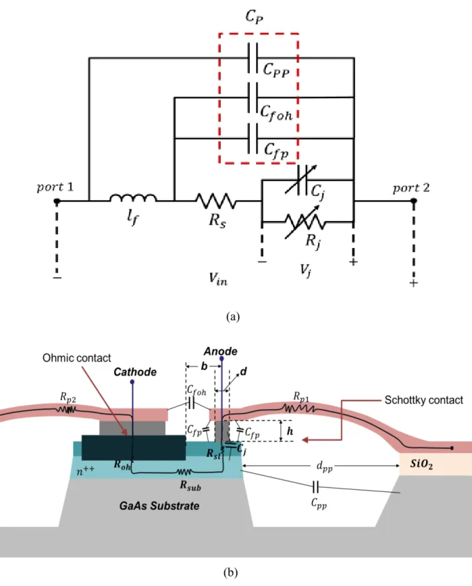
IX Figure 3-2. (a) Diode equivalent circuit model. 𝐶𝑝𝑝 is the pad-to-pad parasitic capacitance, 𝐶𝑓𝑝 is the capacitance between finger and mesa, and 𝐶𝑓𝑜ℎ is the capacitance between finger and the Ohmic contact; (b) Schematic of diode side view and equivalent circuit components. Parasitics 𝑅𝑝1, 𝑅𝑝2, 𝑅𝑜ℎ, 𝑅𝑠𝑢𝑏 and 𝑅𝑠𝑙 are anode finger, Ohmic air-bridge, Ohmic contact, n-well doped channel and the un-depleted Schottky layer resistance, respectively. ... 26 Figure 3-3. Ratio of the absorbed power in the junction resistance Rj to the total absorbed RF power. The maximum ratio value at each bias point occurrs at ω = 0 and is equal to Rj(Rs + Rj). The cut-off frequency is defined as the frequency for which this ratio reduces to half of the maximum value. ... 29 Figure 3-4. Junction resistance power ratio 𝑃𝑅𝑗𝑃𝑅𝐹 as a function of voltage bias and frequency. ... 30 Figure 3-5. Comparison between different methods for cut-off frequency calculation. The 𝑓𝐶 is the second approach and 𝑓𝐶𝑟𝑗 is the third approach (mixer and multiplier applications). The 𝑓𝑅𝑗 is the fourth approach, for direct detection applications. ... 32 Figure 3-6. Cut-off frequency of diode for direct detection/ rectification applications (it is assumed that the circular diode contact has 1 µm radius). 𝑓𝑅𝑗 is calculated by Eq. (2) and 𝑓𝑃𝑟𝑗 is the new approach with 10, 20, and 40 percent minimum efficiency of absorbed power in 𝑅𝑗. The results are presented for two channel thicknesses of less than 350 nm and 1.2 μm. In the cut-off calculation the impact of parasitic capacitance of diode is taken into account by using CT=Cj+Cp. ... 34
Figure 3-7. The simulation result of rectified current for 1 µm anode radius of this work design when the input signal amplitude is 5 mV. ... 35 Figure 3-8. The estimated current responsivity βi1 as a function bias voltage for 300, 600 and 1000 GHz. ... 37 Figure 3-9. The estimated voltage responsivity βv1, as a function bias voltage for 300, 600 and 1000 GHz. ... 38 Figure 3-10. The frequency independent part of Noise Equivalent Power (NEP)0 as a function of
X Figure 3-11. Noise Equivalent Power (NEP) as a function of frequency for the designed diode with 1 µm anode radius at 0.82 V voltage bias. ... 39 Figure 4-1. Cut-off frequency of a diode for direct detection applications as a function of the Schottky layer thickness for different voltage biases. The diode has a 1 µm radius circular anode contact and a 4× 10¹⁶ 𝑐𝑚 − 3 doped Schottky layer and channel thickness D=1.2 μm. The results are compered at Vb=0.85 V with 𝑓𝑅𝑗 (Eq. 2) and the new approach for channel thickness (D) <350
nm (as it is in the fabricated diode in this work)... 44 Figure 4-2. The multiplier application cut-off frequency of the diode, with 1 µm radius circular anode contact and 4× 10¹⁶𝑐𝑚 − 3 doped Schottky layer, as a function of Schottky layer thickness for different bias points. The results are compared for two channel thickness (D) <350 nm (as it is in the fabricated diode in this work) and 1.2 μm. In the cut-off calculation the impact of parasitic capacitance of diode is taken into account by using CT=Cj+Cp. ... 45
Figure 4-3 The designed structures and diodes on the mask, (a) the single diodes configuration for CD measurement, (b) the series configuration of the single diode for two probe RF measurement, (c) the shunt configuration of the single diode for one probe RF measurement, (d) the RTL on-board calibration kit. ... 49 Figure 4-4 Schematic explanation of the diode primary fabrication process. ... 53 Figure 4-5 SEM image of the fabricated diode by the Multi-SM process, (a) The diode view, (b) Anode finger zoom in. ... 54 Figure 4-6. Trench filled by coating several layer of PMMA and covered by thick photoresist. The green lines illustrate the multiple layers of PMMA gradually filling and partially planarizing the trench... 56 Figure 4-7. Planarization process: trench filled by coating several layer of PMMA and cover resist is patterned to remain just over the trenches. The resist surface transforms during the etching back process... 58
XI Figure 4-8 The planarization etch-back stop point: (a) The Multi-SM process etch stop point effect on the diode structure, (b) The Double-SM process etch stop point effect is vanished by using a second resist (PMGI) on the planarized PMMA to support the air bridges. ... 59 Figure 4-9. Three layers resist process to make a T-shaped contact bridge. ... 61 Figure 4-10 SEM images of diodes fabricated with the double-SM method. a) Global view of the mesa, Schottky and Ohmic contacts. b) Anode region with the stand-off height indicated. ... 62 Figure 4-11 The ohmic contact annealing issue, The contact metals 𝑁𝑖/𝐺𝑒/𝐴𝑢/𝑁𝑖/𝐴𝑢 are thermally evaporated, (a) before annealing (b) after annealing. ... 63 Figure 4-12 The modified ohmic contact after annealing. The contact metals 𝐺𝑒/𝐴𝑢/𝑁𝑖/𝐴𝑢 are thermally evaporated. ... 64 Figure 4-13 The wet etching process of the trenches. ... 65 Figure 4-14 Spreading of PMMA over a trench (a) One thick layer that get extreme tension at the trench edges, (b) The multi layers start from thin to thicker layers. ... 67 Figure 4-15 A cross section surface profile of the diode, when the trenches are filled by PMMA. ... 68 Figure 4-16 Optical microscope image of the test sample that planarized without patterning the cover SHIPLEY. The PMMA around the motifs (trenches) is cleaned by Plasma Oxygen etching, but there is left over PMMA on the flat areas. ... 69 Figure 4-17. The stubborn resist walls at the edges of the resist pattern. ... 70 Figure 4-18. The diode cross section surface profile, measured by Dektak profilometer. (a) the empty trenches, (b) filled by PMMA, covered by SHPLEY 1818 and patterned (ready for etch-back), (c)in the half way of the etch-back process, and (d) after completed etch-back. ... 72 Figure 4-19. The SEM image of the sample that in the T-shape contact and air-bridge process, the LOR resist is used as the middle resist layer to provide the undercut. ... 74 Figure 5-1. Four probe I-V measurement setup. ... 77
XII Figure 5-2. The extraction of the saturation current from the measured I-V curve. ... 78 Figure 5-3. The extracted ideality factor from the measured current of the fabricated diode by using Eq. (5-2). ... 79 Figure 5-4 The junction resistance 𝑅𝑗 of the fabricated diode extracted from measured I-V curve. ... 80 Figure 5-5 Measured I-V curve of a 2 µm radius anode diode and the series resistance extraction from the slope of the curve at its high current regime which is almost resistive. ... 81 Figure 5-6 The current deviation method for extraction of the diode series resistance 𝑅𝑠. ... 82 Figure 5-7 The diagram of voltage delta ∆𝑉 as function of measured current for the fabricated diode with 2 µm radius anode. ... 83 Figure 5-8. Measured and simulated I-V curve of 2 µm radius circular anode diodes. ... 84 Figure 5-9. Equivalent circuit model components for 1µm anode radius diode. The junction and series resistance, 𝑅𝑗 and 𝑅𝑠, simulated and measured results. The measured 𝑅𝑠 at 0.9 V bias is ~48 Ω as it is marked by red cross sign. ... 85 Figure 5-10 The TLM structure that is used in this work. ... 86 Figure 5-11 Schematic of the TLM measurement results plotting and explanation of parameters extraction from the plot. ... 87 Figure 5-12 The side view of current flow between an ohmic contact and (a) a backside contact, (b) another contact in planar structure. ... 87 Figure 5-13 RF measurement setup. ... 89 Figure 5-14 The equivalent circuit of the diode + CPW lines that is simulated by ADS to fit the S-parameters with the measurement result and extract the diode capacitance. ... 89 Figure 5-15. The measured S21 parameter for a 1 µm anode radius diode and the fitted ADS model. The diode is in series between the two VNA ports. ... 90
XIII Figure 5-16. The measured and simulated total capacitance 𝐶𝑇 at zero bias for the diodes with anode radius between 0.8 to 2 µm. ... 91 Figure 5-17. The measured S21 parameter of the 1.25 µm radius diode at various voltage biases. The diode is in series between the two VNA ports. ... 92 Figure 5-18. Total capacitance 𝐶𝑇 that was extracted from measured S-parameters of the biased diodes from 0 V to 1 V and with (a) 1 µm, (b) 1.25 µm, (c) 1.5 µm and (d) 2 µm anode radius, is compared with the simulation results. ... 94 Figure 5-19 The back-to-back diodes structure with the connection onboard transmission line and measurement setup. ... 97 Figure 5-20 The back-to-back diodes multiplication measurement result for 6 GHz input signal with +14 dBm power. ... 98 Figure A-8-1 Metal and n-type semiconductor energy band diagrams, (a) before instance of contact, and (b) after contact is built, at thermal equilibrium. ... 104 Figure A-8-2 Metal-Semiconductor contact types energy band diagrams. Rectifying contacts: (a)Ф𝑚 > Ф𝑠 for an n-type semiconductor (a1) before joining (a2) the junction equilibrium energy diagram, (b)Ф𝑚 < Ф𝑠 for an p-type semiconductor (b1) before joining (b2) the junction equilibrium energy diagram. Ohmic contact: (c) Ф𝑚 < Ф𝑠 for an n-type semiconductor (c1) before joining (c2) the junction equilibrium energy diagram, (d) Ф𝑚 > Ф𝑠 for an p-type semiconductor (d1) before joining (d2) the junction equilibrium energy diagram [93]. ... 107 Figure A-8-3 Energy diagram of the practical Schottky diode in forward, zero and reverse biases. qΔФ is the Schottky effect reduction of barrier height due to the thermal equilibrium. ... 109 Figure A-8-4 The Schottky contact energy diagram in forward, zero and reverse biases. ... 109
1
1 Introduction
1.1 Terahertz gap
Terahertz (THz) is an electromagnetic spectrum that lies between microwave and infrared frequencies. This frequency band does not have unique definition. However, many references are considering it as the spectrum between100 GHz (0.1 THz) and 30 THz. A variety of novel applications have been introduced within this spectrum, inspired by optical and microwave technologies, and advances in micro- and nano-fabrication techniques, [1].
Due to existence of molecular resonances and other physical phenomena in THz band, many applications can leverage such properties. At the same time, it is the least explored part of the spectrum (hence a so-called “THz gap” [2]), due to the lack of efficient active and passive components. More precisely, there is currently no low-cost, compact and efficient sources and detectors [3], [4]. Nevertheless, thanks to the enormous research efforts, performed during the past decades, the size of the gap has been diminished. The first practical solution for using THz band was generating and detecting of pulsed THz waves by femtosecond-pulse lasers in the early 1990s [5]. Later in the 2000s by development of THz semiconductor devices a new chapter in this technology has been opened and fueled many interesting applications.
1.2 Terahertz applications
The THz range became a hot topic during the past decades due to several interesting potential applications, such as a high data rate short-range communication, spectroscopy, biology (disease detection, e.g. cancer), astronomy, imaging, security, terrain mapping, and environmental studies [6].
Spectroscopy is one of the main applications of THz waves because of the spectral signature molecules, especially the organics and biologicals, in this region. THz radiation can transmit through opaque materials while it excites their molecular resonance and it is sensitive to bonding of atoms. Materials can be categorized into three categories according to their behaviors when they are exposed to THz radiation. Metals are highly reflective, polar materials (water) are highly
2 absorptive, and nonpolar and nonmetallic material such as plastic, wood, paper, and fabrics which are opaque to the optical frequencies, are transparent to the THz frequencies [2]. This make this region of spectrum ideal for imaging applications. Figure 1-1 shows an integrated circuit (IC) image with visible light and THz imaging. The metal circuit and the semiconductor wafer inside the IC package are visible to THz waves [4]. Moreover, the THz gap is a free frequency band for high data rate communications. The demand for bandwidth in wireless communications has doubled every 18 months for the past 25 years [7]. Thus, moving to higher frequencies to have wider bandwidth is inevitable. A fully integrated THz system can facilitate the path toward the next generation of telecommunication systems.
Figure 1-1 Image of an IC using (a) visible light and (b) with THz imaging. The IC black epoxy package [4].
1.3 Terahertz devices
THz circuits consists of different active (e.g. diodes and transistors) and passive (e.g. waveguides, antennas, and filters) elements. Many researches have been dedicated to provide a compact, efficient and low-cost materials and solutions to overcome the lack of THz components. For instance, considering waveguides, various structures made of either metallic or dielectric materials have been proposed in the literature [8]–[10]. Metallic waveguides suffer from metallic losses of metal parts while dielectric waveguides suffer from radiation and dielectric losses. Although planar structures are more lossy, they are more attractive since they are able to be integrated with other active components.
(a)
3 THz detection and generation is the most important and challenging part of THz systems. Detectors and sources could come from microwave-electronic devices, optical approaches or a combination of both [11]. However, for the THz region, RF detectors demonstrated superior performance compared to their optical counterparts [12]. THz detectors can be divided into incoherent (direct) and coherent (mixing) categories [13]. A simple schematic of both direct and mixing detection approaches is shown in Figure 1-2. Bolometers and pyroelectric crystals fall into the direct category, however, they are slow and perform only in low temperatures. Coherent detectors include nonlinear optical crystals, photoconductive antennas [14], hot electron bolometers (HEBs), superconducting tunnel junctions (STJs), superconductor-isolator-superconductor (SIS) tunnel junctions, tunneling quantum dot inter-sublevel photo-detectors (T-QDIPs), and Schottky diodes. STJs, SISs, HEBs, and T-QDIPs are cryogenic detectors while the others can function on room temperature.
A bolometer is a thermal detector that includes a temperature-dependent resistance and two metallic contacts. The resistive element is made of a very low thermal capacity and high temperature coefficient material that can provide a large resistance variation according to the input signal [3]. High mobility semiconductors with temperature sensitivity or superconductor can be used for THz bolometers at cryogenic temperatures.
The high electron mobility transistors (HEMTs) lately become very interesting in THz region especially for detection and generation. These structures naturally promoting emission and detection of THz waves, due to its two-dimensional (2D) Plasmon in hetero-structure semiconductor that provide a channel with high mobility and low resistivity [15]–[22].
Between all technologies used for THz detection and generation, the suitable technology should be chosen base on project requirements, application, budget, and available fabrication facilities. Some of the noted technologies are cryogenic and require a low temperature system; others are limited by the size of the device or designed just for pulse operation. Schottky diodes are compatible with pulsed and continuous signals and can operate at room temperature. The GaAs Schottky diode provides high sensitivity, large instantaneous bandwidth, and large spectral resolution [23]. Hence, Schottky diode technology was selected for this thesis.
4
(a) (b)
Figure 1-2 Schematic of different detector types. (a) Direct detection. (b) Mixing detection.
1.4 Schottky diode for THz applications
The Schottky diodes have been employed in different application in THz systems (e.g. sources, detectors, mixers, and phase-shifters) [24]–[27]. Different properties of diodes are leveraged according to the application that they are used for. In detection systems, diodes are used as a rectifier (direct detection) where the nonlinear resistive element of diode and its current value are the key elements. However, in the heterodyne detectors and sources where the diode is used as a mixer and multiplier, the key element is the diode nonlinear capacitance. Therefore, the diode application should be considered in design and performance study. Moreover, at design stage, considering application will result in better optimization of the diode. So far, several research dedicated to study the diodes in terms of equivalent circuit, design, structure, fabrication, frequency performance, efficiency, temperature noise, and parasitic effects [28]–[35]. Nevertheless, the application based study of the diode and its effect on the design and optimization is missed. In this work, an application based studies of diode and comparison of its performance in different applications is reported. The design and optimization of the diode by considering its application are proposed. Also, comprehensive studies of the diode frequency behavior for each application categories are presented. The diode frequency behavior is characterized by the cut-off frequency, which is defined by the power portion of the used nonlinear element of the diode. Since, in each category the used nonlinear element is different, the cut-off frequency and its formulation
5 should be defined based on the application. In the presented cut-off frequencies formulation, the effect of all circuit elements of the diode is considered.
In this thesis, a THz Schottky diode is developed to be used in integrated circuits operating at room temperature and able to work with pulse or continuous signals. The developed diode in this work has a lower parasitic capacitance that improves the cut-off frequency. Also, the lack of effective fabrication process for the diode mass production encouraged us to develop a low-cost, reliable, repeatable and flexible fabrication process. GaAs is selected as the semiconductor host because it has high sensitivity, large bandwidth, and spectral resolution. GaAs is one of the best choices among the semiconductors for the THz frequency, due to the high saturated electron velocity and electron mobility. It has lower parasitic resistivity and lower noise. Moreover, GaAs devices are less sensitive to own heating due to their wide energy band-gap. On the other hand pure GaAs has high resistivity and high dielectric constant which provides very good isolation when it is used as a substrate at high frequencies.
1.5 Thesis outline
This thesis includes six chapters. In Chapter 2, the Schottky diode definition, structure, history, applications in THz frequencies, and the state of the art are discussed. The design process, simulation, and analytical studies of the diode are presented in chapter 3. Also in chapter 3, different approaches for studying the diode performance are discussed and a new, more accurate approach is suggested. The epitaxy structure engineering for the diode which depends on the diode application and the unique fabrication process that is developed for realization of the diodes is described in chapter 4. Moreover, the mask design, details of the fabrication process and challenges faced during the process development are described in chapter 4. In chapter 5, the characterization and measurement results, setups, procedures, and parameter extraction methods used for the characterization of diode are explained. The conclusion of this work and some suggestions for further research are provided in chapter 6.
6
2 Literature Review: Toward THz
Schottky Diode
2.1 Introduction
In order to achieve practical THz systems at room temperature with reasonable size and cost to meet various application requirements, a versatile, flexible and compact integrated transceiver system is required [36]. The Schottky diode is one of the most useful and popular device for millimetre-wave and THz detection. The planar structure of the diode is very compact, integrable, mechanically stable, and low noise [37]. Therefore, the Schottky diode can be an essential and critical element of THz systems. The diode is based on the metal-semiconductor rectifying system. For the first time, in 1938, Walter Schottky presented a theory that, expresses the capability of raising potential across the semiconductor’s barrier, is so-called the Schottky barrier. Meantime, Mott presented another theoretical model for potential across the metal-semiconductor junction which is called the Mott operation [38]. Appendix A presents an overview of Schottky and metal-semiconductor contacts.
2.2 Schottky diode
A Schottky diode is a metal-semiconductor contact in which the work function of the metal is higher than that of the semiconductor (𝜙𝑚 > 𝜙𝑠). In order for the device to be able to pass the
current, it needs another connection as second port. Therefore, another metal-semiconductor contact but in Ohmic mode (Appendix A) is required. The device structure is shown in Figure 2-1.
7 Figure 2-1 The Schottky diode structure.
A general explanation of the metal-semiconductor contacts is given in Appendix A. The heart of the diode is a Schottky mode metal-semiconductor contact. The interface of the semiconductor with metal is depleted due to the difference of the work functions. The depletion region width 𝑊𝐷
depends on the junction build-in potential 𝜑𝑏𝑖, the Schottky layer doping level 𝑁𝐷, its permittivity
𝜀𝑠, and the junction voltage bias 𝑉𝑗;
The junction capacitance 𝐶𝑗 of this contact is a function of the depletion region width 𝑊𝐷:
where A is the junction area. Therefore, the junction capacitance is a function of voltage bias. Since the main current transport mechanism of the Schottky diode is thermionic emission, when the positive voltage bias is applied (forward bias regime) the diode current is obtained by:
𝑊𝐷(𝑉𝑗) = √2 𝜀𝑠
𝑞 𝑁𝐷(𝜑𝑏𝑖− 𝑉𝑗) (2-1)
𝐶𝑗(𝑉𝑗) = 𝐴 𝜀𝑠
8 where 𝑘𝐵 is Boltzmann’s constant, T is the temperature, and 𝐼𝑠 is saturation current. That is:
where 𝑅∗ is Richardson’s constant. Since the diode also includes a series resistance 𝑅
𝑠 due to the
resistivity of contacts and the current path though the semiconductor (here GaAs), the applied voltage bias 𝑉𝑏 and the junction voltage 𝑉𝑗 relation is expressed as:
In this work we developed an analytical model of Schottky diode based on expanded physical behavior analysis as briefly explained above. The diode behavior is simulated and studied by using this developed simulation environment to optimize and characterize the diode barrier, equivalent circuit, and parasitic elements.
In order to develop the Schottky diode for THz applications some improvement (mainly in design process) are required. Modifications such as; using a high mobility semiconductor host, reducing the capacitance of the diode by reducing its anode size, minimizing the parasitic elements, and reducing the system noise.
2.3 Development of the diode structure and
technologies
THz Schottky diodes are presented in different configuration such as whisker contact, planar (with surface channels), quasi-vertical (anode and cathode are vertically mounted and has surface channel interconnection), and two dimensional electron gas Schottky layer structure.
𝐼 = 𝐼𝑠(exp ( 𝑞 𝑉𝑗 𝑘𝐵𝑇 ) − 1) (2-3) 𝐼𝑠 = 𝐴 𝑅∗𝑇2 exp (− 𝑞 𝜑𝐵 𝑘𝐵𝑇 ) (2-4) 𝑉𝑗 = 𝑉𝑏− 𝐼 𝑅𝑠 (2-5)
9
2.3.1 Whisker diode
Young and Irvin (1965) proposed the first technique that is used for realization of sub-millimeter (sub-mm) waves and THz Schottky diodes, called a “whisker diode.” The technique was based on gently squeezing off a metallic whisker on GaAs epitaxy die which had a large Ohmic contact on the back side of the chip [39]. At the end of 1980 decade, T. Crowe and colleagues at the University of Virginia started working on sub-mm and THz systems based on GaAs Schottky diodes [40]. They have used Young and Irvin’s fabrication technology of vertical structure diodes [39]. A cross-sectional view of this diode is shown in Figure 2-2. In order to couple to this diode, they used whisker contact to minimize the diode’s additional coupling series resistance and shunt capacitance. The diode with the whisker contact is shown in Figure 2-3. After Young and Irvin,
many research teams at the University of Virginia, Bell Labs, MIT, Chalmers, and Texas Instruments tried to improve and optimize design and fabrication technology
of epitaxial GaAs Schottky diodes. They studied the effect of electron tunneling across the barrier of the diode current-voltage (I-V) curve [41]. Also, they investigated the diode series resistance behavior as a function of skin effect and plasma resonance [42]. Another researcher studied the source of the noises, such as hot-electron noise, in the diode [43].
10 Figure 2-3 SEM image of vertical structure Schottky diode with Whisker contact [44].
2.3.2 Planar structures
In parallel with THz whisker diode development, improvement in micro-fabrication methods and technology enabled reaching new frontiers by:
- reducing the size of the Anode
- controlling doping concentration and thickness of each layer of the epitaxy structure - air-bridge techniques to reduce the parasitic elements
which improved the diode performance and increased its cut-off frequency. Then, W. Bishop et al. (1990) presented the first planar Schottky diode which has attracted much attention [37]. This planar diode was realized by making both contacts on one side of the chip, and employing bridges to connect the anode and cathode to the circuit. Figure 2-4 shows the schematic side view of the proposed diode in [37].The planar structure can work at THz frequencies by using air bridges, which have lower parasitic capacitance. The planar diode is preferred over the whisker design due to its compactness, ease of integration, and mechanical stability. However, due to the whisker diode’s vertical structure, the anode placed directly over the backside Ohmic contact has smaller parasitic capacitance and series resistance in comparison to planar structures. The advancement from whisker to a planar device gives freedom to develop integrated circuits based on Schottky
11 diodes suitable for many applications [27], [45]–[47]. The planar diodes have been realized with different materials and technologies such as CMOS [48], GaAs, and GaN [49]. Epitaxial GaAs Schottky barrier diodes are frequently used in THz heterodyne detectors, mixers, and solid state sources. After the introduction of the planar diodes in [13], many researches focused on improving the diode performances in terms of cut-off frequency, efficiency, responsivity, sensitivity, and device noises. Also, RF losses and thermal heating are discussed in the literature [11], [35]. In [11] the electro-thermal model of the Schottky diode is presented. This model can give the device hot spot temperatures which will be helpful for circuit reliability studies.
Figure 2-4 Schematic of cross section view of surface channel diode [37]
2.3.3 Quasi-vertical structures
The quasi-vertical is another reported structure, which is combination of the two above structures [50]–[53]. In this structure, the anode and cathode are placed vertically while the structure is planar. The quasi-vertical diode is achieved by making a large ohmic contact (cathode) from the back side below the anode contact while both anode and cathode have access from top side, as shown in Figure 2-5. This structure is easier to integrate than the whisker structure due to surface channel anode access, and also has vertical structure advantages. However, the vertical structure diode has some limitation due to its backside process requirement which add some complexity to the fabrication process.
12 A quasi-vertical Schottky diode [50] has recently been reported that can be integrated into planar millimeter and submillimeter-wave circuits. The diode structure is based on backside processing and bonding of the diode epitaxy to a host high-resistivity silicon substrate that supports both the vertical diode and its associated circuitry (Figure 2-5).
Figure 2-5 Schematic of quasi-vertical diode [50].
2.3.4 2D electron gas Schottky diode
In 1992, W. Peatman at Virginia University proposed a new two-dimensional electron gas (2DEG) based millimeter/sub-millimeter diode for multiplication applications [54]. The Schottky contact was placed along the edge of a 2DEG based on AlGaAs/InGaAs/GaAs heterostructure (geometry of the structure is shown in Figure 2-6). This geometry has the combination of low series resistance and high breakdown voltage. The high breakdown caused by the 2D electric field spreading in the depletion region and the low series resistance is due to the excellent transport properties of the 2DEG. Meanwhile, the electron transit-time of this structure is lower than the conventional Schottky diode due to high electron velocity of the 2DEG. Also, a 2DEG Schottky diode by AlGaN/GaN heterostructure for THz detection is experimentally demonstrated in [49].
13
2.3.5 CMOS technology diode
CMOS technology was also used for realization of the Schottky diode for high frequency applications. The first mmWave Schottky diode frequency doubler fabricated in CMOS was presented in [48]. An array of the diodes shunt connected were implemented in CMOS technology without any process modifications. Due to the shunt array, the series resistance was reduced, which increased the cut-off frequency. In the fabrication of diodes, CoSi2 is used in the interface of
metal-semiconductor contact which enhanced the barrier height. The CoSi2-Si diodes on the n- and
p-well substrates are fabricated without a guard ring in 130-nm foundry CMOS process. By using these techniques, they reached the highest cut-off frequencies for Schottky diodes fabricated with silicon. This work shows the CMOS technology potential for mmWave and far-infrared detection systems. The idea was used in [55] for an 8x8 parallel Schottky diode in CMOS technology. The proposed diode in [48] was also used in sub-millimeter CMOS integrated circuits and presented in [56] and [57]. A broadband detector for 0.6 to 1 THz using 65 nm CMOS technology and integrated silicon lens for imaging is presented in [58].
14 According to this summary of the diode structures and technology, the diode has been realized in not integrable whisker contact or integrated planar structure although it sacrifices partly the diode performance due to the higher parasitic elements. However, by developing the micro/nano-fabrication techniques the parasitic problem has been significantly diminished. A mixed structure is called quasi-vertical is developed that has both structures benefits. Also, some other technologies such as 2D electron gas and CMOS are used in the diode design and realization.
2.4 THz Schottky diode applications
In previous sections, different THz Schottky diode technologies, which have been published in literature, are reviewed. In this thesis, in order to achieve better integration capability, planar structures are considered. Planar configuration are more attractive since they are well-developed for different applications. Also, in most performed researches and investigations, studies were not considering diode’s application. Therefore, this thesis is focused on bringing a comprehensive study and generalized design methodology for different diode applications. In the following subsections, multiple applications are discussed and comprehensive literature review is performed.
2.4.1 Mixer diode-heterodyne receiver
In [31], the planar diode, which was presented by the University of Virginia research team [37], is used around 800 GHz and it is shown in Figure 2-7 (a). Also, back-to-back diodes were presented as a mixer in a heterodyne receiver (see Figure 2-7 (b)). They studied the thermal noise and sources of the losses in the diode circuit. In this kind of receiver, diodes are the source of the noise, but most losses occur between the antenna and mixer. In another work [32], they studied physics of a diode with degenerately-doped GaAs and the effect of this heavily doped barrier for THz application of the device.
Meanwhile, the JPL (Jet Propulsion Laboratory) group proposed a monolithic mixer based on the Schottky diode, which achieved 2.5 THz frequency at room-temperature [59]. The diode and circuit membrane were based on a GaAs substrate. The mixer is employed in a heterodyne THz detection system. The received signal is mixed with a signal generated by far-infrared laser oscillator and provides an RF signal at few GHz. In the diode fabrication, they employed a T-shape anode technique presented by Alien and Reddy from the University of California, Santa Barbara
15 [60], [61]. A thin GaAs membrane was used to prevent the bulk substrate skin-depth effect, which increased the diode resistance at high frequency as discussed in [40]. Figure 2-8 is a SEM image of the 2.5 THz monolithic mixer with the GaAs membrane. This membrane was created by making a wide and deep trench all around and under the circuit strip.
(a) (b)
Figure 2-7 The Planar Schottky diode which presented by the Crowe team in 1991 [31].
(a) (b)
Figure 2-8 SEM image of (a) the 2.5 THz Monolithic Schottky diode mixer with the thin GaAs membrane, (b) the diode zoom in image [59].
16
2.4.2 Multiplier diode- THz source
Thereafter, a cryogenic all solid-state monolithic multiplier chain with 1.5 THz output signal is presented [46]. The multiplier chain provided the 1.5 THz signal by four steps doubling of a 95 GHz input signal with a membrane diodes arrays chain. The block diagram of the complete multiplier source containing a cascade of four frequency doublers is shown in Figure 2-9. The applied diodes in the chain are separately designed and fabricated for their frequency range. The diodes’ fabrication was described in two categories, one for the frequencies below 1 THz and second for the frequencies above 1 THz. For instance, photolithography is employed in the first group to make the anode contact. However, since a much smaller anode contact area (~0.3 𝜇𝑚2)
is required, in the second diodes group (over 1 THz), an electron-beam lithography process was used in the anode contact process. A summary of the THz sources based on GaAs Schottky diode multiplier is presented in [62].
Figure 2-9 Schematic block diagram of the all-solid-state 1500-GHz multiplier source by using four-step multiplier chain [46].
A substrate-less Schottky diode-based multiplier at 200, 400 and 800GHz was presented by the JPL group [63]. The design reduced RF losses and improved system efficiency. Figure 2-10 shows how the 400GHz substrate-less doubler with a GaAs frame holder implemented which is excited by input rectangular waveguide. Then, a Schottky diode tripler at 1.9 THz was presented by developing the previous technology in [64].
17 Figure 2-11 is the 3D view of the 1.9 THz GaAs Schottky diode-based tripler. It shows the configuration of diodes in the circuit and how the ciruit excites the input and output rectangular waveguides.
A continuous wave coherent source at room temperature for 2.5 THz is presented in [65]. This source with unprecedented 270 GHz bandwidth, achieved by using three cascaded Schottky diode-based frequency triplers, can be used in continuous wave, modulated or pulsed mode.
2.4.3 All-solid-state heterodyne receiver
A 1.2 THz receiver based on the Schottky diode mixer was presented in [66]. In this design, the mixer local oscillator (LO) signal was also provided by a Schottky diode-based multiplier chain [66]. It was the first all-solid-state heterodyne receiver in the 1.2 THz range which worked at room temperature. There was another diode-based mixing system with diode chain LO at 900 GHz presented in [67] that has a cryogenic system to cool the mixer to 120 K.
18
2.4.4 Rectifier diode- direct detection
In the high frequency bands, direct detection is very attractive since there is no need for local oscillator. To do so, Schottky diodes have been used for direct detection in THz band.
A broadband THz detector based on a zero-bias Schottky diode is introduced in [69]. The diode and on-chip lithographic antenna are bonded to a hemispherical silicon lens. Both the top and side views of this broadband THz detector are shown in Figure 2-12. The diode is mounted across the feed point of the sinuous antennas by using a flip-chip technique. In [25], a THz rectification system is presented which has the detector diode and the planar antenna fabricated together to improve performance by decreasing the diode size. Also, a tunable lens-coupled annular-slot antenna and a Schottky diode rectifier are reported in [70]. The resonance frequency of the slot antenna is tuned from 140 to 220 GHz by diode capacitance which is a bias dependent variable.
19 Figure 2-12 Broadband THz detector based on direct detection, (a) the planar sinuous antenna with a flip-chip diode in the center, (b) the diode detector and antenna mounted on a hemispherical silicon substrate lens [69].
In this chapter the diode structural progress, technologies and application developments in the literature are summarized. In most reported works the focus have been on the method of using the diode in a specific application and circuit. The diode itself, design, and optimization is studied in a limited number of reports such as [28], [29], [42], [71]. And the diode characterization is studied in [25], [33], [72], [73]. So, there is a lack of comprehensive study on the diode based on its application and comparison of its performance in each application. Also, studies of application impact on the diode design are missing in the literature. Therefore in this thesis, the diode optimization and frequency behavior based on the application are categorized and compared. On the other hand, the fabrication processes presented in the literature [25], [30], [46], [74], [75] are not cost-effective, flexible, reliable, and repeatable enough to use for mass production and commercial application of the diode. In this thesis, a fabrication process for the diode mass production is presented which is low-cost, more flexible, and easy to repeat is presented.
20
3 Schottky Diode Application-based
Study
Submillimeter Wave GaAs Schottky Diode
Application-Based Study and Optimization for 0.1- 1.5 THz
Here a design and optimization method for Schottky diodes is proposed. By employing the optimization method, parasitic capacitance of the diode is significantly reduced (under 20% of the total capacitance) to be able to operate up to 1.5 THz which is confirmed through DC and RF measurements presented in chapter 5. The diode responsivity and noise equivalent power (NEP) is also investigated. Moreover, limiting factors of the diode cut-off frequency in mixer/multiplier and detector mode applications are studied. It is shown that, in mixer/multiplier mode, the usable voltage bias range (with acceptable cut-off frequency) is limited by the exponential reduction of Rj. Therefore, a new approach for more practical cut-off frequency calculation is introduced which
is valid for wide ranges of Rj values. Also, a detailed formula is presented for calculation of the
diode cut-off frequency for the detector application mode.
3.1 Introduction
There is great interest in the submillimeter-wave spectrum due to its numerous applications in astronomy, spectroscopy, security, surveillance, disease detection, DNA identification and telecommunication [76], [77]. Lack of compact and efficient submillimeter-wave active and passive components slow down technological progress required for realization of the aforementioned applications. Neither design, simulation nor fabrication of these components are fully developed, with fabrication being the biggest challenge.
Diodes are critical elements in submillimeter-wave circuits. During recent decades, GaAs Schottky barrier diodes have been the preferred choice and have had the most significant progress. They are presently used in several submillimeter and terahertz (THz) circuits such as mixers [40], [45], [46], [59], multipliers in solid state sources [46], phase shifters [27], and detectors [25]. For instance, in
21 [46], an all solid-state monolithic multiplier chain of membrane diodes is presented where the multiplier chain employs four doubling steps to reach 1.5 THz from 95 GHz input signal. This Schottky diode-based multiplier was developed to serve as a submillimeter-wave local oscillator for a heterodyne receiver.
Cut-off frequency is the main parameter in defining the behavior of a diode. It is estimated by 𝑓𝑐 =
1 2𝜋𝐶⁄ 𝑗𝑅𝑠 where 𝑅𝑠 and 𝐶𝑗 are series resistance and junction capacitance respectively [38], [48].
However, influence of other components of the diode equivalent circuit model and their bias dependency needs to be considered to achieve more accurate results. It is also of significant importance to provide an application-based study for the diode cut-off frequency since different sources of nonlinearity is targeted.
In order to expand the diode cut-off frequency to submillimeter-wave region, reducing the junction capacitance by shrinking the anode size has been the main approach [31], [47], [63]. However, aside from the junction capacitance, the parasitic elements such as parasitic capacitance, have high impact on the diode frequency performance and limits the cut-off frequency. For instance, in [73] the reported parasitic capacitance is 4-5 times larger than the junction capacitance. Therefore, the diode performance is mainly limited by its parasitic elements rather than the junction capacitance. In the present work, we review and compare four approaches to estimating the cut-off frequency of Schottky diodes. In particular, we extend these approaches by considering the bias dependence of all components, and discuss new limitations that arise.
3.2 Design and Simulation
The design process starts by specifying the frequency range of operation. It is first necessary to define the electron mobility and plasma frequency. These parameters are used to select the appropriate semiconductor and its doping density. Then, based on the wafer specifications, i.e., layers architecture and their properties including thickness, dopant and electron mobility, the performance of the diode can be simulated. A set of design parameters are assumed as the initial values and further optimizations are performed to achieve the desired characteristics. The input variables are semiconductor active layers (Schottky and n-well doped layers) doping, mobility, resistivity and their thicknesses, contact
22 areas, shapes and their distance, both contact barrier heights, specific contact resistivity (Ohmic), operating frequency, and temperature.
The aforementioned calculations are accomplished by developing a code based on the analytical model of diode. The flowchart of the described design and optimization process is shown in Figure 3-1. Fabrication limitations, such as achievable UV-lithography alignment and precision and having access to high mobility GaAs epitaxy wafers should be taken into account. Initial value of some parameters may be extracted from literature at the beginning to estimate and optimize requirements of epitaxy structure. After determining the epitaxy structure, the parameters (such as contacts barrier heights, specific contact resistivity, layers resistivity and mobility) are replaced by measurement results from quick tests such as TLM, C-V and Van-der-Pauw.
23 Figure 3-1. Design and optimization process for Schottky diodes.
24
3.3 Optimization
The cut-off frequency of diodes and related operating frequency ranges are generally linked to the series resistance and junction capacitance through the 𝑅𝑠∙ 𝐶𝑗 factor. Therefore, most of the
literature focuses on decreasing the anode dimensions to reduce the junction capacitance, and thereby improve the cut-off frequency.
Figure 3-2 (a) shows the Schottky diode equivalent circuit. The diode parasitic components are identified for various parts of the device, as explained in Figure 3-2 (b). The total series resistance is 𝑅𝑠 = 𝑅𝑠𝑙(𝑉) + 𝑅𝑠𝑢𝑏+ 𝑅𝑜ℎ+ 𝑅𝑝1+ 𝑅𝑝2 in which only 𝑅𝑠𝑙 has dependency to voltage bias. 𝑅𝑠𝑙
represents the part of the Schottky layer that is not depleted and therefore grows sub-linearly with the voltage bias across the junction. The junction capacitance 𝐶𝑗 and the resistance 𝑅𝑗 are the heart
of the Schottky diode, which their voltage-dependency generates its nonlinear characteristic. The total capacitance is defined as 𝐶𝑇 = 𝐶𝑗(𝑉) + 𝐶𝑝 = 𝐶𝑗(𝑉) + 𝐶𝑓𝑝+ 𝐶𝑓𝑜ℎ+ 𝐶𝑝𝑝, where 𝐶𝑝 is the
sum of all parasitic capacitances. In this work, the impact of 𝐶𝑝 on the cut-off frequency is taken
into account by considering the total capacitance 𝐶𝑇 instead of 𝐶𝑗. Although 𝐶𝑝 and 𝐶𝑗, as shown
in Figure 3-2, are not exactly in parallel, 𝐶𝑇 gives a good estimation of the diode total capacitance
and practical cut-off frequency. By reducing the junction capacitance, 𝐶𝑇 is dominated by parasitic
term that becomes the main limitation of the device. In many cases the parasitic capacitance is shown to be several times larger than the junction 𝐶𝑗 itself. For example, in [78], diodes with anode
areas of ~1 μm2 have a total capacitance (𝐶
𝑇) of ~10 fF where the 𝐶𝑗 portion is only 1.5-2 fF. Also,
in [73] diodes with a claimed cut-off frequency of ~20 THz have 𝐶𝑗0=1.3-1.8 fF (𝐶𝑗 at zero bias)
and 𝐶𝑝= 5.5-8.5 fF. Therefore, practical cut-off frequencies for those diodes are in the range of
3.9-3.4 THz.
In this work, all parasitic capacitances are taken into account to accurately estimate the practically achievable cut-off frequency. A fabrication process is presented that decreases all parasitic capacitances. Therefore, for a given anode area, the total capacitance of the diode is smaller which leads to higher cut-off frequency. This is accomplished by:
25 Increasing the gap between the mesa surface and the finger (h in Figure 3-2 (b)) which
reduces the parasitic capacitance between finger and mesa (𝐶𝑓𝑝).
Increasing the distance between the anode finger and the Ohmic contact and its air-bridge. This reduces the parasitic capacitance between the finger and the Ohmic contact (𝐶𝑓𝑜ℎ).
Increasing the distance between the mesa and input/output transmission lines (here 15-20 μm). Also, embeding a trench (as deep as 5-8 μm) around the mesa to deliver a lower pad-to-pad parasitic capacitance 𝐶𝑝𝑝.
The Schottky layer also is of prime importance in optimizing the diode performance. In order to minimize 𝑅𝑠𝑙, the thickness and doping of the Schottky layer should be chosen so that it is fully
depleted at a bias voltage (𝑉𝑀𝑜𝑡𝑡) just below the desired operating bias. Below 𝑉𝑀𝑜𝑡𝑡 the diode
operates in the Mott condition [71], [79] and has a quasi-constant capacitance value, providing low non-linear component. At the operating bias, almost all the Schottky layer is depleted, thus minimizing 𝑅𝑠𝑙, and the capacitance 𝐶𝑗 varies with bias and can provide the required non-linear
behavior. These conditions are achieved for Schottky layer thicknesses between 70-130 nm, doping levels between 1016 to 1018, and by managing the diode operating bias to put the diode in
the optimal situation. Using a thin epilayer around 100 nm and less improves the drift velocity and effective scattering frequency of the Schottky layer [40]. By further increasing the voltage bias above 𝑉𝑀𝑜𝑡𝑡, both 𝐶𝑗 and 𝑅𝑠 start to increase and this reduces the cut-off frequency.
26 (a)
(b)
Figure 3-2. (a) Diode equivalent circuit model. 𝐶𝑝𝑝 is the pad-to-pad parasitic capacitance, 𝐶𝑓𝑝 is
the capacitance between finger and mesa, and 𝐶𝑓𝑜ℎ is the capacitance between finger and the
Ohmic contact; (b) Schematic of diode side view and equivalent circuit components. Parasitics 𝑅𝑝1, 𝑅𝑝2, 𝑅𝑜ℎ, 𝑅𝑠𝑢𝑏 and 𝑅𝑠𝑙 are anode finger, Ohmic air-bridge, Ohmic contact, n-well doped
27
3.4 Cut-off Frequency
In this section, five approaches to calculate the cut-off frequency are discussed. The first three apply to mixers and multipliers that usually make use of the diode capacitance which is the dominant non-linear term at low forward or reverse bias. The fourth and fifth approaches are mainly used in direct detection and rectification through the diode’s non-linear resistance which is more dominant in higher forward bias regime. The third approach is developed and improved for more accuracy by considering a detailed model and dependency of its components to the voltage bias for mixer/multipliers applications. Also, the fifth approach is developed that gives better understanding of the diode performance.
Approach 1:
In reverse or at low forward biases at radio frequencies, where the junction resistance 𝑅𝑗 is much
larger than junction reactance (𝑋𝑗 = 1 𝑗𝜔𝐶⁄ 𝑗), the equivalent circuit of Figure 3-2 (a) can be
simplified to a series RC circuit (𝑅𝑠 , 𝐶𝑗). Eq. (3-1) is the most common formula to calculate the
cut-off frequency of a diode.
where 𝑅𝑠 = 𝑅𝑠0and 𝐶𝑗 = 𝐶𝑗0 are the series resistance and the junction capacitance of diode at zero
bias, respectively.
Approach 2:
The bias voltage dependency of the diode’s parameters was not considered in approach 1. Therefore, in the second approach, Eq. (3-1) is applied while considering the bias dependence of the series resistance (𝑅𝑠) and the junction capacitance (𝐶𝑗). In the first and second approaches, the
frequency at which, the power wasted in 𝑅𝑠 is equal to half of the input power, is defined as the
cut-off frequency.
𝑓𝐶 = 1
28
Approach 3:
In the forward regime, the junction resistance 𝑅𝑗 decreases and becomes comparable to the junction
reactance 𝑋𝑗 and cannot be ignored. Here, all bias voltage dependences, the junction resistance
(𝑅𝑗) and the effect of parasitic capacitances are considered in the calculation of the cut-off
frequency.
In this approach the cut-off frequency definition is the same as in the second approach, where the parasitic series resistance absorbs half of the input power or:
𝑃𝑗 𝑃𝑖𝑛~ |𝑉𝑗|2 |𝑉𝑖𝑛|2 = 𝑅𝑗2+ (𝜔𝐶𝑇𝑅𝑗2)2 (𝑅𝑠(1 + (𝜔𝐶𝑇𝑅𝑗2)2) + 𝑅𝑗)2+ (𝜔𝐶𝑇𝑅𝑗2)2 =1 2 𝑦𝑖𝑒𝑙𝑑𝑠 → 𝑓𝐶𝑟𝑗 (3-2)
where the junction resistance at forward bias (𝑅𝑗) is given by:
𝑅𝑗 = 1
(𝜕𝐼 𝜕𝑉⁄ 𝑗) ≡ 1
𝐺 (3-3)
In this last equation 𝑉𝑗 is the voltage over the junction and is related to the forward bias voltage
(𝑉𝐹) as:
𝑉𝑗 = 𝑉𝐹− 𝐼𝑅𝑠 (3-4)
Approach 4:
For direct detection and rectification applications, the non-linear junction resistance is the only element of the diode equivalent circuit that plays role. Here, the absorbed power in junction resistance 𝑅𝑗 is the key parameter to define the cut-off frequency. It is defined as the frequency for
which the absorbed power in 𝑅𝑗 is reduced to half of its maximum value [80]. Eq. (3-5) gives the
29 𝑃𝑅𝑗 𝑃𝑅𝐹 = 𝑅𝑗 𝑅𝑠(1 + 𝜔2𝐶 𝑇2𝑅𝑗2) + 𝑅𝑗 (3-5)
Figure 3-3. Ratio of the absorbed power in the junction resistance Rj to the total absorbed RF
power. The maximum ratio value at each bias point occurrs at ω = 0 and is equal to Rj⁄(Rs+ Rj).
The cut-off frequency is defined as the frequency for which this ratio reduces to half of the maximum value.
In the fourth approach, the effect of parasitic capacitances through the total capacitance (𝐶𝑇)
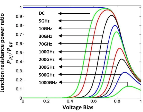
approximation, is considered like the third approach. Figure 3-3 shows the power ratio of Eq. (3-5) as a function of frequency for a fixed voltage bias (+0.83 V) for our diode with 1 µm anode radius (𝑟𝑎=1 µm). The cut-off frequency is extracted by that procedure for each bias value:
30 𝑓𝑅𝑗 = (1 +𝑅𝑅𝑠 𝑗) 1 2 ⁄ 2𝜋𝐶𝑇(𝑅𝑠𝑅𝑗)1⁄2 (3-6)
Figure 3-4. Junction resistance power ratio 𝑃𝑅𝑗⁄𝑃𝑅𝐹 as a function of voltage bias and frequency.
The maximum value for the absorbed power ratio in the junction resistance 𝑅𝑗, which happens at
DC, is shown in Figure 3-4 (DC labeled). This max-ratio starts to decrease at higher biases where 𝑅𝑗 is reduced enough to be comparable with the series resistance 𝑅𝑠. Also, the junction resistance power ratio 𝑃𝑅𝑗⁄𝑃𝑅𝐹 is shown in Figure 3-4 as a function of the bias voltage changes for
frequencies going from DC to 1 THz. For each frequency, the peak power ratio occurs at a bias voltage for which 𝑅𝑗 and 𝐶𝑇 reactance (𝑋𝐶𝑇) are in balance (𝑋𝐶𝑇 = √Rj(Rj||Rs)). As the frequency
31 increases, the decrease of the maximum power absorbed in 𝑅𝑗 is indicative of the reduction of the
detection/rectification efficiency. Using half of the total power definition for the cut-off frequency, that has been used in the previous approaches, would result in limiting the diode below ~100 GHz despite the fact that the diode can still function above that frequency, but with a reduced efficiency as will be shown in section section 3.5.
The four approaches are illustrated in Figure 3-5at forward biases for the 1 μm anode radius diode. The cut-off frequency reduction of the third approach (𝑓𝐶𝑟𝑗) with respect to the second approach
(𝑓𝐶) comes from the parasitic capacitances (𝐶𝑝) impact. The behavior difference in higher voltage
range is due to the rapidly decreasing 𝑅𝑗 with bias. This 𝑅𝑗 reduction dramatically reduces the
“mixer/multiplier” mode cut-off frequency and limits this mode voltage bias operational range. One can observe that, the mixer/multiplier mode (𝑓𝐶 and 𝑓𝐶𝑟𝑗) and the direct-detection/rectification
mode (𝑓𝑅𝑗) have very different voltage bias dependencies, as shown inFigure 3-5. This is because
the two applications make use of the non-linearity of different components in the diode equivalent circuit model.
32 Figure 3-5. Comparison between different methods for cut-off frequency calculation. The 𝑓𝐶 is the
second approach and 𝑓𝐶𝑟𝑗 is the third approach (mixer and multiplier applications). The 𝑓𝑅𝑗 is the
fourth approach, for direct detection applications.
The fabricated diodes, due to the employed hetero-structure and Schottky layer doping level and its thickness, are in Mott-operation mode (for voltage biases up to 0.4 V). While the whole Schottky layer thickness is depleted, both series resistance and junction capacitance are at the minimum values and steady which result in a constant cut-off frequency for this bias range (see Figure 3-5). Also, the vertical shift between 𝑓𝐶 and 𝑓𝐶𝑟𝑗 is due to considering the parasitic
capacitance in calculation of 𝑓𝐶𝑟𝑗. This shift is much smaller than reported diodes in references
[33], [73], [78], because of the small parasitic capacitance of the proposed diodes.
Approach 5:
In direct detection applications, the non-linearity of the junction resistance (𝑅𝑗) is used to generate
33 in 𝑅𝑗 reaches half of its maximum value, as is described in approach 4. However, this maximum
absorbed power in 𝑅𝑗 (which occurs at DC) is drastically reduces by increasing the voltage bias.
In other words, the diode maximum achievable efficiency decreases as its bias increases. Also, 𝑓𝑅𝑗
is rising, as is shown in Figure 3-6, but it doesn’t represent the same efficiency for the diode along the bias axis. Therefore, a new approach for calculating the diode cut-off frequency is required. In this paper, a new approach is presented which is based on the constant efficiency of the diode according to the absorbed power in 𝑅𝑗. The results for the fabricated diode is illustrated in
Figure 3-6 when the absorbed power in 𝑅𝑗 reaches to 10, 20, and 40 percent of input power.
Therefore, according to the sensitivity of the next block in the receiver chain the minimum efficiency of absorbed power in 𝑅𝑗 will determine cut-off frequency of the diode. On the other
hand, by increasing the diode DC bias the noise level increases which leads to lower sensitivity. Accordingly, although the cut-off frequency increases as the bias increase, the minimum required efficiency grows which means higher efficiency curve may be required as is shown in Figure 3-6.
34 Figure 3-6. Cut-off frequency of diode for direct detection/ rectification applications (it is assumed that the circular diode contact has 1 µm radius). 𝑓𝑅𝑗 is calculated by Eq. (2) and 𝑓𝑃𝑟𝑗 is the new
approach with 10, 20, and 40 percent minimum efficiency of absorbed power in 𝑅𝑗. The results are
presented for two channel thicknesses of less than 350 nm and 1.2 μm. In the cut-off calculation the impact of parasitic capacitance of diode is taken into account by using CT=Cj+Cp.
0.00 0.25 0.50 0.75 1.00 1.25 1.50 0.0 0.5 1.0 1.5 2.0 2.5 3.0 3.5
Cut-off
Frequen
cy (TH
z)
DC Current Bias (mA)
fRj fPrj 40% fPrj 20% fPrj 10% fRj(1.2 m channel) fPrj 20% (1.2 m channel) fPrj 10% (1.2 m channel)
35
3.5 Responsivity and NEP
In direct detection/rectification applications, the real cut-off frequency is dependent on the sensitivity of the next block in the receiver chain. The rectified current for an input voltage signal 𝑉 = 𝑉0+ 𝑣0 𝑐𝑜𝑠 (𝜔𝑡) is calculated by taking the Taylor series expansion [81] for small signals resulting in, 𝐼 = 𝐼(𝑉) +𝑣0 2𝐺′ 4 + 𝑣0𝐺 cos(𝜔𝑡) + 𝑣02𝐺′ 4 cos(2𝜔𝑡) (3-7)
where 𝐺 is defined in Eq. 3 and 𝐺′= 𝜕𝐺 𝜕𝑣⁄ . The DC rectified current due to the input RF signal
is 𝑣02𝐺′⁄4. This current for a 1 μm anode radius diode is shown in Figure 3-7 for an input voltage
of 5 mV.
Figure 3-7. The simulation result of rectified current for 1 µm anode radius of this work design when the input signal amplitude is 5 mV.
![Figure 1-1 Image of an IC using (a) visible light and (b) with THz imaging. The IC black epoxy package [4]](https://thumb-eu.123doks.com/thumbv2/123doknet/2901570.74832/16.918.216.707.450.657/figure-image-using-visible-light-imaging-black-package.webp)
![Figure 2-2 Young and Irvin’s vertical structure Schottky diode cross-sectional view [40]](https://thumb-eu.123doks.com/thumbv2/123doknet/2901570.74832/23.918.185.701.697.936/figure-young-irvin-vertical-structure-schottky-diode-sectional.webp)
![Figure 2-4 Schematic of cross section view of surface channel diode [37]](https://thumb-eu.123doks.com/thumbv2/123doknet/2901570.74832/25.918.178.700.428.659/figure-schematic-cross-section-view-surface-channel-diode.webp)
![Figure 2-5 Schematic of quasi-vertical diode [50].](https://thumb-eu.123doks.com/thumbv2/123doknet/2901570.74832/26.918.140.735.282.501/figure-schematic-of-quasi-vertical-diode.webp)
![Figure 2-7 The Planar Schottky diode which presented by the Crowe team in 1991 [31].](https://thumb-eu.123doks.com/thumbv2/123doknet/2901570.74832/29.918.118.821.289.589/figure-planar-schottky-diode-presented-crowe-team.webp)
![Figure 2-9 Schematic block diagram of the all-solid-state 1500-GHz multiplier source by using four-step multiplier chain [46]](https://thumb-eu.123doks.com/thumbv2/123doknet/2901570.74832/30.918.124.809.571.686/figure-schematic-block-diagram-solid-multiplier-source-multiplier.webp)
![Figure 2-11 The 1.9 THz tripler [68].](https://thumb-eu.123doks.com/thumbv2/123doknet/2901570.74832/32.918.223.690.102.558/figure-the-thz-tripler.webp)