HAL Id: tel-00952863
https://pastel.archives-ouvertes.fr/tel-00952863
Submitted on 27 Feb 2014
HAL is a multi-disciplinary open access
archive for the deposit and dissemination of sci-entific research documents, whether they are pub-lished or not. The documents may come from teaching and research institutions in France or abroad, or from public or private research centers.
L’archive ouverte pluridisciplinaire HAL, est destinée au dépôt et à la diffusion de documents scientifiques de niveau recherche, publiés ou non, émanant des établissements d’enseignement et de recherche français ou étrangers, des laboratoires publics ou privés.
Study of multi-channel wideband receiver architectures.
Amandine Lesellier
To cite this version:
Amandine Lesellier. Study of multi-channel wideband receiver architectures.. Other. Université Paris-Est, 2013. English. �NNT : 2013PEST1015�. �tel-00952863�
-1-
UNIVERSITÉ PARIS-EST
THESE
pour obtenir le grade de
DOCTEUR DE L’UNIVERSITE PARIS-EST
MSTIC
présentée et soutenue par
Amandine LESELLIER
Le 2 Juillet 2013
Contribution à l’étude des architectures de récepteurs
large bande multi-canaux
Directeur de thèse : Jean-François BERCHER Co-directeur de thèse : Olivier VENARD Responsable technique en entreprise : Olivier JAMIN
Jury :
Mme Patricia DESGREYS, Professeur associée TELECOM Paristech Rapporteur
M. Philippe BENABES, Professeur Supélec Rapporteur
M. Yide WANG, Professeur Université de Nantes Examinateur
Mme Geneviève BAUDOIN, Professeur Université Paris-Est Examinateur M. Laurent DUVAL, Chef de projet IFP Energies nouvelles Examinateur
M. Jean-François BERCHER, Professeur ESIEE Directeur de thèse
M. Olivier VENARD, Professeur associé ESIEE Co-directeur de thèse
Remerciements
-3-
Remerciements
En préambule à ce mémoire, je souhaite adresser ici tous mes remerciements aux personnes qui m'ont apporté leur aide et leur soutien, et qui ont ainsi contribué à l'élaboration de ce mémoire.
En particulier, je remercie sincèrement Didier Lohy de m’avoir permis de poursuivre mes études d’ingénieur en microélectronique par une thèse de doctorat CIFRE au sein de la BL TV Front-End de NXP Semiconductors Caen. Je souhaite également adresser mes remerciements à mes directeurs de thèse Jean-François Bercher et Olivier Venard de l’ESIEE à Paris pour les discussions que j’ai pu avoir avec eux, leurs suggestions et leurs précieux conseils pour la rédaction. Je tiens aussi à remercier Olivier Jamin d’avoir accepté de superviser mes travaux de thèse à NXP, ainsi que pour ses conseils et ses remarques pertinentes qui m’ont permis de progresser tout au long de ces trois années.
Par ailleurs, j’adresse également mes remerciements à Patricia Desgreys et Philippe Benabès pour avoir accepté d’être rapporteur de cette thèse, ainsi qu’à Yide Wang, Geneviève Baudoin et Laurent Duval pour leur participation au jury.
Un grand merci à Olivier Crand pour son aide lors de la réalisation pratique et pour son écoute attentive, à Grégory Blanc et Yann Penning pour leurs explications sur le fonctionnement des cartes et l’implémentation sur FPGA. Merci aussi aux collègues de bureau pour leur gentillesse et leur humour : Xavier Pruvost, Markus Kristen, Samuel Cazin, Dominique Boulet. Puisqu’il me serait difficile de citer tout le monde, je remercie la BL TV Front-End dans son ensemble pour l’accueil chaleureux que j’ai reçu. Ces trois années parmi vous sont passées bien vite.
J’ai aussi une pensée particulière pour mes collègues de thèse Sylvain Jolivet, Esteban Cabanillas et Jean-Marie Retrouvey, dit binôme. Merci pour votre bonne compagnie, ce fut un plaisir de travailler à vos côtés !
Je remercie également Patrice Gamand et Stéphane Flament pour leur soutien ponctuel, mais tout autant important.
J'adresse mes plus profonds remerciements à mes parents qui m'ont toujours soutenue et incitée à persévérer au cours de cette thèse, ainsi qu’à mes grands-parents. Grâce à vous ces efforts ont payé, et les sacrifices n’ont pas été vains.
Je tiens également à remercier chaleureusement ma famille de l’USOM Karaté pour ses encouragements et sa compréhension.
Summary -4-
Summary
Remerciements ... 3
Summary... 4
TABLE OF FIGURES ... 6
TABLE OF TABLES ... 9
Résumé ... 10
1
Introduction ... 15
1.1 Cable network ... 18 1.1.1 Description (standards) ... 18 1.1.2 Signals ... 181.1.3 Selected Test Case ... 22
1.2 Applications ... 23
1.2.1 Single cable tuner ... 24
1.2.2 Multi-channel reception ... 25
1.3 ADC specifications ... 26
1.3.1 Sampling rate ... 26
1.3.2 SNR on the Nyquist band ... 26
1.4 Conclusion ... 27
2
State-of-the-art ... 28
2.1 Stand-alone ADC ... 28 2.1.1 Flash ... 28 2.1.2 Folding ... 29 2.1.3 Pipeline ... 31 2.1.4 SAR ... 32 2.1.5 ΣΔ ... 33 2.1.6 Conclusion ... 34 2.2 Parallel structures ... 35 2.2.1 Time-Interleaving ... 36 2.2.2 Spectral decomposition: HFB ... 37 2.2.3 Conclusion ... 39 2.3 Sampling ... 39 2.3.1 Introduction ... 39 2.3.2 Bandpass sampling ... 40 2.3.3 Complex sampling ... 43 2.3.4 Conclusion ... 45 2.4 Conclusion ... 45Summary
-5-
3
Study of RF Filter Banks (RFFB) ... 46
3.1 RFFB ... 46
3.1.1 Analog filters ... 47
3.1.2 Choice of the sampling rate of subband ADCs: Fs ... 53
3.1.3 Analytic signals ... 60
3.1.4 Mixing ... 62
3.1.5 Subband splitting ... 65
3.1.6 Proposed solution ... 66
3.2 Cost function and comparison ... 68
3.2.1 Figure of Merit (FoM) of ADCs ... 68
3.2.2 Reference ADC ... 69
3.2.3 Power and surface estimation of ADCs ... 69
3.2.4 Power and surface of the whole architecture... 70
3.2.5 Comparison ... 73
4
HFB ... 74
4.1 2-channel HFB ... 74 4.2 Optimization algorithm ... 79 4.3 Sensitivity ... 80 4.4 Identification ... 81 4.4.1 Method ... 81 4.4.2 Results ... 82 4.5 Realization ... 834.5.1 Description of the boards ... 83
4.5.2 Analog filters ... 85
4.5.3 Reconstruction ... 86
4.5.4 Results ... 87
5
Conclusion... 88
APPENDIX A Margin vs IL ... 91
APPENDIX B Computations of the components of an elliptic filter ... 93
APPENDIX C Relations between IRR and IQ mismatches ... 96
APPENDIX D Calculation of the SNR for a system with analytical signals ... 98
APPENDIX E Trade-off between Fs and filter orders ... 101
APPENDIX F Theory of 3
rd-order Butterworth filters ... 102
Table of Figures
-6-
TABLE OF FIGURES
Fig.1. 1 - Home Gateway ... 15
Fig.1. 2 - RF sampling architecture ... 16
Fig.1. 3 - Es/N0 ... 19
Fig.1. 4 - Margin ... 19
Fig.1. 5 - Spectrum with blocks ... 19
Fig.1. 6 - Spectrum with one block ... 20
Fig.1. 7 - ... 20
Fig.1. 8 -Wanted channel in the whole spectrum ... 21
Fig.1. 9 - Symbol Rate versus channel bandwidth ... 22
Fig.1. 10 - Input spectrum ... 22
Fig.1. 11 - Common and simplified receiver architecture ... 24
Fig.1. 12 - Selection of the wanted channel with BPF ... 24
Fig.1. 13 - Wanted channel after mixing and LPF ... 24
Fig.1. 14 - M multiple common receivers in parallel ... 25
Fig.1. 15 - Full-spectrum receiver ... 25
Fig.1. 16 - Oversampling gain ... 26
Fig.1. 17 - Level diagram ... 27
Fig.2. 1 - Trade-off of ADCs ... 28
Fig.2. 2 - 3-bit Flash ADC architecture ... 29
Fig.2. 3 - Flash versus Folding ... 30
Fig.2. 4 - Folding architecture ... 30
Fig.2. 5 - Folding principle ... 31
Fig.2. 6 - Pipeline architecture ... 31
Fig.2. 7 - SAR structure ... 32
Fig.2. 8 - SAR operation (4-bit ADC example) ... 33
Fig.2. 9 - Multi-bit sigma-delta ADC ... 34
Fig.2. 10 - Example of state-of-the-art of ADCs ... 35
Fig.2. 11 - Parallel architecture ... 35
Fig.2. 12 - Time-interleaving architecture ... 36
Fig.2. 13 - Chronogram ... 36
Fig.2. 14 - Principle of time-interleaving ... 37
Fig.2. 15 - Discrete-time Hybrid Filter Banks ... 37
Fig.2. 16 - Continuous-time Hybrid Filter Bank ... 38
Fig.2. 17 - Sampler ... 39
Fig.2. 18 - Bandpass signal description ... 40
Fig.2. 19 - Bandpass sampling ... 40
Fig.2. 20 - Allowed (green) and disabled bands ... 41
Fig.2. 21 - Contiguous spectra of a set of N RF signals from [58] ... 41
Fig.2. 22 - Spectra of the N RF signals and their replicas after sampling from [58] ... 42
Fig.2. 23 - Representation of sinus and cosinus in time and frequency domain ... 43
Fig.2. 24 - Representation of Euler’s equation in frequency domain ... 43
Fig.2. 25 - Real input spectrum ... 44
Fig.2. 26 - Complex input spectrum ... 44
Fig.2. 27 - Block diagram for complex sampling... 44
Fig.3. 1 - RFFB architecture ... 46
Table of Figures
-7-
Fig.3. 3 - SNRk versus power rejection ... 49
Fig.3. 4 - M versus power rejection ... 49
Fig.3. 5 - Aliasing rejection ... 50
Fig.3. 6 - Level diagram with wanted and alias channels ... 50
Fig.3. 7 - Examples of 3rd-order filters ... 51
Fig.3. 8 - Elliptic filters ... 52
Fig.3. 9 - Splitting in 4 subbands with 5th-order Elliptic filters ... 53
Fig.3. 10 - Case of non-aliasing ... 54
Fig.3. 11 - Case of partial aliasing ... 54
Fig.3. 12 - Contiguous spectra of a set of N RF signals from [58] ... 55
Fig.3. 13 - Allowed (colored) and disallowed (white) ranges for M=2 ... 59
Fig.3. 14 - Allowed (colored) and disallowed (white) ranges for M=4 ... 59
Fig.3. 15 - Allowed (colored) and disallowed (white) ranges for M=8 ... 60
Fig.3. 16 - Attenuation of negative frequencies on the bandwidth B ... 61
Fig.3. 17 - Reference architecture ... 62
Fig.3. 18 - Architecture with a wideband PPF, without subband splitting ... 62
Fig.3. 19 - Double-balanced mixer (DBM) ... 63
Fig.3. 20 - Quadrature mixer (QM) ... 63
Fig.3. 21 - Definition of RejLO for complex LO ... 63
Fig.3. 22 - Evolution of spectrum after PPF and DQM ... 64
Fig.3. 23 - Architecture with PPF and mixer ... 65
Fig.3. 24 - SNR per branch versus the number of subbands ... 66
Fig.3. 25 - Proposed architecture ... 67
Fig.3. 26 - Mean of empty subbands for M=2 ... 71
Fig.3. 27 - Mean of empty subbands for M=4 ... 71
Fig.3. 28 - Mean of empty subbands for M=8 ... 72
Fig.3. 29 - Power consumption versus Surface ... 73
Fig.4. 1- 2-channel HFB ... 74
Fig.4. 2- Input spectrum ... 75
Fig.4. 3- Analog filters ... 75
Fig.4. 4- After sampling ... 76
Fig.4. 5- After upsampling ... 76
Fig.4. 6 - Digital filters ... 77
Fig.4. 7 - Transfer function of each channel ... 77
Fig.4. 8 - Transfer function ... 77
Fig.4. 9 - Aliasing function for each channel ... 78
Fig.4. 10 - Aliasing function ... 78
Fig.4. 11 - Optimization algorithm ... 80
Fig.4. 12 - Overview of the testbench ... 83
Fig.4. 13 - Board HSMC ... 84
Fig.4. 14 - Board HMSC with stratix III ... 84
Fig.4. 15 - LPF and HPF analog filters ... 84
Fig.4. 16 - LPF circuit ... 85
Fig.4. 17 - HPF circuit ... 85
Fig.4. 18 - Measurements of analog filters ... 86
Fig.4. 19 - 4th-order IIR filters obtained after optimization ... 86
Fig.4. 20 - Module of FFT (dB) after reconstruction ... 87
Table of Figures
-8-
Fig.A. 1 - Black box SNR ... 91
Fig.A. 2 - Level diagram of SNRx ... 91
Fig.B. 1 - 3rd-order Elliptic LPF ... 93
Fig.B. 2 - LPF to BPF ... 94
Fig.B. 3 - Special transformation ... 94
Fig.B. 4 - 3rd-order Elliptic BPF ... 94
Fig.B. 5 - LPF to HPF ... 95
Fig.B. 6 - 3rd-order Elliptic HPF ... 95
Fig.C. 1 - IRR as a function of gain and phase errors ... 97
Fig.D. 1 - Classical system with a real signal ... 98
Fig.D. 2 - System with analytic signals ... 99
Fig.F. 1 - 3rd-order Butterworth LPF ... 102
Table of Tables
-9-
TABLE OF TABLES
Table 1. 1 - Parameters for cable network ... 18
Table 1. 2 - Recap table ... 23
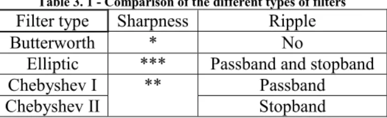
Table 3. 1 - Comparison of the different types of filters ... 52
Table 3. 2 - Power rejection versus elliptic filter order ... 52
Table 3. 3 - Minimum sampling rate allowed after splitting, with respect to Shannon’s theorem ... 55
Table 3. 4 - Minimum sampling rate allowed after splitting, in case of bandpass sampling without filtering ... 57
Table 3. 5 - Allowed bandwidth for Fs versus k ... 58
Table 3. 6 - Validity of inequality ... 58
Table 3. 7 - Recap table of allowed bandwidths for Fs, given k and M=2 ... 59
Table 3. 8 - Recap table of allowed bandwidths for Fs, given k and M=4 ... 59
Table 3. 9 - Recap table of allowed bandwidths for Fs, given k and M=8 ... 60
Table 3. 10 - Comparison of real and analytic signals ... 62
Table 3. 11 - Comparison between reference ADC and analytic signals with mixer ... 65
Table 3. 12 - Comparison between all architectures ... 66
Table 3. 13 - Examples of FoM ... 68
Table 3. 14 - Characteristics of [28] ... 69
Table 3. 15 - Estimation of power consumption for AGCs, QMs and ADCs ... 70
Table 3. 16 - Estimation of surface of the blocks ... 72
Table 3. 17 - Comparison of the architectures ... 73
Table.4. 1 - Performances with theoretical analog filters... 80
Table.4. 2 - Performances with actual analog filters ... 81
Table.4. 3 - Performances with actual analog filters ... 82
Table.4. 4 - Performances with measurement errors ... 83
Table.4. 5 - Performances with measured analog filters ... 86
Table E. 1 - Trade-off between Fs and filter orders for M=2 ... 101
Résumé
-10-
Résumé
Cette thèse est le fruit d’un partenariat entre la BL TVFE de NXP Semiconductors à Caen et l’ESIEE à Paris dans le cadre d’une thèse CIFRE. Le but est d’apporter une solution qui permette la réception simultanée de plusieurs canaux pour le câble.
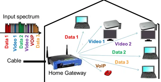
L’émission de la télévision est caractérisée par l’utilisation de larges canaux fréquentiels. Ainsi, la transmission de plusieurs canaux pour la télévision implique un spectre d’autant plus large. Une fonction tuner est actuellement directement implémentée sur la carte principale grâce à une solution totalement intégrée que sont les Silicon Tuners. NXP est l’un des leaders dans ce domaine. Cependant, c’est la réception simultanée de plusieurs flux de données qui sera la clé des produits du futur, pour la réception de la télévision par câble, satellite et par voie terrestre. C’est une caractéristique nécessaire pour avoir la possibilité de regarder une chaîne et d’en enregistrer une autre en même temps, ou la fonction Picture in Picture (PiP) par exemple. La tendance actuelle est de pouvoir recevoir plusieurs types de données grâce à un récepteur unique, une passerelle domestique (Home Gateway).
Fig. 1 - Passerelle domestique
Ceci implique la réception simultanée de plusieurs canaux situés aléatoirement dans toute la bande ou dans une partie de la bande RF. Pour recevoir ces canaux en même temps, il faut soit numériser toute la bande, soit implémenter autant de tuners de que chaînes que l’on souhaite recevoir. Le spectre correspondant à cette application s’étend de 50MHz à 1GHz et un cas d’usage serait de recevoir simultanément jusqu’à 16 canaux de 6MHz. Il est évident que l’implémentation de 16 tuners intégrés serait très coûteuse en termes de prix et de consommation. Il est donc crucial de rechercher des solutions qui permettent de numériser toute la bande de 1GHz. Pour réaliser une numérisation très large bande et très haute fréquence, un échantillonnage RF sera effectué le plus tôt possible dans la chaîne de réception, ce qui va limiter les composants RF et permettre une flexibilité au niveau de la sélection de l’information pertinente dans le domaine numérique (radio logicielle ou cognitive).
Cette recherche de flexibilité a un coût, notamment au niveau du Convertisseur Analogique-Numérique (CAN), point bloquant de la chaîne de réception, qui doit convertir une très large bande, à très haute fréquence (>2Gsps), avec une forte précision (>10 bits).
En effet, les performances des CAN classiques sont insuffisantes pour ce type de numérisation. Il est difficile d’avoir simultanément une vitesse élevée et une forte résolution.
Home Gateway Cable Input spectrum D ata 1 D ata 2 D ata 3 Vi d eo 1 Vi d eo 2 VOi P Data 1 Data 2 Data 3 Video 1 VoIP Video 2
Résumé
-11-
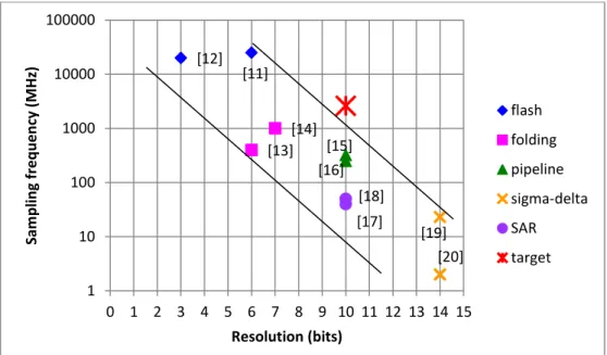
La figure ci-dessous présentée dans la partie 1, montre les performances que nous souhaitons obtenir par rapport à un bref état de l’art des CAN classiques.
Fig. 2 - Exemple d’état de l’art des CANs
D’après la littérature, les architectures parallèles semblent être une bonne solution à ce problème, comme l’entrelacement temporel et les bancs de filtres hybrides [1], présentés dans l’état de l’art de la partie 2. Une autre piste que nous proposons est de réduire les contraintes en divisant le spectre d’entrée en sous-bandes qui peuvent contenir un ou plusieurs canaux. Pour ce faire, il suffirait d’associer un banc de filtres analogiques et un banc de CANs. Une étude de cette architecture est réalisée dans la Partie 3 du manuscrit, ainsi que de plusieurs architectures utilisant différentes méthodes d’échantillonnage, comme l’échantillonnage passe-bande et l’échantillonnage complexe. L’échantillonnage passe-bande n’est pas adapté à notre cas car nous montrons qu’il faudrait découper notre spectre d’entrée large-bande en plus de 20 sous-bandes, ce qui aurait un coût non négligeable. En revanche, l’échantillonnage complexe permet de réduire la fréquence d’échantillonnage par deux, ce qui est avantageux dans une application large-bande. Il faut évaluer le coût des filtres polyphases ajoutés ainsi que du nombre de CANs qui est doublé. Une telle solution, basée sur l’utilisation des signaux analytiques et d’une conversion de fréquence semble intéressante, comme représenté sur la figure suivante :
Fig. 3- Architecture proposée
[11] [12] [13] [14] [15] [16] [19] [20] [17] [18] 1 10 100 1000 10000 100000 0 1 2 3 4 5 6 7 8 9 10 11 12 13 14 15 S am p li n g fr e q u e n cy (M H z) Resolution (bits) flash folding pipeline sigma-delta SAR target
Résumé
-12-
La fréquence d’échantillonnage est unique et commune à tous les CANs. Elle est également le double de la fréquence des oscillateurs locaux, ce qui simplifie la génération des fréquences. Le banc de filtres analogiques est composé de simples filtres elliptiques d’ordre 3, et les filtres polyphases ont des spécifications que l’on retrouve dans l’état de l’art. Cependant, la question du coût de cette architecture se pose et nous avons donc proposé d’introduire une fonction de coût générale qui relie la surface et la consommation, afin de comparer l’architecture proposée avec un CAN large-bande très haute performance, proche de nos spécifications. Ceci a été présenté à EuMW [2]. L’un des avantages de cette architecture est que tous les composants sont réalisables, même les CANs, et qu’il est possible d’éteindre des sous-bandes pour diminuer la consommation. Cette solution est intéressante pour le moment mais n’est pas compétitive en termes de consommation et de surface.
Nous proposons une alternative dans la partie 4, avec les Bancs de Filtres Hybrides (BFH). Nous étudions cette architecture, en gardant à l’esprit la faisabilité de la solution. Nous avons choisi un BFH à deux voies, avec un filtre analogique passe-bas et un passe-haut de type Butterworth et d’ordre 3 afin de limiter leurs coûts.
Fig. 4 - BFH à 2 voies
La fréquence d’échantillonnage des CANs est et le système est régi par les équations suivantes :
( )
( ) ( )
( ) ( ),
où et ( ) sont les transformées de Fourier de l’entrée et de la sortie du système. et sont les fonctions de transfert et de repliement, respectivement.
Le but de cette architecture est de numériser l’entrée , tel que l’on ait la sortie : ( )
à un gain et un déphasage linéaire près.
Pour cela, nous souhaitons avoir une fonction de transfert constante, ou même égale à 1, et une fonction de repliement nulle. Ceci dépend bien entendu du choix des filtres analogiques et numériques.
Résumé
-13-
Nous proposons un nouvel algorithme d’optimisation des filtres numériques, dits de synthèse, qui utilise à la fois les méthodes de Nelder-Mead et minimax, ainsi qu’une stratégie de perturbation pour éviter les minima locaux. Le critère à minimiser est ainsi :
| | | |
où est un coefficient qui donne plus d’importance à la réjection du repliement, qui est la plus difficile à minimiser. Le schéma de principe de cet algorithme est indiqué ci-dessous :
Fig. 5 - Algorithme d’optimisation
Nous nous sommes également intéressé au problème de la calibration, c’est-à-dire l’identification des filtres analogiques réels, et nous mettons en évidence l’impact de l’identification et des erreurs de mesure sur les performances de l’architecture. Ces résultats ont été présentés à Newcas [3]. Enfin, nous nous sommes attaché à réaliser un prototype d’une solution à base de BFH. Cette réalisation physique démontre la faisabilité de ce concept de réjection de repliement mais confirme aussi la sensibilité de cette architecture aux imperfections analogiques (ECCTD [4]).
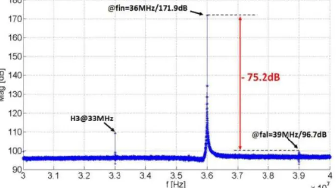
Pour cela, une carte avec deux CANs qui travaillent chacun à 75Msps et une carte avec un FPGA ont été utilisées, et les deux filtres analogiques ont été implémentés sur une troisième carte. Les mesures ont été réalisées sur une bande spectrale plus basses fréquences, pour s’adapter aux contraintes matérielles, mais cela permet tout de même de prouver le concept. Dans l’exemple ci-dessous, une sinusoïde de fréquence 36MHz est appliquée à l’entrée. Une raie correspondant au repliement est attendue à la fréquence 39MHz, à cause du sous-échantillonnage local. Celle-ci se trouve atténuée de plus de 75dB, ce qui correspond à l’objectif que nous nous étions fixé.
Résumé
-14- **************
Le travail technique de cette thèse a débuté par l’étude des architectures présentées dans la partie 3, basées sur un banc de filtres analogiques et d’un banc de CAN, puisque nous n’avons pas trouvé cette architecture dans la littérature. Cette étude, en sus de la familiarisation avec le contexte et la littérature, a duré environ un an. L’étude des BFH a également duré environ un an, et a précédé la réalisation du prototype, qui a quant à elle pris environ neuf mois. Il nous paraissait très important de conclure par une réalisation démontrant que les objectifs, en termes de performances, pouvaient être obtenus. Ceci s’est révélé techniquement très ardu et la rédaction n’a pas pu être terminée dans les temps. J’ai commencé une nouvelle aventure dans une start-up quelques jours à peine après la fin officielle de ma thèse. Notre premier projet était très important pour la survie de l’entreprise et a occupé une part très conséquente de mon temps cette année, ce qui a retardé encore l’achèvement de ce mémoire. Ce manuscrit termine donc ce travail de thèse.
Introduction
-15-
1 Introduction
This thesis is a partnership between the BL TVFE of NXP Semiconductors in Caen and ESIEE Paris. Its goal is to provide a solution to multi-channel reception for cable network. TV broadcasting is characterized by the use of wideband channels to transmit a large amount of information. Hence, multiple TV channels transmission requires a broadband spectrum. A tuner function is needed to select the desired channel among a large range of frequency for the demodulation. The tuner function is now implemented directly on the main board thanks to fully integrated solution, so-called Silicon Tuner. NXP are one of the leaders in this domain. Yet, multi-stream reception is a key point for future products in cable modem, terrestrial and satellite TV. This is a required feature for watch-and-record, picture-in-picture, or bonded channel applications... Another trend is the reception of different types of data using a unique receiver, called home gateway, as shown in Fig.1. 1.
Fig.1. 1 - Home Gateway
This implies simultaneous reception of several channels located anywhere on the whole band or partial RF band. The simultaneous reception supposes either the digitization of the whole band or the use of as many tuners as wanted channels. The spectrum of interest spreads from 50MHz to 1GHz, and one might want to simultaneously receive up to 16 channels of 6MHz. Of course, using for instance 16 tuners Integrated Circuits for receiving 16 channels will be severely over-killing in terms of cost and power. Therefore it is of particular importance to investigate solutions for the complete digitization of the 1GHz input spectrum.
Broadband digitization is a foreseen direction in RF sampling architecture: the whole RF band is sampled very early in the signal path. This reduces RF hardware, allows most of the processing to be done in digital domain, thus facilitates reconfigurability by software (Software Radio). Home Gateway Cable Input spectrum D ata 1 D ata 2 D ata 3 Vi d eo 1 Vi d eo 2 VOi P Data 1 Data 2 Data 3 Video 1 VoIP Video 2
Introduction
-16-
Fig.1. 2 - RF sampling architecture
However, this puts tough requirements on the Analog-to-Digital Converter (ADC): the wide signal bandwidth requires a high sampling rate (>2Gsps) ), while the lack of RF selectivity and the non-uniform input power spectral density (PSD) leads to high dynamic range requirement (>10bits).
The current Analog-to-Digital Converters architectures are not adapted to such an application. Flash ADCs, pipeline ADCs, Successive Approximation Register (SAR) ADCs and ΣΔ ADCs are either high speed or high resolution. According to the literature, parallel structures for ADCs are a key for the design of high-speed, high-resolution data converters. Time-interleaving (TI), Hybrid Filter Banks (HFB) are potential architectures [1]. Another possible way to cope with this problem is to divide the issues by splitting the spectrum into subbands. This architecture is called RFFB and consists of a bank of analog filters and a bank of ADCs. A study is proposed in Part 3, where we also propose and evaluate several architectures using different sampling methods such as bandpass sampling and complex sampling. A solution based on analytic signals and downconversion is promising. Then we introduce a general cost function that links surface and power consumption, in order to compare the proposed architecture with a wideband ADC close to our targets. This work has been presented at EuMW [2]. This architecture has the major advantage that all the components are feasible, even the ADCs, and it is possible to switch-off subbands to save power. It could be a good solution at the present time but it is not competitive in terms of power consumption and surface. An alternative is proposed in Part 4, where we study Hybrid Filter Banks. It is interesting to discover this architecture with realization feasibility in mind. This is why we select a 2-channel HFB with a 3rd-order Butterworth lowpass filter and a 3rd-order Butterworth highpass filter as low-cost analog filters. We present an original procedure for the optimization of the synthesis filters, which combines direct simplex search, minimax methods and a perturbation strategy to avoid local minima. We also address the calibration of the device, namely the identification of the actual analog filters, and highlight the impact of the identification and of measurement errors on the overall performances. This work has been presented at Newcas [3]. Finally, a physical realization proves the concept of aliasing rejection and confirms the parallel architecture sensitivity to analog mismatches. (ECCTD [4]).
We have started with the study of RFFB, because we have not found this architecture in the literature. This lasted around one year. Then the theoretical work on HFB preceeded the realization. It took around one year, and around 9 months respectively. The aim was to reach our targets and it was so challenging that the manuscript could not be finished on time. A few days and a conference later, I started a new adventure in another company, a start-up. Our first project was crucial for our survival and I spent much time on it this year. This manuscript ends this adventure.
Introduction
-17-
We continue this introduction with a brief presentation of the context of cable networks, which highlights the main figures and the objectives of our work.
Introduction
-18-
1.1 Cable network
1.1.1 Description (standards)
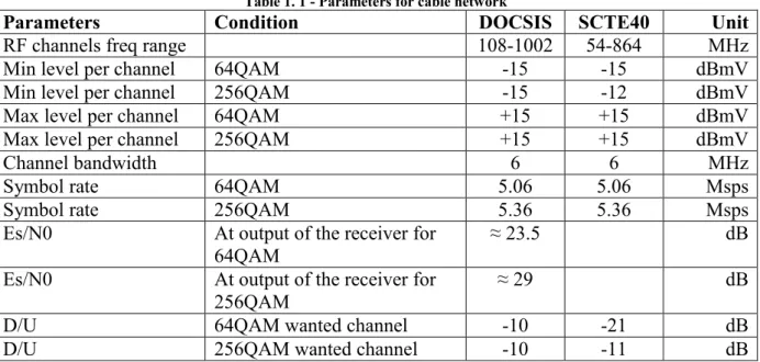
There are two main standards related to cable network, DOCSIS 3.0 [8] and SCTE40 [9], that meet the requirements of ITUJ83.B [10]. The main parameters that are necessary for the specification of our application are summarized in Table 1. 1:
Table 1. 1 - Parameters for cable network
Parameters Condition DOCSIS SCTE40 Unit
RF channels freq range 108-1002 54-864 MHz
Min level per channel 64QAM -15 -15 dBmV
Min level per channel 256QAM -15 -12 dBmV
Max level per channel 64QAM +15 +15 dBmV
Max level per channel 256QAM +15 +15 dBmV
Channel bandwidth 6 6 MHz
Symbol rate 64QAM 5.06 5.06 Msps
Symbol rate 256QAM 5.36 5.36 Msps
Es/N0 At output of the receiver for
64QAM
≈ 23.5 dB
Es/N0 At output of the receiver for
256QAM
≈ 29 dB
D/U 64QAM wanted channel -10 -21 dB
D/U 256QAM wanted channel -10 -11 dB
1.1.2 Signals
Some notions are defined in the following so as to introduce the specifications of the selected test case presented in 1.1.3.
1.1.2.1
is the SNR per channel wanted at the output of the ADC to be able to demodulate the channel. depends on the modulation of the channel and we can find its value in Table 1. 1.
Unlike the that is defined in the Nyquist band, i.e. from DC to , it is defined in a single channel (6MHz):
Introduction
-19- Fig.1. 3 - Es/N0
For now, we need to define the SNR per channel at the output of the ADC. We have to specify a margin to take into account the imperfections of the ADC.
1.1.2.2 Margin
We choose the Implementation Loss, , and calculate the corresponding Margin with the formula of APPENDIX A:
. (1.2)
Given that , .
Fig.1. 4 - Margin
1.1.2.3 Total Desired to Undesired power ratio
In cable network, the 6MHz wanted channel is located in a much wider band. The total power of the spectrum, , is calculated as follows. The power level of the wanted channel,
, can be determined using its relation in the standard with the adjacent undesired
channel. Thus, we have the total desired to undesired power ration, ⁄ .
⁄ . (1.3) 1.1.2.3.1 Calculation of total power of the spectrum
We consider the following spectrum. It is composed of blocks. For each one, we know the number of channels per block and the power of one channel, . The aim of this section is to calculate the total power of the whole spectrum, .
Introduction
-20-
We compute the total power of block , given the number of channels and the the power of each channel , in linear scale:
(1.4)
This is equivalent to the following equation, where and are the power of one channel in dB and the total power of block in dB, respectively:
( ) ( ) (1.5)
(1.6)
The total power of the whole spectrum is the sum of the total power of each block , in linear, as follows:
∑
(1.7) It is of course equivalent to the following equation, where and are the power of the whole spectrum in dB and the total power of block in dB, respectively:
( ) ∑ ( ) (1.8) ∑ ( ) . (1.9)
Now, let us consider a uniform flat spectrum, composed of channels, each of them with a power , as depicted in Fig.1. 6.
Fig.1. 6 - Spectrum with one block In this case, (1.9) becomes:
(
) (1.10)
(1.11) 1.1.2.3.2 Power of desired channel
Introduction
-21-
According to the standards, we know that the worst case of Ratio depends on the type of modulation of the desired and the undesired channels. Thus, we can determine the power of the Desired channel, , from the knowledge of the power of an adjacent channel, i.e. defined in 1.1.2.3.1, depending on the location of the wanted channel.
⁄ (1.12)
(1.13)
1.1.2.4 Crest factor
Crest Factor, , is a value that links the peak value and the root mean square value of a signal as follows:
(1.14) where is the signal magnitude.
For Multi-QAM modulations, is estimated to be 15dB, according to our simulations.
1.1.2.5 Backoff
Given that we reach the full-scale, backoff is null.
Fig.1. 8 -Wanted channel in the whole spectrum
1.1.2.6 Symbol Rate
The symbol rate, , is different from the channel bandwidth, , and they are linked as follows:
(1.15)
Where α is the roll-off factor. Fig.1. 9 highlights this difference:
Introduction
-22-
Fig.1. 9 - Symbol Rate versus channel bandwidth
The symbol rate depends on the modulation of the channel and is defined in ITU J.83.
1.1.3 Selected Test Case
This section presents the selected test case and explains the choices made on the input spectrum and the specifications of the wanted channel. Then, the most important values are calculated.
There are two main standards related to cable network, SCTE40 and DOCSIS 3.0, presented in 1.1.1. SCTE40 transmits a signal from 54MHz to 864MHz, whereas DOCSIS 3.0 transmits a signal from 111MHz to 1002MHz. To cover both, we choose to consider an input spectrum from to .
Our target is US, thus each channel has 6MHz-bandwidth, . We can calculate , the number of channels as follows:
(1.16)
(1.17)
Using the standard, we know that the power per channel is between -15dBm and 15dBm, i.e. between 45dBµV and 75dBµV. We choose the mean value: 60dBµV. We consider that the input spectrum is flat on the whole bandwidth. The possible tilt that reduces the power of channels at high frequencies can be compensated by adding an equalizer in the architecture. We are now able to calculate the total power of the input spectrum, .
As and , (1.11) gives
Introduction
-23-
As analog signals are becoming obsolete, we assume that the spectrum will be composed of digital channels, 256QAM for example. The wanted channel is also 256QAM. Fig.1. 10 sums up the hypotheses on the wanted signal and the input spectrum.
The power ratio of the Desired to the adjacent undesired channel, , in the worst case, is not indicated for this example in SCTE40. It is possible to evaluate it using the standard values.
The desired and the undesired signals are 256QAM with a nominal level of -5dBc. In the worst case, the wanted signal will be at its weakest level, 6dB below nominal level which itself may be -2dB below -5dBc (-5-2-6= -13dBc), and the unwanted will be at its strongest level, 6dB above nominal, which itself may be 2dB above -5dBc (-5+2+6=3dBc). Thus, the undesired 256QAM signal is 16dB stronger than the desired 256QAM signal in the worst case. As a reasonable value, we choose .
Given that the level of the adjacent is 60dBµV, the wanted channel’s level, , is
49dBµV ( ).
As a consequence, (1.3) gives ⁄ .
The choice of 256QAM implies that ⁄ should be 29dB and that the symbol rate, , is 5.36Msym/s, that corresponds to a roll-off factor of 0.12.
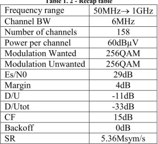
Table 1. 2 summarizes the values that will be used to specify the ADC Signal-to-Noise ratio (SNR) on the Nyquist band (see 1.3.2).
Table 1. 2 - Recap table
Frequency range 50MHz 1GHz
Channel BW 6MHz
Number of channels 158
Power per channel 60dBµV
Modulation Wanted 256QAM
Modulation Unwanted 256QAM
Es/N0 29dB Margin 4dB D/U -11dB D/Utot -33dB CF 15dB Backoff 0dB SR 5.36Msym/s 1.2 Applications
TV broadcasting is characterized by the use of wideband channels to transmit a large amount of information. Hence, multiple TV channels transmission requires a broadband spectrum. A tuner function is needed to select the desired channel among a large range of frequency for the demodulation. The tuner function is now implemented directly on the main board thanks to fully integrated solution, so-called Silicon Tuner. NXP semiconductor has demonstrated the feasibility of Silicon tuner solution currently in mass-production and is the leader in this field. Multi-stream reception is a key point for future products in cable modem. This implies simultaneous reception of several channels located anywhere on the whole or partial RF band.
Introduction
-24-
The first part of this section briefly presents the architecture of a single tuner for cable modem and the second part introduces the constraints associated to multi-channel reception.
1.2.1 Single cable tuner
NXP Semiconductors are the leaders in Silicon Tuners. We know how to receive only one channel.
The global architecture is depicted on Fig.1. 11. The principle is to select the wanted channel located anywhere in the whole spectrum, with a bandpass filter (Fig.1. 12), to down-convert it near DC with a mixer and to filter harmonics with a lowpass filter (Fig.1. 13). Then, the wanted channel is converted from analog to digital with an ADC, and it is demodulated using a DSP.
Fig.1. 11 - Common and simplified receiver architecture
Fig.1. 12 - Selection of the wanted channel with BPF
Fig.1. 13 - Wanted channel after mixing and LPF
Introduction
-25-
1.2.2 Multi-channel reception
To receive several channels simultaneously, we can obviously imagine having a tuner per channel (Fig.1. 14).
Fig.1. 14 - M multiple common receivers in parallel Yet, this solution is overkilling in terms of cost and power.
Today, one foreseen direction is RF sampling architecture: whole RF band is sampled very early in the signal path, as shown on Fig.1. 15. This reduces RF hardware, allows most of the processing (mixing, filtering) to be done in digital domain, thus facilitates reconfigurability by software (Software Radio). ADC becomes the bottleneck of such architecture, because it needs to be broadband and must cope with the whole input dynamic range. The following section derives the specifications of this ADC according to the selected test case in 1.1.3.
Introduction
-26-
1.3 ADC specifications
An ADC is specified by its sampling rate, , and the SNR in the Nyquist band, .
1.3.1 Sampling rate
In general, the sampling rate should be chosen so as to fulfill the Shannon’s condition to avoid aliasing. According to the selected test case, the sampling rate should be greater than 2Gsps. Moreover, to avoid MoCA, we choose .
1.3.2 SNR on the Nyquist band
is the signal-to-noise ratio defined on the Nyquist band with a full-scale input sinus.
In 1.1.2, we have calculated the ADC noise in 6MHz. We need to define the noise in the Nyquist band.
The oversampling gain, , links noise in two different bandwidths, and :
( ) (1.18)
where and , according to the previous sections.
Introduction
-27- Here is the corresponding level diagram:
Fig.1. 17 - Level diagram
From Fig.1. 17, we deduce equation (1.19) and the minimum required SNR in Nyquist band for this ADC working at 2.6GHz, that is around 55dB, according to the selected test case.
⁄ ⁄ ( ) (1.19)
1.4 Conclusion
In the context of multi-channel reception for cable modem, broadband digitization is the major issue and, thus, the ADC is the bottleneck of architecture of RF sampling. We have specified an ADC that should be working at 2.6GHz, with a required SNR greater than 55dB to be able to digitize the selected input spectrum, which is really challenging. This input spectrum has been chosen to meet the requirements of the standards SCTE40 and DOCSIS 3.0.
State-of-the art
-28-
2 State-of-the-art
In the introduction, we have specified the ADC that is the bottleneck of the receiver in case of multi-channel reception. According to the selected test case, we need an ADC working at 2.6GHz with a minimum required SNR of 55dB. As shown in the following section that sketches the state-of-the-art of stand alone ADCs, it is really challenging. Then, we will see that parallel architectures seem to be necessary to reach the ADC requirements, as the constraints on each subband ADC can be relaxed. Finally, some sampling methods are recalled such as bandpass sampling and complex sampling since they are solutions that reduce the sampling frequency below the Nyquist rate in particular conditions.
2.1 Stand-alone ADC
There are several types of ADCs, the most famous being flash, folding, pipeline, sigma-delta and SAR. They can be classified as in Fig.2. 1 regarding their speed, i.e. input signal bandwidth, and their resolution, i.e. the number of bits needed to convert the signal from analog to digital. Therefore, we have the following graph:
Fig.2. 1 - Trade-off of ADCs
2.1.1 Flash
2.1.1.1 Architecture
Flash ADCs (sometimes called “parallel” ADCs) are typically high-speed, low resolution. Flash ADC is the fastest architecture available. A flash ADC is made up of a large bank of comparators. An N-bit flash ADC consists of 2N resistors and 2N-1 comparators. So the number of comparators goes up by a factor of 2 for every extra bit of resolution. This leads to high power consumption. In addition, the capacitive load seen by the sample-and-hold is quite high. Fig.2. 2 shows the architecture of a 3-bit Flash ADC, thus with 8 resistors and 7 comparators.
State-of-the art
-29-
Fig.2. 2 - 3-bit Flash ADC architecture
2.1.1.2 Principle
Each comparator has a reference voltage from the resistor string which is 1 LSB higher than that of the one below in the chain. For a given input voltage, all the comparators below a certain point will have their input voltage larger than their reference voltage and a “1” logic output, and all the comparators above that point will have a reference voltage larger than the input voltage and a “0” logic output. The 2N
-1 comparator outputs therefore behave in a way analogous to a mercury thermometer, and the output code at this point is sometimes called a “thermometer” code. Since 2N
-1 data outputs are not really practical, they are processed by a decoder to generate an N-bit binary output.
2.1.1.3 State-of-the-art
For example, we find in the literature a 6-bit flash ADC working at 25Gsps in 90nm CMOS [11], or even a 3-bit flash ADC working at 20Gsps in 65nm CMOS [12].
2.1.2 Folding
2.1.2.1 Architecture
Folding ADCs have approximately the same architecture as flash ADCs. They consume less power than flash, as depicted on Fig.2. 3.
State-of-the art
-30-
Fig.2. 3 - Flash versus Folding
The architecture of a folding analog-to-digital converter system for an 8-bit ADC is shown on Fig.2. 4:
Fig.2. 4 - Folding architecture
There are a fine quantization for LSBs and a coarse quantization for MSBs. The fine quantization is done by a 4-bit Flash ADC preceeded by a folding circuit, whereas the coarse quantization is done by a 4-bit Flash ADC, in this example.
2.1.2.2 Principle
The most significant bits are determined by the coarse quantizer, which determines the number of time a signal is folded. The fine bits are determined by the fine quantizer which converts the pre-processed “folded” signal into the fine code. In this way it is possible to obtain an 8-bit resolution with only 30 comparators (4-bit coarse plus 4-bit fine), instead of 255 comparators for a Flash ADC. The low component count results in a small die area, while more power can be spent into the system to extend the bandwidth of the comparator and folding stages resulting in a higher sampling speed and a larger analog input bandwidth. On the other hand, a reduction in power can be obtained when sampling rate and analog input bandwidth are fixed.
On Fig.2. 5, there are the input signal (top) and the corresponding output signal of the folding stage (bottom) as a function of time. The result of the operation is an output signal with a frequency that is a multiple of the input frequency.
State-of-the art
-31-
Fig.2. 5 - Folding principle
2.1.2.3 State-of-the-art
For example, we find in the literature a 6-bit folding ADC working at 400Msps in 90nm CMOS [13] or even a 7-bit folding ADC working at 1Gsps in 65nm CMOS [14].
2.1.3 Pipeline
2.1.3.1 Architecture
Pipelined ADCs are typically medium-speed, high resolution.
A pipelined ADC employs a cascaded structure in which each stage works on one to a few bits (of successive samples) concurrently. Although it cannot work very fast (~100Msps), it does not consume much.
The pipelined ADC had its origins in the sub-ranging architecture. Fig.2. 6 shows an example of pipeline architecture:
Fig.2. 6 - Pipeline architecture
2.1.3.2 Principle
The input is first converted by a simple 3-bits flash ADC. The digital value is converted back in analog format by a 3-bit DAC and subtracted from the input, this gives a residue. The residue is multiplied to get the full range, and then converted by as second flash.
In Fig.2. 6, the analog input, VIN, is first sampled and held steady by a sample-and-hold
(S&H), while the flash ADC in stage one quantizes it to three bits. The 3-bit output is then fed to a 3-bit DAC (accurate to about 12 bits), and the analog output is subtracted from the input.
State-of-the art
-32-
This "residue" is then gained up by a factor of four and fed to the next stage (Stage 2). This gained-up residue continues through the pipeline, providing three bits per stage until it reaches the 4-bit flash ADC, which resolves the last 4LSB bits. Because the bits from each stage are determined at different points in time, all the bits corresponding to the same sample are time-aligned with shift registers before being fed to the digital-error-correction logic. Note when a stage finishes processing a sample, determining the bits, and passing the residue to the next stage, it can then start processing the next sample received from the sample-and-hold embedded within each stage. This pipelining action is the reason for the high throughput.
2.1.3.3 State-of-the-art
For example, we find in the literature a 10-bit pipeline ADC working at 320Msps in 90nm CMOS [15] or even a 10-bit pipeline ADC working at 250Msps in 90nm CMOS [16].
2.1.4 SAR
SAR means Successive Approximation Register. They represent the majority of the ADC market for medium to high resolution ADCs. Yet, they do not work very fast. As it only needs 1 comparator for N bits, power consumption is very low.
2.1.4.1 Architecture
A SAR ADC consists of a track-and-hold, a comparator, an n-bit DAC and SAR logic.
Fig.2. 7 - SAR structure
2.1.4.2 Principle
The basic principle of a SAR ADC is to convert the input voltage by successively approaching it (binary search algorithm).
First of all, the analog input voltage VIN is held on a track-and-hold. To implement the binary
search algorithm, the N-bit register is first set to midscale (FS/2). This forces the DAC output VDAC to be VREF/2, where VREF is the reference voltage provided to the ADC. A comparison is
then performed to determine if VIN is less than or greater than VDAC. If VIN is greater than
VDAC, the comparator output is logic high or ‘1’ and the MSB of the N-bit register remains at
‘1’. Conversely, if VIN is less than VDAC, the comparator output is logic low and MSB of the
register is cleared to logic ‘0’. The SAR control logic then moves to the next bit down, forces that bit high, and does another comparison. The sequence continues all the way down to the
State-of-the art
-33-
LSB. Once this is done, the conversion is complete, and the N-bit digital word is available in the register.
Fig.2. 8 shows an example of a 4-bit conversion. The y-axis (and the bold line in the figure) represents the DAC output voltage. In the example, the first comparison shows that VIN <
VDAC. Thus bit 3 is set to ‘0’. The DAC is then set to (0100)2 and the second comparison is
then performed. As VIN > VDAC, bit 2 remains at ‘1’. The DAC is then set to (0110)2, and the
third comparison is performed. Bit 1 is set to ‘0’, and the DAC is then set to (0101)2 for the
final comparison. Finally, bit 0 remains at ‘1’ because VIN > VDAC.
Fig.2. 8 - SAR operation (4-bit ADC example)
Notice that four comparison periods are required for a 4-bit ADC. Generally speaking, an N-bit SAR ADC will require N comparison periods and will not be ready for the next conversion until the current one is complete. This explains why these types of ADCs are power- and space-efficient.
2.1.4.3 State-of-the-art
For example, we find in the literature a 10-bit SAR ADC working at 40Msps in 0.13µm CMOS [17] or even a 10-bit SAR ADC working at 50Msps in 90nm CMOS [18].
2.1.5 ΣΔ
Traditional sigma-delta type converters have limited bandwidth, whereas they reach high resolution and they do not consume much.
2.1.5.1 Architecture
A sigma-delta ADC consists of an integrator, an n-bit flash ADC, an n-bit DAC, a digital filter and a decimator. Fig.2. 9 shows an example of a sigma-delta ADC.
State-of-the art
-34-
Fig.2. 9 - Multi-bit sigma-delta ADC
2.1.5.2 Principle
Assume a dc input at VIN. The integrator is constantly ramping up or down. The output of the
comparator is fed back through an n-bit DAC to the summing input. The negative feedback loop from the comparator output through the n-bit DAC back to the summing point will force the average dc voltage to be equal to VIN. This implies that the average DAC output voltage
must equal the input voltage VIN. The average DAC output voltage is controlled by the
ones-density in the data stream from the comparator output. As the input signal increases towards +VREF, the number of “ones” in the serial bit stream increases, and the number of “zeros”
decreases. From a very simplistic standpoint, this analysis shows that the average value of the input voltage is contained in the serial bit stream out of the comparator. The digital filter and decimator process the serial bit stream and produce the final output data.
2.1.5.3 State-of-the-art
For example, we find in the literature a 14-bit sigma-delta ADC working at 23Msps in 90nm CMOS [19] or even a 14-bit sigma-delta ADC working at 2Msps in 0.18µm CMOS [20].
2.1.6 Conclusion
Fig.2. 10 depicts the few references of ADCs we have just mentioned. We can notice that it looks like Fig.2. 1. We also see that the targeted ADC (red star) is faster and/or with a better resolution than these ADCs.
State-of-the art
-35-
Fig.2. 10 - Example of state-of-the-art of ADCs
2.2 Parallel structures
Parallel architectures seem to be a solution to broadband digitization. In literature, we find structures such as Fig.2. 11:
Fig.2. 11 - Parallel architecture
We wish to digitize the input signal x(t) at the global sampling rate . The analog input signal is split into M subbands { }. Then each subband signal is converted at by the subband ADCs. Finally, the undersampled signals, { } are recombined in such a way that the digital output is equivalent to the analog input , sampled at . Thus, the constraints on the subband ADCs are reduced compared to a single high-performance ADC.
[11] [12] [13] [14] [15] [16] [19] [20] [17] [18] 1 10 100 1000 10000 100000 0 1 2 3 4 5 6 7 8 9 10 11 12 13 14 15 S am p li n g fr e q u e n cy (M H z) Resolution (bits) flash folding pipeline sigma-delta SAR target
State-of-the art
-36-
Two main parallel architectures will be described in the following sections: time-interleaving and hybrid filter banks. Parallel sigma-delta are not studied here ([21], [22], [23]).
2.2.1 Time-Interleaving
The first studied and the most famous parallel architecture is time-interleaving [24], [25]. Fig.2. 12 depicts the architecture.
Fig.2. 12 - Time-interleaving architecture
There are M ADCs in parallel so each ADC works at , as explained before. Thus the ADCs sample at the same sampling rate but at different instants, { }, because of phase shifting from one branch to another, as depicted on Fig.2. 13. Then, after sampling, a multiplexer recombines the samples to have the output signal. The global resolution is theoretically equivalent to the resolution of each sub-ADC.
State-of-the art
-37-
So the global sampling rate is Fig.2. 14 represents the time-interleaving architecture in the general framework of parallel architecture.
Fig.2. 14 - Principle of time-interleaving
In practice, the quantizers are different from each other. There are four types of errors: offset errors, gain errors, phase errors and timing errors. Some methods have been proposed to correct these errors in [25], [26], [27].
NXP Semiconductors is working on this architecture and has reached high-performance such as a SNDR of 48.5dB with a sampling rate of 2.6 Gsps [28]. There are 64 SAR ADCs in parallel, each ADC working at around 40Msps.
2.2.2 Spectral decomposition: HFB
We can split the input spectrum into several subbands thanks to analog filters, called analysis bank. Then, each subband signal is sampled thanks to subband ADCs that work at a lower sampling rate than the global sampling rate. Upmixers and digital filters composed the synthesis bank and finally, the subbands are recombined. This architecture is called Hybrid Filter Banks (HFB) and can be implemented with either discrete-time or continuous-time analog filters.
2.2.2.1 Discrete-time Hybrid Filter Banks
Fig.2. 15 depicts a discrete-time Hybrid Filter Bank (DT-HFB).
State-of-the art
-38-
We suppose that the input signal is bandlimited. The analysis bank is composed of discrete-time analog filters , ,…, , such as switched-capacitors. The input signal is first sampled and then filtered by discrete analog filters , ,…,
. Then, the signals , ,…, are downsampled and quantified at the
sampling rate , where is the global sampling rate and M is the number of subbands. After that, the individual signals are up-sampled and filtered by the digital filters , ,…, . Finally, the signals are added and the digital output is a
digital equivalent to the analog input signal.
The advantage of the discrete-time HFB is that the switched-capacitors filters can be implemented with a very good precision, compared to continuous-time analog filters. A disadvantage of this structure is that the sampling of the input signal should be done at the global sampling rate, which is very high in our applications. Another limitation of the discrete-time filters is their maximum frequency.
DT-HFB has been studied in [29] for the first time. The impact of quantization at the output of DT-HFB-based ADC has been studied in [30]. An analysis of the impact of analog imperfections on the DT-HFB performances has been proposed in [31] or [32].
2.2.2.2 Continuous-time Hybrid Filter Banks
Fig.2. 16 depicts a continuous-time Hybrid Filter Bank (CT-HFB).
Fig.2. 16 - Continuous-time Hybrid Filter Bank
This structure has been proposed in [33]. In this case, the analog input signal is directly decomposed by the continuous-time analog filters , ,…, . We suppose that is bandlimited. Then, the M filtered signals are sampled at a sampling rate
, where is the global sampling rate and M is the number of subbands. This differs from the case of DT-HFB where the input signal had to be sampled at the global sampling rate. After that, the digital signals , ,…, are quantified, upsampled and filtered by the digital filters , ,…, . Finally, the output results from the addition of the signals at the output of the digital filters. We choose the analog filters and the digital filters such that the output is as close as possible to the analog input signal.
State-of-the art
-39-
The advantage of this architecture with continuous-time analog filters is that we can work at high frequencies, compared to switched-capacitors. The major disadvantage is the sensitivity to realization errors, compared to discrete-time filters.
Many articles on continuous-time hybrid filter banks have been issued. A frequency analysis of HFB can be found in [34], [35] and [36]. Many synthesis methods for 2-channel HFB have been proposed in [34], [37], [38], [39], [40], [41]. Synthesis methods for more than 2 subbands are in [36], [42], [43].
In [44] and [45], ideal transfer functions of analog filters have been calculated from a discrete-time HFB. Quantization noise is studied in [34]. An analysis of mismatches between the subband ADCs is proposed in [34], [36] and [46]. Some design techniques have been patented by Velazquez [47], [48], [49].
[50], [51], [52], [53], [54], [55] [56] are Supélec’s contributions to synthesis methods with realization constraints. There are some examples of 8-channel HFB.
2.2.3 Conclusion
As Time-Interleaving architectures are well-covered in literature, we will focus on HFB in Part 4. Yet, there is another intuitive architecture that does not appear in literature. It consists in splitting the input spectrum into subbands and simply converting the subbands. We propose a study of this architecture in Part 3. In this part, we will need many sampling methods. They are recalled in the following section.
2.3 Sampling
ADCs have two functions: sampling and quantizing. In this section, we focus on sampling that is the process of going from continuous-time signals to discrete-time signals.
Fig.2. 17 shows a sampler that samples the continuous-time signal at the sampling period .
Fig.2. 17 - Sampler
2.3.1 Introduction
Ideal sampling process does not cause any information loss, provided the Shannon condition is fulfilled.
A real signal, from to , with a bandwidth , must be sampled at a rate chosen to avoid aliasing:
(2.1)
is called the Nyquist rate. In case of a baseband signal, we have , so (2.1) is equivalent to:
State-of-the art
-40-
Yet, for some applications we prefer having a sampling rate much greater than the Nyquist rate. Indeed, oversampling could be useful to relax the anti-aliasing filter, or decrease the white noises (quantization, kT/C…) density in the wanted channel bandwidth by spreading these noises over a wider bandwidth.
2.3.2 Bandpass sampling
Bandpass sampling is applied to bandpass signals. It can downconvert a signal without any mixer.
2.3.2.1 Bandpass sampling of a bandpass signal
In [57], the theory of bandpass sampling is explained. We consider a bandpass signal as follows:
Fig.2. 18 - Bandpass signal description
The bandpass signal is located between and . Its bandwidth is . is the sampling rate. We notice that is lower than . Yet, should be carefully chosen to avoid aliasing.
Fig.2. 19 - Bandpass sampling Sampling rates should fulfill the following equations:
(2.3)
(2.4)
State-of-the art -41- (2.6) (2.7)
We notice that (2.7) is equivalent to Shannon’s theorem for k = 0:
(2.8)
From (2.7), we can determine allowed and disallowed bands for . Indeed, each allowed band has a width that depends on k:
(2.9)
(2.10)
Thanks to (2.10), we see that (2.7) is true while k respects:
( ) (2.11)
Furthermore, we can evaluate the bandwidth of disallowed bands that also depends on k:
(2.12)
(2.13)
Fig.2. 20 gives an example of allowed and disallowed bands for .
Fig.2. 20 - Allowed (green) and disabled bands
2.3.2.2 Bandpass sampling of contiguous spectra
Bandpass sampling could also be applied to a bandpass signal that is adjacent to other unwanted signals, as in [58] where a shift of the desired subband is proposed so that there is no need for RF bandpass filters at the front-end.
Let‘s introduce the notation and adapt them to our case:
Fig.2. 21 - Contiguous spectra of a set of N RF signals from [58]
As explained in [58], we consider a set of N RF signals and the ith one is located between Hz and Hz with a bandwidth of , where i =1,2…N. The ith RF signals can be
State-of-the art
-42-
denoted as and negative spectrum , where i =1,2….N. As a whole, these N RF signals can be denoted as , with the positive spectrum and negative spectrum . For the sake of simplicity, assume that the spectrums of these multiple RF signals are contiguous, i.e. , where i = 1,2…N -1, as depicted in Fig.2. 21.
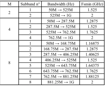
In our case, we have M contiguous RF signals: the M subbands. corresponds to the whole input spectrum, so , and . As we consider M subbands with equal bandwidths, we have:
(2.14)
Fig.2. 22 depicts the spectrums of the N RF signals and their replicas after sampling.
Fig.2. 22 - Spectra of the N RF signals and their replicas after sampling from [58] To cause no aliasing, we should fulfill the following conditions:
(2.15)
(2.16)
In [58], one also defines:
(
) (2.17)
And the minimum valid sampling frequency for the ith RF signal is given by:
(2.18)
So, the higher , the lower .
State-of-the art
-43-
2.3.3 Complex sampling
2.3.3.1 Euler equations
We recall here the expression of a cosinus and a sinus at the frequency :
(2.19)
(2.20) Fig.2. 23 depicts the corresponding plots ((2.19) and (2.20)), in both time and frequency domain:
Fig.2. 23 - Representation of sinus and cosinus in time and frequency domain If we multiply the sinus by , that is equivalent to shift by , we have:
(2.21)
Then, we find the Euler’s equation by adding (2.19) and (2.21):
(2.22)
Fig.2. 24 depicts the corresponding plots in frequency domain:
State-of-the art
-44-
In other words, in complex domain, it is possible to avoid negative frequencies.
In our example, the input signal is real, thus its spectrum is symmetric, as depicted in Fig.2. 25:
Fig.2. 25 - Real input spectrum
The corresponding graph with a complex input spectrum is depicted in Fig.2. 26:
Fig.2. 26 - Complex input spectrum
2.3.3.2 Hilbert transform
A signal which has no negative frequency components is called an analytic signal. The real-to-complex transformation is called the Hilbert transformation.
A filter can be constructed which shifts each sinusoidal component by a quarter cycle. This is called a Hilbert transform filter, such as, for example, Passive Polyphase Filters (PPF) that suppress or at least, attenuate much negative frequencies. This type of filters will be mentioned in Part 3.
So, when a real signal and its Hilbert transform are used to form a new complex signal , the signal is the (complex) analytic signal corresponding to the real signal .
As an example, if we have:
(2.23)
then ( ) (2.24)
and (2.25)
We find the Euler’s equation again.
Fig.2. 27 shows the block diagram for complex sampling with the Hilbert filter and two ADCs.
Fig.2. 27 - Block diagram for complex sampling
Thus, thanks to filters as polyphase filters, negative frequencies can be suppressed. This has obviously an impact on the choice of the sampling rate.