HAL Id: hal-03010263
https://hal.archives-ouvertes.fr/hal-03010263
Submitted on 4 Jan 2021
HAL is a multi-disciplinary open access
archive for the deposit and dissemination of
sci-entific research documents, whether they are
pub-lished or not. The documents may come from
teaching and research institutions in France or
abroad, or from public or private research centers.
L’archive ouverte pluridisciplinaire HAL, est
destinée au dépôt et à la diffusion de documents
scientifiques de niveau recherche, publiés ou non,
émanant des établissements d’enseignement et de
recherche français ou étrangers, des laboratoires
publics ou privés.
Observed by Scanning Tunneling Microscopy
O. Šofranko, R. Leriche, A.P. Morales, T. Cren, S. Sasaki, L. Cario, P. Szabo,
P. Samuely, T. Samuely
To cite this version:
O. Šofranko, R. Leriche, A.P. Morales, T. Cren, S. Sasaki, et al.. Periodic Surface Modulation of
(LaSe) 1.14 (NbSe 2 ) Observed by Scanning Tunneling Microscopy. Acta Physica Polonica A, Polish
Academy of Sciences. Institute of Physics, 2020, 137 (5), pp.785-787. �10.12693/APhysPolA.137.785�.
�hal-03010263�
Periodic surface modulation of (LaSe)1.14(NbSe2) observed by scanning tunneling microscopy.
O. ŠOFRANKO*1, R. LERICHE3, A.P. MORALES3, T. CREN3, S. SASAKI2, L. CARIO2, P. SZABO1,
P. SAMUELY1and T. SAMUELY1
1
Centre of Low Temperature Physics, Institute of Experimental Physics SAS, and P. J. Šafárik University, 040 01, Košice, Slovakia
2
Institut des Matériaux Jean Rouxel (IMN), Université de Nantes, CNRS, 2 rue de la Houssinière, BP 32229, 44322 Nantes Cedex 3, France
3
Sorbonne Université, CNRS, Institut des Nanosciences de Paris, UMR7588, F-75252, Paris, France
Fourier transformation of atomically resolved STM topography of (LaSe)1.14(NbSe2) revealed a surface
modulation along the triangular crystal lattice of NbSe2 layer, but with a two times larger period. We
compare it to the modified charge density wave found on plain NbSe2under strain.
Keywords: scanning tunneling microscopy, misfit layer compound, Lanthanum niobium selenides, electronic properties
1. Introduction
The layered transition metal dichalcogenides (TMD), TX2, where T is the early transition metal and X is S, Se or Te, are remarkable compounds due to their fascinating physical properties. They can accommodate various physical phenomena, such as the charge density waves (CDWs) and superconductivity [1–3]. Though TMDs with 1T structure could be superconducting only by doping or external pressure [4,5],TMD materials with 2H structure, e.g. 2H-NbSe2, exhibit intrinsic
superconductivity [6,7]. Their two-dimensional structure is an important feature giving rise to e.g. Ising or topological superconductivity [8,9].
Transition-metal dichalcogenides (TMDs) are the promising candidates for tuning their properties by inducing strain. They can withstand up to 10 % of in-plane strain before breaking, thus providing enough space for engineering new strain induced properties [10]. Charge density wave (CDW) is one of the emergent states occurring in TMDs [10] often accompanied by other, possibly competing phases.
*
In the case of 2H-NbSe2 superconductivity (Tc = 7.2 K) meets triangular (3Q) charge density wave phase
(TCDW = 33 K) [2]. Exact mechanisms driving the choice of particular CDW wavevector remains
unanswered even though various mechanisms have been proposed [11–16].
Small strain-induced changes in the electronic band structure and phonon dispersion can lead to dramatic change in CDW wavevector and geometry [17]. Single crystal attached to the silica plate at room temperature can be stretched while cooling down to 4 K because of mismatch between their thermal expansion coefficients. Shang Gao et al. induced strain in 2H-NbSe2 via this method and observed change
of CDW period. In addition to the well-known CDW ordering of ~ 3a0 period (below 33 K), where a0 is
the triangular NbSe2 lattice constant, they observed two additional CDW phases, unidirectional "stripe"
(1Q) CDW ordering with 4a0 period and a triangular (3Q) ordering with 2a0 period. The wavevectors of
all observed CDWs were found to be oriented along Γ-M direction. Presence of various CDW phases in different regions of sample was attributed to inhomogeneous strain [17].
Misfit compounds are based on alternating hexagonal TMDs and square MX lattice, where M can be for example Sn, Pb or La. They have peculiar structure arising from stacking layers with different lattice types. Lattice mismatch results in variety of physical properties misfit compounds can have. There are misfit materials in which we can observe superconductivity and CDWs. The single-crystalline misfit compound (LaSe)1.14(NbSe2) has been successfully synthesized in the 90s [18]. It is possible to grow very
good superconductive (Tc = 1.2K) single crystals with RRR close to 6. It is expected that vertically
stacked TMDs are strongly affected by strain [19,20].
Here we report the observation of surface modulation on (LaSe)1.14(NbSe2)with period ~ 2a0,
commensurate with the crystal lattice. This observation correlates to the strain induced change of CDW order parameter in pure NbSe2.
2. Preparation of experiment
Scanning tunneling microscopy (STM) experiments were carried out by means of the Specs JT STM system operated in ultra-high vacuum (10-10 mbar). Atomically sharp Au STM tips were formed ex
situ by electrochemical etching followed by Ar+ sputtering and annealing in situ.
(LaSe)1.14(NbSe2) samples have layered structure with weak iono-covalent bonds between layers,
which enables easy cleaving procedure. The sample was glued to a molybdenum sample holder, conductively connected by silver paste. We glued a thin metal stripe to the top layer of the sample. By removing the metal stripe in situ prior to the STM experiment, we exfoliated the upper layers, thus
achieving an atomically flat surface without contaminations. Moreover, during the cleavage, the sample was placed on the liquid nitrogen shield of the refrigerator. This way we were able to obtain larger atomically flat terraces compared to the cleaving procedure at room temperature.
Surface topography was acquired in the constant current mode with the set point current Iset = 50
pA. Bias voltage Vbias= 100 mV was applied to the sample while the tip was grounded. Both the STM
head and sample were kept at 1.2 K.
3. Results
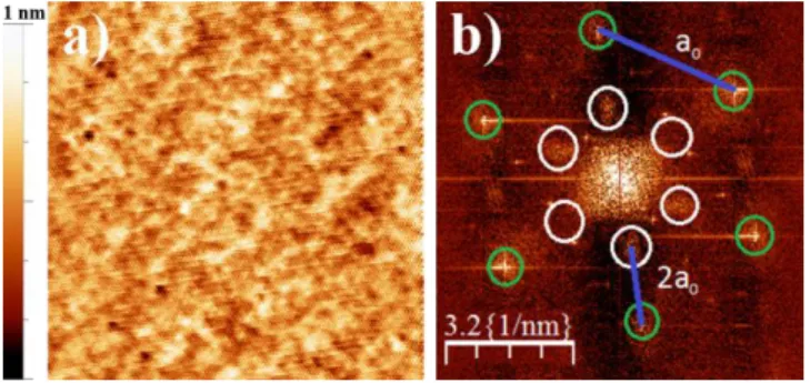
Although it is not clear in advance which of the two planes will terminate the surface of the (LaSe)1.14(NbSe2) monocrystal after cleavage, STM topography (Fig. 1 left) reveals a triangular lattice.
LaSe layer has square crystal structure; therefore, we assume that the surface is terminated by the NbSe2
layer. In addition to the triangular lattice of individually resolved Nb atoms characteristic for the NbSe2
surface, the topography reveals a plethora of elevated or depressed areas. To facilitate the analysis of these intricate patterns, we employed the two-dimensional Fourier transform (FT). The evident six atomic Bragg peaks of the FT, marked by the green circles in figure 1b, correspond to the triangular NbSe2 lattice
with period a0. Notably, another distinct feature appears halfway along two of the three Bragg vectors, i.e.
along the Γ- M directions. This surface modulation with period ~ 2a0, marked by white circles in Fig. 1b,
is strongly reminiscent of the triangular (3Q) CDW ordering with 2a0 period observed by Gao et al. on
NbSe2 under strain [17].
Fig. 1: a) STM topography image (32 x 32 nm2), color corresponds to the height according to the colorbar on the left. b) Fourier transform of the topography. Bragg peaks in green circles have lattice constant a0,
areas representing period ~ 2a0 are marked by white circles.
To better illustrate this surface modulation, we extracted the relevant FT peaks, namely the Bragg peaks and the peaks corresponding to the 2a0 modulation in one direction (Fig. 2a). Fig. 2b, a zoom of the
atomic row, i.e. 2a0 period, is elevated. Still, while Gao et al. observed this modulation along all thee
Bragg vectors, in our case one pair of the FT peaks is missing. Possibly, the peaks in this direction are suppressed by the adjacent focused sharp peaks. Several of these sharp peaks, as well as a long-range modulation represented by a bright spot around Γ point, are also present. These probably represent the Moiré pattern induced by the misfit structure of the two distinct layers. However, this tentative explanation requires further analysis, which will be discussed elsewhere. Also, even though it is certain, that the misfit structure of the studied compound induces strain on the NbSe2 layer, whether this strain is
sufficient to alter the conventional CDW with 3a0 period, or if other effects are in play, remains for
further study.
Fig. 2: a) Relevant parts of Fourier transform, i.e. main Braggs peaks and one pair of peaks with 2a0
period. b) Zoom of topography reconstructed from the FT showing only atomic lattice and the short range modulation with period ~ 2a0.
4. Conclusions
In conclusion, by analyzing the FT of the STM topography of (LaSe)1.14(NbSe2), we have
observed a short-range modulation with a period ~ 2a0. This is reminiscent of the CDW in NbSe2 under
strain. [17] Indeed, the LaSe layer in our studied compound induces strain on the NbSe2 layer due to
incommensurability of their respective 2D crystal lattices. However, whether this strain is big enough to induce such change in the periodicity of the CDW, or a different unheeded effect is in play, remains for further investigations. A theoretical model of the (LaSe)1.14(NbSe2) system that could shed more light on
the unresolved issues is currently being developed.
6. Acknowledgement
This work was supported by the EU ERDF (European regional development fund) grant No. 26220220186, by the Slovak Research and Development Agency under Grant No. APVV-16-0372 and
SK-FR-2017-0015, by Slovak Scientific Grant Agency under contract VEGA 2/0149/16 and VEGA 1/0743/19, COST action CA16218 Nanocohybri, and by the U.S. Steel Košice, s.r.o.
References
[1] R. H. Friend and A. D. Yoffe, Adv. Phys. 36, 1 (1987). DOI: 10.1080/00018738700101951. [2] J. A. Wilson, F. J. Di Salvo, and S. Mahajan, Adv. Phys. 24, 117 (1975). DOI:
10.1080/00018737500101391.
[3] J. A. Wilson and A. D. Yoffe, Adv. Phys. 18, 193 (1969). DOI: 10.1080/00018736900101307. [4] E. Morosan, H. W. Zandbergen, B. S. Dennis, J. W. G. Bos, Y. Onose, T. Klimczuk, A. P.
Ramirez, N. P. Ong, and R. J. Cava, Nat. Phys. 2, 544 (2006). DOI: 10.1038/nphys360.
[5] B. Sipos, A. F. Kusmartseva, A. Akrap, H. Berger, L. Forró, and E. Tutiš, Nat. Mater. 7, 960 (2008). DOI: 10.1038/nmat2318.
[6] F. J. Di Salvo, R. Schwall, T. H. Geballe, F. R. Gamble, and J. H. Osiecki, Phys. Rev. Lett. 27, 310 (1971). DOI: 10.1103/PhysRevLett.27.310.
[7] R. C. Morris, R. V. Coleman, and R. Bhandari, Phys. Rev. B 5, 895 (1972). DOI: 10.1103/PhysRevB.5.895.
[8] X. Xi, Z. Wang, W. Zhao, J.-H. Park, K. T. Law, H. Berger, L. Forró, J. Shan, and K. F. Mak, Nat. Phys. 12, 139 (2016). DOI: 10.1038/nphys3538.
[9] X.-L. Qi and S.-C. Zhang, Rev. Mod. Phys. 83, 1057 (2011). DOI: 10.1103/RevModPhys.83.1057.
[10] S. Manzeli, D. Ovchinnikov, D. Pasquier, O. V. Yazyev, and A. Kis, Nat. Rev. Mater. 2, 17033 (2017). DOI: 10.1038/natrevmats.2017.33.
[11] J. van Wezel, P. Nahai-Williamson, and S. S. Saxena, Phys. Rev. B 81, 165109 (2010). DOI: 10.1103/PhysRevB.81.165109.
[12] S. V. Borisenko, A. A. Kordyuk, V. B. Zabolotnyy, D. S. Inosov, D. Evtushinsky, B. Büchner, A. N. Yaresko, A. Varykhalov, R. Follath, W. Eberhardt, L. Patthey, and H. Berger, Phys. Rev. Lett. 102, 166402 (2009). DOI: 10.1103/PhysRevLett.102.166402.
[13] Y. Feng, J. Wang, R. Jaramillo, J. van Wezel, S. Haravifard, G. Srajer, Y. Liu, Z.-A. Xu, P. B. Littlewood, and T. F. Rosenbaum, Proc. Natl. Acad. Sci. U. S. A. 109, 7224 (2012). DOI: 10.1073/pnas.1202434109.
B 85, 224532 (2012). DOI: 10.1103/PhysRevB.85.224532.
[15] F. Weber, S. Rosenkranz, J.-P. Castellan, R. Osborn, R. Hott, R. Heid, K.-P. Bohnen, T. Egami, A. H. Said, and D. Reznik, Phys. Rev. Lett. 107, 107403 (2011). DOI: 10.1103/PhysRevLett.107.107403.
[16] F. Flicker and J. van Wezel, Nat. Commun. 6, 7034 (2015). DOI: 10.1038/ncomms8034.
[17] S. Gao, F. Flicker, R. Sankar, H. Zhao, Z. Ren, B. Rachmilowitz, S. Balachandar, F. Chou, K. S. Burch, Z. Wang, J. van Wezel, and I. Zeljkovic, Proc. Natl. Acad. Sci. U. S. A. 115, 6986 (2018). DOI: 10.1073/pnas.1718931115.
[18] R. Roesky, A. Meerschaut, J. Rouxel, and J. Chen, Zeitschrift Fur Anorg. Und Allg. Chemie 619, 117 (1993). DOI: 10.1002/zaac.19936190119.
[19] H. Kumar, D. Er, L. Dong, J. Li, and V. B. Shenoy, Sci. Rep. 5, 10872 (2015). DOI: 10.1038/srep10872.
[20] M. Sharma, A. Kumar, P. K. Ahluwalia, and R. Pandey, J. Appl. Phys. 116, 063711 (2014). DOI: 10.1063/1.4892798.