HAL Id: hal-00956209
https://hal.archives-ouvertes.fr/hal-00956209
Submitted on 10 Mar 2014
HAL is a multi-disciplinary open access
archive for the deposit and dissemination of
sci-entific research documents, whether they are
pub-lished or not. The documents may come from
teaching and research institutions in France or
abroad, or from public or private research centers.
L’archive ouverte pluridisciplinaire HAL, est
destinée au dépôt et à la diffusion de documents
scientifiques de niveau recherche, publiés ou non,
émanant des établissements d’enseignement et de
recherche français ou étrangers, des laboratoires
publics ou privés.
applications
Régis Rogel, Emmanuel Jacques, Laurent Pichon, Anne-Claire Salaün
To cite this version:
Régis Rogel, Emmanuel Jacques, Laurent Pichon, Anne-Claire Salaün.
Polycrystalline silicon
nanowires synthesis compatible with CMOS technology for integrated gas sensing applications. IEEE
Transactions on Electron Devices, Institute of Electrical and Electronics Engineers, 2014, 61 (2),
pp.598. �10.1109/TED.2013.2295511�. �hal-00956209�
Abstract—Polysilicon nanowires are synthesized following a
classical top-down approach using conventional UV lithography technique fully compatible with the existing silicon CMOS technology. N- and P-type in-situ doping of these nanowires is controlled over a large range of doping levels and electrical properties of these nanowires are analyzed. Results show that resistivity dependence with the doping level is both related to the nanowires size dependent structural quality and doping specie. Charged gas species (ammonia) sensitivity of these nanowires has also been studied. In addition, feasibility of N- and P-channel polysilicon nanowires transistors is demonstrated.
Index Terms— polysilicon, nanowires, in situ doping, LPCVD,
TFT.
I. INTRODUCTION
S
emiconducting nanowires are currently attracting much attention as promising components for future nanoelectronic devices such as nanowire field effect transistors [1], photonic and optoelectronic devices [2], and more particularly as chemical or biological sensors [3-5]. The needs of a fast and precise detection of early disease symptoms, as well as the need of environment safety, become now the main leitmotiv of the societal development. The incorporation of semiconducting nanowires into chemical and biological sensors applications receives a great interest. As their surface can be sensitive to charged species combined with their high surface to volume ratio, semiconducting nanowires are the subject of intense research activities for high sensitivity chemical sensor fabrication. In particular, for silicon nanowires (SiNWs) based electronic devices, the highly sensitive detection based on SiNWs enables a change inManuscript received July 25, 2012. This work was supported by the Agence Nationale de la Recherche (France) with the Project Sena (ANR-09JCJC-0072-01).
R. Rogel, E. Jacques, L. Pichon, and A. C. Salaun are with the Institut
d’Electronique et de Télécommunications de Rennes, UMR 6074, Université
de Rennes 1, campus de Beaulieu, 35042 Rennes cedex (phone: +33223235776; fax: +33223235657)
e-mail: regis.rogel@univ-rennes1.fr (corresponding author), emmanuel.jacques@univ-rennes1.fr, laurent.pichon@univ-rennes1.fr, anne-claire.salaun@univ-rennes1.fr.
current when, after surface functionalization, the analytical (charged) molecules bind to specific recognition molecule at the SiNWs surface. In this way, many studies reported on biological sensors for DNA hybridation [4], chemical [6] and gas detection [7].
SiNWs can be prepared by one of two approaches, “top-down“ and “bottom up”. In a bottom up strategy the individual base elements (atoms, molecules…) of the system are linked together to form larger subsystems. Synthesis methods most developed are layer-by-layer self assembly [8], Vapor Liquid Solid (VLS) and Solid Liquid Solid (SLS) growth techniques [9,10], and using matrix template [11].The main drawbacks of these synthesis methods for a 3D integration are the difficulty in control of size and positioning of the nanowires. In this case, nanowires need to be selectively collected and manipulated to be assembled in a planar layout. The “top down” approach starts from bulk materials and scales down the patterned areas. In this way, several advanced nanopatterning techniques were developed such as e-beam [12], atomic force microscopy (AFM) [13,14], deep UV [15] and nanoimprint lithographies [16,17], to obtain SiNWs. The main drawbacks of these advanced lithographic tools with nanometer size resolution rest on the high cost generated, and more generally the low throughput capability unsuitable with mass production. Because SiNWs synthesis can be compatible with the established silicon technology, SiNWs based sensor integration will allow a lower manufacturing cost, in addition to the advantageous electronic features of embedded detection and signal processing in silicon technology. The intrinsic reliability of the well-known semiconductor CMOS (Complementary Metal Oxide Semiconductor) process also guarantees reproducible and reliable performances. Recently, previous works demonstrated the CMOS compatibility of SiNWs top down fabrication. Some of them [18] reported on SiNWs electronic building blocks, with nanowires fabricated from silicon bulk substrate and then collected to another (plastic) substrate. Others authors [19,20] used e-beam lithography techniques for SiNWs fabrication using costly SOI (Silicon On Insulator) substrates.
In addition, a high reliable doping control at nanoscale still remains a challenge for development of nanoscale device
Polycrystalline silicon nanowires synthesis
compatible with CMOS technology for
integrated gas sensing applications
SiNWs, using knowledge obtained from the planar silicon technology, is a key feature for nanoscale device applications. In other words, high and uniform doping control is required for a precise control of electrical properties of SiNWs based devices. In this study, we present a direct patterning technique of in-situ doped SiNWs planar arrays by conventional optical lithography, compatible with the existing planar CMOS silicon technology. Such SiNWS are promising active building blocks for gas (ammonia) sensors and electronics.
II. EXPERIMENTS
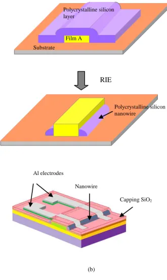
The key fabrication steps of the polycristalline silicon NWS are illustrated in figure 1 (a). At first, a dielectric film A is deposited and patterned into islands by conventional UV lithography. Then, a polycristalline silicon layer is deposited by LPCVD technique. Accurate control of the polycristalline silicon layer reactive ion etching (RIE) rate leads to the formation of nanometric size sidewall spacers that can be used as nanowires. The feasibility of these polyscristalline silicon NWs with curvature radius as low as 50 nm was previously demonstrated [21]. This method allows the fabrication of parallel SiNWs network.
Phosphorus (or Boron) in-situ doped polycrystalline silicon layers used for such nanowires were deposited by thermal decomposition of a mixture of pure silane, SiH4, and
phosphine, PH3, (or diborane, B2H6). The in-situ doping level
is controlled by adjusting the PH3/SiH4 (or B2H6/SiH4) mole
ratio varying from 0 for undoped films to 4×10⁻⁴ (or 5×10⁻⁴) for heavily doped films. Silicon films were deposited in an amorphous state at 550°C and 90 Pa, and then crystallized by a thermal annealing in vacuum at 600°C during 12 hours. The corresponding incorporated phosphorus (boron) atoms concentrations, CP (CB), previously determined from SIMS
(Secondary Ions Mass Spectroscopy) analysis, varies from 2×10¹⁶ to 2×1020 cm-3 (or 2×10¹⁶ to 5×1019 cm-3) [22]. Such results stand as reference for doping concentration in our processed SiNWs, because SIMS analysis on single nanowires is unfortunately not easy to implement.
The in-situ doped polycristalline silicon NWs were integrated into resistors devices in coplanar structure (fig. 1 (b)) for electrical characterization. In this way, the nanowires were capped by a (100nm thick) SiO2 layer deposited by
Atmospheric Pressure Chemical Vapor Deposition (APCVD) technique at 420°C and contact openings wet etched. Contacts electrodes were made of thermally evaporated aluminium and defined by wet etching. Finally a thermal annealing in forming gas (N2/H2:0.9) was carried out at 390°C to ensure good
electrical contacts. Resistors were fabricated with 10 m length parallel SiNWs.
Electrical resistivities, n and p, of N- and P-type doped
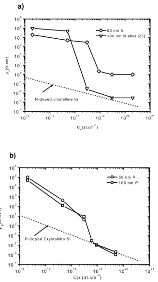
polycrystalline silicon NWS respectively were deduced from the I-V characteristics (slope) of polycrystalline silicon NWs based resistors, collected at room temperature using a HP 4155 B semiconductor parameter analyzer. The in-situ doping effect is studied through the dependence of the resistivity with the doping concentration for two different radius curvature (50 and 100nm). As shown in figures 2 (a) and (b), doping effect is different with phophorus or boron doping species.
A first partial study, previously reported by our group [23] on the N-type in-situ doping control on high curvature radius (100nm) polycrystalline silicon NWs, showed that the resistivity increasing the doping level from about 1× 1018 cm-3 results in an abrupt resistivity drop of about 6 orders of magnitude for only a factor of 10 further increase in doping concentration. Beyond that range resistivity decreases to reach the same value as for crystalline silicon. For N-type polycrystalline silicon NWs with 50nm curvature radius similar behaviour is observed, with a lower magnitude for the abrupt resistivity drop at higher doping concentrations, and higher resistivity values at high doping levels. However, the shape of these two corresponding curves, quite similar to previously observed results for in-situ doped polycrystalline silicon layers [22, 24], indicates that polycrystalline silicon NWs doping effect is in accordance with the Seto’s theory [25], in particular for high curvature radius. These results can be related to the spatial defect distribution related to the curvature radius of the polycrystalline silicon NWs. Indeed, two types of defects can be involved either located i) at the surface of the wire and/or ii) in the core of the polysilicon layer. In this last case, because the amorphous silicon crystallization process begins at the dielectric film A/amorphous silicon interface, the defects density (including grain boundaries) is higher in the inferior part of the polycrystalline silicon layer (few nanometers thick) constituting the nanowires (see figure 3). This grain morphology and defect density were previously revealed by electron microscopy study [26].
According to Seto’s theory [25], carriers transport is controlled by energy barriers induced by the trapping effect of carriers at defects located at grain boundaries. However, for lowest curvature radius (50nm) polycrystalline silicon NWs, this conduction mechanism is not dominant. Indeed, as illustrated in figure 3, grain boundaries as well as intra-grain defects densities are higher, and it is more realistic to consider structural quality quite similar to (amorphous-type or) highly disordered silicon material. Therefore, one can consider that defect density is uniformly distributed in the core of the polycrystalline silicon NWs. In this case, a more appropriate carriers transport is the variable range hopping of carriers [27]. In this model, firstly described by Mott [28], hopping refers to carriers tunneling transitions from occupied to unoccupied localized states, the state energy difference being bridged by
emission of absorption of one or several phonons.
For P-doped polycrystalline silicon NWs, the size of the nanowires does not influence the dependence of the electrical resistivity with doping concentration (fig. 2(b)): for both the electrical resistivity decreases with the increase of the doping concentration. In addition, the similar doping level dependence as for N-doped polycrystalline silicon NWs is not so evident, in particular with a slight resistivity drop region. This behaviour agrees with results previously observed for boron situ doped polycrystalline silicon layers [22]. In fact, the in-situ doping effect of boron is different from the phosphorus, and depends on the pressure deposition. Indeed, similar p
dependence with CP, as for in-situ N-doped polycrystalline
silicon layer, was observed for P-doped polysilicon layer deposited at lower deposition pressure (30Pa) [22]. This phenomenon is not well clarified for thin film polycrystalline silicon layers, and thus for polycrystalline silicon NWs. However, another study reported that for the 50nm curvature radius in-situ boron doped polycrystalline silicon NWs carriers transport follows variable range hopping mechanism [27]. Our results highlight the good control of the doping level on low curvature radius (100nm) polycrystalline silicon NWs over a wide range. The polycrystalline SiNWs gas (ammonia) sensitivity was studied using resistors based on uncapped undoped polycrystalline silicon NWs used as gas sensors. Electrical resistance (R=V/I) measurements, deduced from the slope of the linear I-V curves, are reported as function of time for devices under exposure to ammonia. Prior to measurements, devices were submitted to high diluted hydrofluoridric acid (2 %) aqueous solution to remove the native oxide on the SiNWs surface in order to promote chemical species adsorption. The electrical measurements were carried out at room temperature in nitrogen with a protocol described as follow. At first, SiNWs based devices were put into a vacuum chamber for 2 hours (P=10-4mbar). Prior ammonia injection nitrogen gas injected during few minutes to guarantee baseline leveled off. Then, the sensor was exposed to ammonia until realizing the onset of sensor response saturation. Flow and gas pressure dependences were monitored, and arbitrary ammonia pressure in the chamber during SiNWs based resistors exposure is about 500mbar. The potential use of polycrystalline SiNWs as sensitive units to ammonia was checked by measuring the detector response, Sg,
defined as: I I -I Sg g (1) (1)
where (I) and (Ig) are the current values for devices in nitrogen
and reactive ambient respectively.
The chemical responses of these SiNWs based resistors to ammonia exposure are presented in function of exposure time in figure 4. Measurements are carried out with 50 parallel (100nm radius curvature) SiNWs based devices. Upon exposure to ammonia tests, time dependence change of the electrical resistance is found to indicate a quasi reversible trend because of the recovery baseline leveled off, suggesting
that polycrystalline SiNWs could be reusable after exposure. Electrical current increases because ammonia species act as donor of electrons (reducing agents) at the SiNWs surface [29]. This behavior was previously observed [30] for such polyscristalline SiNWs based resistors under ammonia exposure. In this case, after evacuating the vacuum chamber, diluted ammonia into nitrogen is injected under controlled concentrations (700, 350, and 175 ppm) and shows that the detector response Sg increase is proportional to the increase of
the ammonia concentration. These first quantitative results, acting as proof of concept, show the potential use of polycristalline SiNWs as gas (ammonia) sensitive units. However, further studies concerning sensitivity, low detection limits, and reproducibility are needed for gas sensors applications.
Such results are explained because the gas molecules adsorption occurs at the SiNWs surface, electrons are transferred to the polycrystalline silicon SiNWs core. Such interactions induce significant changes in the carriers transport along the nanowires and SiNWs electrical resistance (or current) in different possible cumulative ways. First, as the SiNWs conductance can be modulated by an applied voltage [29,31], positively charged gas molecules (electron donors) binded on SiNWs surface can modulate their conductance by changing the volume of the conductive layer. In this case, ammonia may act as chemical gates. In other words, it means that the Fermi level of the silicon nanowires is shifted to the conduction band edge reducing the sample electrical resistance. Moreover, carrier transport strongly depends on structural nanowires defects. So, we have to consider effects of grain boundaries. Through charge exchange, gas molecules adsorbed may play a significant role in decreasing the potential barrier height at the grain boundaries between two grains. Previous work reported such effect [32]. In this case, adsorbed gas molecules passivate defects like dangling bonds leading to an increase of current [33]. The electrical current increase under ammonia exposure suggests that electrons transfer and potential barriers lowering effects may dominate. Such results act as proof of concept and show the potential usefulness of the polycrystalline silicon nanowires for high sensitive gas sensors applications operating at room temperature.
N- and P-channel Thin Film Transistors (TFTs) are fabricated using undoped polycristalline silicon NWs following the synthesis method described previously. In addition, two types of TFTs are studied: back gate and top gate devices (fig. 5). For back gate transistors the substrate is heavily doped crystalline silicon wafer acting as gate electrode (see fig. 5 (a)). The film A acting as gate insulator is a 100 nm thick Si3N4 layer deposited by LPCVD technique at 600°C. Source
and drain regions are made of heavily in-situ N-type (P-type) doped polycrystalline silicon layer deposited by LPCVD technique for N- and P-channel transistors respectively. This layer is patterned by reactive ion etching with SF6 plasma
before thermal evaporation of aluminum used for source and drain electrodes. For the top gate TFT (fig. 5 (b)), the (100nm
heavily in-situ doped polycrystalline silicon Source/Drain regions plasma patterning, and wet etched for opening contacts. Gate electrode is patterned with source and drain electrodes.
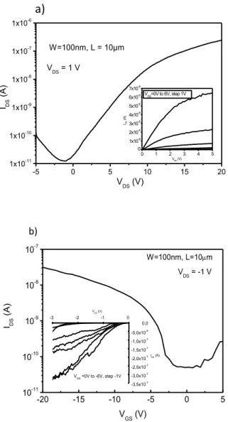
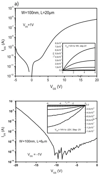
Transfer and output characteristics are displayed on the figures 6 and 7 for the two types 100nm radius curvature polysilicon NWs TFTs. Electrical parameters, threshold voltage, VT, and
optimum field effect mobility, , are determined according to the classical conduction electrical model used for the MOSFET (Metal Oxide Semiconductor Field Effect Transistor) [34]. is deduced from the maximum slope of the IDS(VGS) curve (transconductance) measured in the saturation
mode, and VT is determined by the intercept of the IDS1/2(VGS)
curve with the gate axis voltage. Switching ratio is defined as maximum (On state) to minimum (Off state) currents ratio. Average values of electrical parameters summarized in the table 1 show better electrical properties for the top gate polycrystalline silicon NWs TFTs, with a higher switching ratio and field effect mobility, and lower threshold voltage. These results are explained to the better gate insulator/polycrystalline silicon NW interface quality. Indeed, as illustrated in the figure 3, for the back gate TFTs channel region takes place in the seed layer with a higher defects density than the upper polycrystalline silicon NW surface [26]. In addition, such defects result to a poor the electrode/channel interface quality responsible of parasitic contact resistances because of the possible non linear behavior of drain current at low source-drain voltages. A lowering of the electrical properties was also observed for polycrystalline silicon NWs TFTs made with lower curvature radius polysilicon NWs, due to a higher defects density [35].
Polycrystalline SiNWs based TFTs show lower electrical properties than for those based on polycrystalline silicon layer. However, our study shows that back gate TFT could be used as sensitive blocks because in this configuration polycrystalline silicon NW can be submitted to charged species ambient, and thus the field effect could be promising to amplify chemical species detection. Thanks to their promising electrical properties, top gate transistors are potential candidates for electronics conditioning sensing signal.
IV. CONCLUSION
Our study shows the great flexibility in design of planar SiNWs array by direct patterning technique using conventional lithographic tools. The N- and P-type polycrystalline silicon NWs doping control make them good candidates for the fabrication of electrically controlled thin film devices (resistors and transistors), in particularly for specific gas (reducing) sensing or electronics applications.
Results show the full compatibility of the nanospacer polysilicon nanowires technology with the existing silicon CMOS technology, using nanowires as potential sensitive units
transistors is promising to amplify chemical species detection as well as for electronics conditioning sensing signal for back gate and top gate configurations respectively.
In addition, thanks to silicon surface functionalization possibilities, such results offer a great potential for further developments of integrated SiNWs based (bio)chemical sensors and their implementation in electronic systems.
ACKNOWLEDGMENTS
This work was supported by the Agence Nationale de la Recherche (France) with the Project Sena (ANR-09JCJC-0072-01).
REFERENCES
[1] J. Goldberger, A. I. Hochbaum, and R. Fan, P Yang, “Silicon Vertically Integrated Nanowire Field Effect Transistors”, Nanoletters, 6(5) (2006) 973
[2] C. Yang, C. J. Barrelet, F. Capasso, and C.M. Lieber, “Single p-Type/Intrinsic/n-Type Silicon Nanowires as Nanoscale Avalanche Photodetectors”, Nanoletters, 6(12) (2006) 2929
[3] Y. Cui, Q. Wei, H. K. Park, and C. M. Lieber, “Nanowire nanosensors for highly sensitive and selective detection of biological and chemical species”, Science, 293(5533) (2001) 1289.
[4] Z. Li, Y. Chen, X. Li, T.I. Kamins, K. Nauka, and R. S. Williams,
“Sequence-specific label-free DNA sensors based on silicon nanowires”,
Nanoletters, 4(2) (2004) 245
[5] H. J. In, C. R. Field, P. E. Pehrsson , “Periodically porous top electrodes
on vertical nanowire arrays for highly sensitive gas detection”,
Nanotechnology, 22, 355501 (2011)
[6] M.C. McAlpine, H. Ahmad, D. Wang, J. R. Heath, “Highly ordered nanowires arrays on plastic substrates for ultrasensitive flexible
chemical sensors” , Nature Materials, 5, 379 (2007)
[7] M. Cuscuna, A. Convertino, E. Zampetti, A. Macagnano, A. Pecora, G.
Fortunato, L. Felisari, G. Nicotra, C. Spinella, F. Martelli, “On-chip
fabrication of ultrasensitive NO2sensors based on silicon nanowires”,
Appl. Phys. Lett. 101, 103101 (2012)
[8] Liu Y and Cui T, “Silica nanowires fabricated with layer-by-layer self-assembled nanoparticles”, J Nanosci. Nanotechnol, 6(4) (2006) 1019. [9] P. Cheyssac, M. Sacilotti, and G. Patriarche, “Vapor-liquid-solid
mechanisms: Challenges for nanosized quantum cluster/dot/wire materials”, J. Appl. Phys. 100, (2006) 044315
[10] L.Yu. and P Roca i Cabarrocas, “Growth mechanism and dynamics of in-plane solid-liquid-solid silicon nanowires”, Physical Review B 81, (2010) 085323
[11] I. Michelakaki, A. G. Nassiopoulou, E. Stavrinidou, K. Breza, and N. Frangis, “Porous anodic alumina on galvanically grown PtSi layer for application in template-assisted Si nanowire growth”, Nanoscale
Research Letters, 6 (2011) 414
[12] H. Xiang-Lei, L. Guilhem, F. Pier-Francesco, and D. Emmanuel,
Microelectr. Eng., 88 (8) (2011) 2622
[13] I. Ionica, L. Montes, S. Ferraton, J. Zimmermann, L. Saminadayar, and V. Bouchiat, “Field effect and colomb blockage in silicon on insulator nanostructures fabricated by atomic force microscope”, Solid State
Electronics, 49 (2005) 1497
[14] L Pichon, R Rogel, and F Demami, “Fabrication of amorphous silicon nanoribbons by atomic force microscope tip-induced local oxidation for thin film device applications”, Semicond. Sci. Technol. 25 (2010) 065001
[15] L. Yang, D. H. Lee, Y. H. Chen, C. Y. Chang, S. D. Liu, and C. C. Huang, VLSI Symp. Tech. Dig, (2004) 196
[16] S.Y. Chou, R. Krauss, and P. J. Renstrom, “Nanoscale silicon field effect transistors fabricated using imprint lithography”, Science, 85 (1996) 272
[17] A. Talin, L. Hunter, F. Léonard, and B. Rokad, “Large area dense silicon nanowire array chemical sensors”, Applied Physics Letters 89 (2006), 153102.
[18] M. Lee, Y. Jeon, T. Moon, S. Kim, “Top-Down Fabrication of Fully CMOS-Compatible Silicon Nanowire Arrays and Their Integration into
CMOS Inverters on Plastic” ACS NANO, 5(4), 2629 (2011)
[19] K. D. Buddharaju, N. Singh, S. C. Rustagi, S. H.G. Teo, G. Q. Lo, N. Balasubramanian, D. L. Kwong, “Si-nanowire CMOS inverter logic fabricated using gate-all-around (GAA) devices and top-down
approach” Sol. St. Elect. 52, 1312 (2008)
[20] F. Wessely, T. Krauss, U. Schwalke,“CMOS without doping: multi-gate silicon-nanowire fiel effect transistors“, Sol. St. Elect. 70, 33 (2012) [21] F. Demami, L. Pichon, R. Rogel, and A. C. Salaun, “Fabrication and
electrical characterization of silicon nanowires based resistors”, Mat. Sc.
Eng. , 012014 (2009)
[22] D. Briand, M. Sarret, F. Le Bihan, O. Bonnaud, and L. Pichon,
“Polysilicon phosphorus doping control over large concentration range
using low temperature, low pressure chemical vapour deposition growth process”, Mat. Sci. Tech. 11 1207 (1995)
[23] F. Demami, R. Rogel, A. C. Salaun, L. Pichon, “Electrical properties of polysilicon nanowires for devices applications”, Phys. Stat. Sol. 8(3),
827 (2011)
[24] D. Briand, Ph Dissertation, “Silicium déposé par LPCVD et dopé in-situ: dépôt, caractérisation et application », Université de Rennes 1, France (1995)
[25] J. W. Seto, “The electrical properties of polycristalline silicon films”, J.
Appl. Phys. 46, 5247 (1975)
[26] L. Haji, P. Joubert, J. Stoemenos, N. A. Economou, “Mode of growth and microstructure of polycrystalline silicon obtained by solid phase
crystallization of an amorphous silicon film”, J. Appl. Phys. 75(8), 3944
(1994)
[27] L. Pichon, E. Jacques, R. Rogel, A. C. Salaun, and F. Demami,
“Variable range hopping mechanism in N- and P-type in-situ doped
polycristalline silicon nanowires”, Semicond. Sc. Tech.28, 025002 (2013)
[28] N. F. Mott, “Conduction in non-crystalline materials III. Localized states in a pseudogap and near extremities of conduction and valence bands”,
Philos. Mag. 19, 835 (1969)
[29] A. A. Talin, L. L. Hunter, F. Leonard, and B. Rokad, “Large area, dense silicon nanowire array chemical sensors”, Appl. Phys. Lett, 89 (2006)153102
[30] F. Demami, L. Ni, R. Rogel, A. C. Salaun, L. Pichon,”Silicon nanowires
based resistors as gas sensors”, Sensors and Actuators B, 170, 158
(2012)
[31] J. Y. Yu, S. W. Chung, and J. R. Heath, “Silicon naowires: preparation, device fabrication, and transport properties”, J. Phys. Chem, B 104, 11864 (2000).
[32] Y. Shimizu and M. Eg-ashira, “Basic aspects and challenges of semiconductor gas sensors”, MRS Bull, (June) pp. 18-24 (1999). [33] N.K. Ali, M.R. Hashim, and A. Abdul Aziz, “Effects of surface
passivation in porous silicon as H2 gas sensor”, Sol. St. Elect., 52, 1017 (2008)
[34] S. M. Sze, “Physics of semiconductor devices”, 2nd edition (Wiley), p 442 (1981)
[35] F. Demami, “Synthèse de nanofils de silicium par la méthode des espaceurs pour dispositifs électroniques », Ph Dissertation, université de Rennes1, France (2011)
(b)
Figure 1. Fabrication of polycrystalline silicon NWs by the sidewall spacer formation technique (a). Polycristalline silicon nanowires based resistor for electrical characterization (b) Nanowire Capping SiO2 Al electrodes Polycrystalline silicon nanowire Film A Substrate Polycrystalline silicon layer RIE
Figure 2. Electrical resistivities of (50nm and 100nm curvature radius) polycrystalline SiNWs variations versus phosphorus (a), boron (b) concentration.
Figure 3: Schematic cross section view illustrating the columnar type structure of a polycristalline silicon layer: size lowering leads to a higher defects density within the polycristalline SiNWs.
0,0 3,0x10³ 6,0x10³ 2,0x10⁻¹⁰ 4,0x10⁻¹⁰ 6,0x10⁻¹⁰ 8,0x10⁻¹⁰ 1,0x10⁻⁹ 1,2x10⁻⁹ P=500mbar R/R=660% R/R=1200% I (A) Time (s) 700 ppm 350 ppm 175 ppm 1 1 : under N 2 flow 2 : under NH3/N2 flow 3 : under N2 flow 2 2 2 3 3 3 R/R=2160%
Figure 4. Variations of the current versus time under controlled ammonia exposure. The pressure adjusted in the chamber is 500 mbar, and measurements are carried out at room temperature. SiNWs radius curvature: 100nm 100 nm 50 nm Seed layer 1 01 6 1 01 7 1 01 8 1 01 9 1 02 0 1 02 1 1 0-4 1 0-3 1 0-2 1 0-1 1 00 1 01 1 02 1 03 1 04 1 05 1 0 N -d o p e d c rys ta llin e S i n ( .c m ) C n(a t.c m -3 ) 5 0 n m N 1 0 0 n m N a fte r [2 3 ] 1 01 6 1 01 7 1 01 8 1 01 9 1 02 0 1 02 1 1 0-4 1 0-3 1 0-2 1 0-1 1 00 1 01 1 02 1 03 1 04 1 05 1 06 P -d o p e d C rys ta llin e S i p ( .c m ) C p (a t.c m-3) 5 0 n m P 1 0 0 n m P b)
Figure 5: Back gate (a) and Top gate (b) polycristalline SiNWs based TFTs.
Figure 6. Transfer electrical characteristics of N-channel (a), P-channel (b) back gate polycristalline SiNWS based TFTs. Inserts output electrical characteristics. Source Drain Gate capping layer b) capping layer Drain Source Gate
(highly doped Si mono)
a) -5 0 5 10 15 20 1x10-11 1x10⁻¹⁰ 1x10⁻⁹ 1x10⁻⁸ 1x10⁻⁷ 1x10⁻⁶ 0 1 2 3 4 5 0 1x10⁻⁹ 2x10⁻⁹ 3x10⁻⁹ 4x10⁻⁹ 5x10⁻⁹ 6x10⁻⁹ 7x10⁻⁹ IDS ( A ) VDS (V) VGS=0V to 6V, step 1V IDS (A) VDS (V) W=100nm, L = 10µm VDS = 1 V
a)
-20 -15 -10 -5 0 5 10-11 10-10 10-9 10-8 10-7 -3 -2 -1 0 -3,5x10⁻⁷ -3,0x10⁻⁷ -2,5x10⁻⁷ -2,0x10⁻⁷ -1,5x10⁻⁷ -1,0x10⁻⁷ -5,0x10⁻⁸ 0,0 V GS =0V to -6V, step -1V VDS (V) IDS (A) IDS (A) VGS (V) VDS = -1 V W=100nm, L=10m b)-5 0 5 10 15 20 10-12 10-11 10-10 10-9 10-8 10-7 10-6 10-5 0 2 4 6 0,0 1,0x10⁻⁷ 2,0x10⁻⁷ 3,0x10⁻⁷ 4,0x10⁻⁷ 5,0x10⁻⁷ 6,0x10⁻⁷ 7,0x10⁻⁷ 8,0x10⁻⁷ IDS ( A ) VDS (V) VGS=12V to 18V, step 2V W=100nm, L=20µm IDS (A) VGS (V) VDS=1V -20 -15 -10 -5 0 10-14 10-13 10-12 10-11 10-10 10-9 10-8 IDS (A) VGS (V) VDS = -1V W=100nm, L=6m -6 -4 -2 0 -1,4x10⁻⁷ -1,2x10⁻⁷ -1,0x10⁻⁷ -8,0x10⁻⁸ -6,0x10⁻⁸ -4,0x10⁻⁸ -2,0x10⁻⁸ 0,0 VDS (V) VGS=-14V to -22V, Step -2V IDS (A)
Figure 7. Transfer electrical characteristics of N-channel (a), P-channel (b) top gate polycristalline SiNWS based TFTs. Inserts output electrical characteristics.
TABLE 1.SUMMARY OF THE ELECTRICAL PARAMETERS (AVERAGE VALUES) OF THE BACK AND TOP GATE TFTS MADE OF 100NM CURVATURE RADIUS POLYCRISTALLINE SILICON NWS.
Top Gate Back Gate
N-channel P-channel N-channel* P-channel
(cm2 /Vs) 30 12 3 < 3 VT (V) 7 - 16 7 - 8 Switching ratio 106 ~ 107 ~ 104 >103
* Results for back gate N-Channel polycristallin SiNWs based transistors were previously reported in the ref [23]
R. Rogel received the Ph.D. degree in electronics from the université de Rennes 1, France, in 2001. He is currently with the Institut d’Electronique et des Télécommunications de Rennes, France. His main research interests include electrical characterization of silicon nanowires based devices for sensor or electronics applications..
E. Jacques is assistant professor. He received his PhD degree in Electronic
from the institute d’Electronique et Télécommunications of Rennes (IETR) in
2008. His research interest covers the technological process optimization of low temperature electronic devices, the study of polysilicon nanowires made for sensors applications and electronic devices, and he also worked on display fabrication, especially in addressing matrix system made of microcrystalline silicon on flexible substrate.
L. Pichon received his Ph D degree in physics from the university of Rennes (France) in 1993, and his Habilitation à Diriger des Recherches in electronics from the university of Caen (France) in 2001. From 1996 to 2005 he was associate professor at the university of Caen. His research activities were focused on the low temperature (<600°C) polysilicon TFT fabrication and electrical characterization by low frequency noise measurements. Since 2005
he is professor at the “Departement Microelectronique et Microscapteurs” (DM2) of the Institut d’Electronique et des Télécommunications de Rennes
(IETR) university of Rennes. His research are focused on silicon nanowires technology for CMOS electronics and senors applications. Since 2012 he is
the menanger of the “Composants Microelectroniques” team of the
DM2-IETR, including 3 professors, 4 associate professors, 1 research engineer, 1 post doctorate and 5 phD students. He is author and co-author of 70 international papers published in reviews or conference proceedings. A.C. Salaün was born in Rennes, France, in 1970. She received the Docteur-es-science Physique degree in 1996 from the University of Rennes, France.
She is associate professor since 1998 in the Institut d’Electronique et de
Telecommunications de Rennes (IETR). Her activity is devoted to the micro-technology, with applications to chemical and biological sensors. She is author or co-author of 45 international papers or conference proceedings.