HAL Id: hal-01736097
https://hal.archives-ouvertes.fr/hal-01736097
Submitted on 27 Mar 2018
HAL is a multi-disciplinary open access
archive for the deposit and dissemination of
sci-entific research documents, whether they are
pub-lished or not. The documents may come from
teaching and research institutions in France or
abroad, or from public or private research centers.
L’archive ouverte pluridisciplinaire HAL, est
destinée au dépôt et à la diffusion de documents
scientifiques de niveau recherche, publiés ou non,
émanant des établissements d’enseignement et de
recherche français ou étrangers, des laboratoires
publics ou privés.
Multi-dot floating-gates for nonvolatile semiconductor
memories: Their ion beam synthesis and morphology
T. Müller, K.-H. Heinig, W. Möller, Caroline Bonafos, H. Coffin, Nikolay
Cherkashin, Gérard Benassayag, Sylvie Schamm-Chardon, G. Zanchi, Alain
Claverie, et al.
To cite this version:
T. Müller, K.-H. Heinig, W. Möller, Caroline Bonafos, H. Coffin, et al.. Multi-dot floating-gates for
nonvolatile semiconductor memories: Their ion beam synthesis and morphology. Applied Physics
Letters, American Institute of Physics, 2004, 85 (12), pp.2373-2375. �hal-01736097�
Multi-dot floating-gates for nonvolatile semiconductor memories: Their ion beam
synthesis and morphology
T. Müller, K.-H. Heinig, W. Möller, C. Bonafos, H. Coffin, N. Cherkashin, G. Ben Assayag, S. Schamm, G. Zanchi, A. Claverie, M. Tencé, and C. Colliex
Citation: Appl. Phys. Lett. 85, 2373 (2004); doi: 10.1063/1.1794856 View online: https://doi.org/10.1063/1.1794856
View Table of Contents: http://aip.scitation.org/toc/apl/85/12 Published by the American Institute of Physics
Articles you may be interested in
Size and location control of Si nanocrystals at ion beam synthesis in thin films Applied Physics Letters 81, 3049 (2002); 10.1063/1.1512952
Sponge-like Si-SiO2 nanocomposite—Morphology studies of spinodally decomposed silicon-rich oxide Applied Physics Letters 103, 131911 (2013); 10.1063/1.4820453
Formation and coarsening of sponge-like Si-SiO2 nanocomposites Applied Physics Letters 103, 133106 (2013); 10.1063/1.4822125
Manipulation of two-dimensional arrays of Si nanocrystals embedded in thin layers by low energy ion implantation
Journal of Applied Physics 95, 5696 (2004); 10.1063/1.1695594
Stress measurements of germanium nanocrystals embedded in silicon oxide Journal of Applied Physics 94, 5639 (2003); 10.1063/1.1617361
Layer morphology and implant profiles after annealing of supersaturated, single-crystalline, amorphous, and nanocrystalline
Multi-dot floating-gates for nonvolatile semiconductor memories: Their ion
beam synthesis and morphology
T. Müller,a)K.-H. Heinig, and W. Möller
Research Center Rossendorf, Institute of Ion Beam Physics and Materials Research, P.O. Box 51 01 19, 01314 Dresden, Germany
C. Bonafos, H. Coffin, N. Cherkashin,b) G. Ben Assayag, S. Schamm, G. Zanchi, and A. Claverie
nMat Group, CNRS/CEMES, 29 Rue Jeanne Marvig, 31055 Toulouse, France
M. Tencé and C. Colliex
Laboratoire de Physique des Solides, Université Paris-Sud-UMR 8502, 91405 Orsay, France (Received 9 February 2004; accepted 20 July 2004)
Scalability and performance of current flash memories can be improved substantially by replacing the floating polycrystalline-silicon gate by a layer of Si dots. Here, we present both experimental and theoretical studies on ion beam synthesis of multi-dot layers consisting of Si nanocrystals (NCs) embedded in the gate oxide. Former studies have suffered from the weak Z contrast between Si and SiO2 in transmission electron microscopy (TEM). This letter maps Si plasmon losses with a
scanning TEM equipped with a parallel electron energy loss spectroscopy system. Kinetic Monte Carlo simulations of Si phase separation have been performed and compared with Si plasmon maps. Predicted and measured Si morphologies agree remarkably well, both change with increasing ion fluence from isolated NCs to spinodal pattern. However, the predicted fluences are lower than the experimental ones. We identify as the main reason of this discrepancy the partial oxidation of implanted Si by atmospheric humidity, which penetrates into the as-implanted SiO2. © 2004
American Institute of Physics. [DOI: 10.1063/1.1794856]
Metal-oxide-silicon field-effect transistors with an elec-trically isolated(“floating”) gate layer embedded in the gate oxide are currently used as flash memories. The replacement of this floating-gate by a layer of discrete Si nanocrystals (NCs)1
improves the performance of flash memories substantially.2 The reduced probability for a complete dis-charging of the multi-dot floating-gate by oxide defects al-lows thinner tunnel oxides. In turn, the floating-gate will be charged/discharged by quantum mechanical direct electron tunneling (instead of defect-generating Fowler–Nordheim tunneling). The memory operation voltage can be reduced and scalability is improved. Using ion beam synthesis, the multi-dot floating-gate can be fabricated along with standard (CMOS) processing.3
Si+ions are implanted at ultralow
en-ergies into the gate oxide, causing there a high Si ration. During postimplantation annealing, this Si supersatu-ration leads to phase sepasupersatu-ration of elemental Si from SiO2.
4
Imaging this phase separation process is difficult. Transmis-sion electron microscopy (TEM) has historically suffered from weak Z contrast between Si and SiO2phases. Recently,
this problem was partially overcome by Fresnel imaging us-ing under-focused bright field conditions.5Thus, the distance of the layer of phase separated Si from the transistor channel could be determined.6,7 However, this technique fails to re-solve the morphology of the phase separated Si. For instance, recent kinetic Monte Carlo (KMC) simulations of phase separation predict a pronounced fluence dependence of the precipitate morphology.4For low Si+fluences, spherical and
isolated Si NCs form by nucleation and growth, while for
higher Si+fluences spinodal decomposition occurs. The elon-gated, non-spherical Si structures, formed by spinodal de-composition, coalesce at even higher fluences to an intercon-nected, labyrinthine Si network. This letter uses a scanning TEM(STEM) with an efficient parallel electron energy loss spectroscopy(PEELS) system, to confirm the predictions of the KMC simulations. The contrast problem of conventional TEM could be overcome by mapping Si plasmon losses, which differ from SiO2. Comprehensive KMC studies and
PEELS-STEM analysis has been performed to understand the complex process of phase separation in a thin buried layer.
To form Si NCs by phase separation, Si+ions have been
implanted at 1 keV energy into 10-nm-thick SiO2 layers,
which were thermally grown on(001) Si substrates. Using an AXCELIS GSD-ULTRA ultralow-energy implanter, fluences of 5⫻1015, 1⫻1016, and 2⫻1016cm−2 were implanted at
room temperature. Surface charging due to implantation was compensated by a Xe plasma electron flood gun. The im-planted samples were cleaned using a piranha solution and furnace annealed for 30 min in N2 at 950 °C. From all
samples, cross sectional and plane view TEM specimens were prepared by the standard procedure of grinding, dim-pling, and Ar+ ion beam thinning. PEELS-STEM was per-formed on plane view samples using a scanning TEM VG-HB 501 operating at 100 kV that is equipped with a field emission cathode and a parallel Gatan 666 EELS spectrom-eter. Low-loss EELS spectra were recorded at each picture point, hence a spectrum image was acquired.8These spectra were fitted in the energy range of 15–30 eV by a weighted sum of two plasmon reference spectra, which were obtained from bulk Si and SiO2. Potential size effects like shifts of the Si plasmon resonance of small Si NCs were not
compen-a)Electronic mail: [email protected]
b)On leave from: Ioffe Physico-Technical Institute, St. Petersburg.
APPLIED PHYSICS LETTERS VOLUME 85, NUMBER 12 20 SEPTEMBER 2004
sated. The gray level of the PEELS-STEM image pixels is given by the ratio of the intensity of the Si plasmon peak and the total intensity of the Si and SiO2 plasmon peaks and,
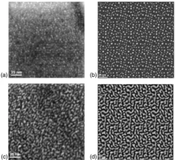
therefore, maps the Si bulk plasmons. Quantitative Si con-centrations, however, cannot be given, only the relative Si content is imaged. In Fig. 1, such Si plasmon maps(on the left-hand side) are compared to plane view snapshots of KMC simulations (on the right-hand side). This atomistic approach to phase separation of excess Si in thin SiO2layers
by atomistic simulations was recently described in detail in Refs. 4 and 9. The depth profiles of excess Si due to high fluence Si+ion implantation into thin gate oxides have been calculated by the binary collision programTRIDYN10 account-ing for the effects of ion erosion, target swellaccount-ing, and ion beam mixing dynamically. The postimplantation phase sepa-ration during thermal treatment is described by a kinetic three-dimensional lattice Monte Carlo program package.11,12 Taking theTRIDYN profiles of Si excess as well as Si solu-bility and diffusivity in SiO2as input, the program describes
excess Si diffusion, precipitation, and Ostwald ripening in the thin SiO2 layer under the constraints of the boundary
conditions of a nearby Si/ SiO2 interface and a free SiO2
surface. Here, we use a simplified version of the KMC pro-gram, i.e., only Ising-type nearest-neighbor interactions. It should be noted that KMC simulations with measured Si self-diffusivities13,14lead to too long annealing times or too high temperatures. Obviously, the diffusive Si mass transport by a mobile SiO2 defect with local Si excess (that could
either be named Si interstitial, SiO molecule,13 or oxygen vacancy15) does not necessarily follow the same mechanism as the 28SiO2/30SiO2 interface broadening, which was ana-lyzed in self-diffusivity studies. In this letter, the discrepancy between diffusive Si mass transport and Si self-diffusivity will not be discussed as our theoretical predictions aim at the reaction pathway of SiOx decomposition rather than at a
quantitative prediction of annealing time and temperature.
Thus, KMC simulations utilize a relative time scale ”Monte Carlo steps”(MCS) that allows a posterior recalibration with realistic Si diffusivities.12
Image processing of KMC simulation data allowed one to obtain KMC simulation snapshots that can be compared directly to PEELS-STEM or Fresnel images. In plane view, the simulation cell has been tripled laterally taking advantage of the periodic boundary conditions. The number of excess Si atoms in the vertical column below the pixel at 共x,y兲 determines its gray level. The highest occurring number of Si atoms in such a column is assigned to white, whereas black means that no Si excess is found in the SiO2matrix.
No Si precipitates were observed in the sample for the lowest Si+fluence of 5⫻1015cm−2(TEM images not shown
here). For the medium Si+ fluence of 1⫻1016cm−2, white spots in a dark background appear in the plane view Si plas-mon map shown in Fig. 1(a) indicating spherical Si NCs embedded in the SiO2 matrix. During thermal annealing,
these NCs have formed by nucleation and growth in the Si enriched region of the implanted SiO2 layer. The observed
NCs are relatively small with an estimated mean diameter of 2.7 nm and have a high area density of 3.3⫻1012cm−2. A
similar precipitate morphology with the same mean NC size and density is found in the KMC simulation snapshot of Fig. 1(b), but for a significantly lower Si+ fluence of 3
⫻1015cm−2and a KMC simulation(annealing) time of 2100
kMCS. It should be noted that even this “medium” experi-mental Si+fluence of 1⫻1016cm−2leads in the KMC
simu-lation to the formation of coalesced poly-Si layer buried in the SiO2.
4
For the highest Si+ fluence of 2⫻1016Si+cm−2,
the morphology of the phase separated Si has changed com-pletely as observed in Fig. 1(c). A spaghetti-like network of white and black regions is found. This pattern clearly indi-cates that phase separation took place by spinodal decompo-sition. Even more, percolation is observed. Si precipitates are no longer spatially isolated, but an interconnected network of phase separated Si has formed. An equivalent morphology with the same typical distances as in Fig. 1(c) between the spinodal fingers is found in the KMC simulation snapshot of Fig. 1(d). This result was obtained for 8⫻1015Si+cm−2and a
simulation time of 300 kMCS. Strikingly, the morphology agrees remarkably well between both images, while simula-tion snapshots for other fluences or annealing times deviate instead considerably from the morphology seen in Fig. 1(c). Samples were studied additionally in cross section using a CM30 Phillips TEM equipped with a LaB6 cathode oper-ating at 300 kV. Fresnel imaging conditions were applied in order to achieve at least a weak contrast between Si and SiO2
in cross sectional TEM (XTEM) images,5i.e., images were taken at out-of-Bragg alignment and under strongly underfo-cused bright field conditions. Details of the responsible con-trast mechanism are given in Ref. 5. Figures 2(a) and 2(c) show the XTEM Fresnel images for fluences of 1 ⫻1016Si+cm−2 and 2⫻1016Si+cm−2, respectively. Cross
section KMC simulation snapshots are displayed in Figs. 2(b) and 2(d) for 3⫻1015Si+cm−2 (2100 kMCS) and 8
⫻1015Si+cm−2 (300 kMCS), respectively. Thereby, plane
view image processing was applied to KMC cross section views with an inverted gray scale. In all images, the phase separated Si forms a single, sharp layer seen as gray band in the SiO2 that is well separated from the SiO2/ Si interface.
Due to the extremely shallow Si excess profile obtained by low-energy Si+ implantation, phase separation is
quasicon-FIG. 1. Morphology of phase separated Si in SiO2. Si plasmon maps by
PEELS-STEM (a),(c) are compared to corresponding KMC simulations (b),(d). Nucleation of Si NCs is observed (a) for a Si fluence of 1 ⫻1016cm−2and predicted with the same morphology for(b) 3⫻1015cm−2.
Spinodal patterns are imaged(c) for 2⫻1016cm−2and simulated(d) for 8
⫻1015cm−2. Bright and dark regions correspond to Si and SiO 2 phases,
respectively.
fined to two dimensions. For 1⫻1016Si+cm−2, Si precipi-tates align nicely in a thin layer, which is just a few nanom-eters thick, Fig. 2(a). When the Si+fluences are increased to
2⫻1016Si+cm−2, the precipitate layer remains comparatively well localized in depth, Fig. 2(c), although the Si morphol-ogy observed in plane view has changed completely, Fig. 1(c). The total SiO2 thickness is systematically smaller for
the KMC simulations than for the corresponding Fresnel XTEM images. Nevertheless, the distance between the Si/ SiO2 interface and the phase separated Si agrees nicely
for experiment and simulation.
The Si fluences in our KMC simulations were chosen in order to obtain morphologies of phase separated Si, which are similar to experimental ones. This adjustments of our simulation reveals a strong discrepancy between experimen-tal and theoretical Si fluences. More Si than theoretically predicted has to be implanted. Not all Si that has nominally been implanted into the SiO2 is available for phase
separa-tion. The reason for the missing Si excess might be twofold. (i) Recent time of flight secondary ion mass spectroscopy measurements on low-energy, low-fluence30Si+as-implanted SiO2samples indicate that only a fraction of about 0.5–0.7 of
the nominal Si+fluence has been implanted into the SiO2. 16
(ii) It is known that (Si or Ge) NC formation in very thin SiO2films is extremely sensitive to humidity absorbed by the
as-implanted (damaged) glass network17 as well as to oxi-dants being present in the annealing ambient.18Thus, a con-siderable amount of the implanted Si might become oxidized during annealing. This explains also why no NCs have been observed by TEM for the lowest Si+ fluence of 5
⫻1015cm−2. The implanted Si has been oxidized completely
during the thermal annealing. At the same time, oxidation of the implanted Si leads to a volume expansion that increases the overall SiO2layer thickness.
6
This swelling of the SiO2
due to Si oxidation can be seen in the XTEM images of Figs. 2(a)–2(c) if compared to the KMC simulation snapshots, Figs. 2(b) and 2(d), which just include the SiO2 expansion
due to the incorporated Si atoms.9 Here, the KMC simula-tions do not account for oxidation and the swelling caused by it. To do so, a multicomponent KMC approach 共Si+O兲 is needed. Though samples have been annealed under fixed
ex-perimental conditions, the KMC simulation snapshots of cor-responding Si patterns refer to different simulation times. Two reasons might be responsible for this discrepancy in the evolution speed. At first, the oxidation of a substantial part of implanted Si might influence the kinetics, and second, the Si bulk diffusion in SiO2might differ substantially from the Si diffusion at the Si/ SiO2 interface. Studies that investigate
this point are under way.
Summarizing, extensive studies on low-energy ion beam synthesis of multi-dot Si floating-gates embedded in thin SiO2 layers have been presented. The morphology of this
floating-gate layer is imaged by PEELS-STEM. A direct comparison to kinetic three-dimensional lattice Monte Carlo simulation snapshots have been made and show a remarkable agreement between the atomistic simulations and the PEELS-STEM images. A strong fluence dependence of the precipitate morphology is confirmed. For low Si+ fluences,
isolated Si NCs form by nucleation and growth, while high fluences lead to spinodal pattern. Predicted and measured morphologies agree remarkably well. However, the predicted fluences are lower than the experimental ones. A substantial fraction of the implanted Si is lost by parasitic oxidation with atmospheric humidity.
This work was supported by the European Commission through the Growth project G5RD/2000/00320—NEON.
1
S. Tiwari, F. Rana, H. Hanafi, A. Hartstein, E. F. Crabbe, and K. Chan, Appl. Phys. Lett. 68, 1377(1996).
2
S. Tiwari, J. A. Wahl, H. Silva, F. Rana, and J. J. Welser, Appl. Phys. A: Mater. Sci. Process. 71, 403(2000).
3
E. Kapetanakis, P. Normand, D. Tsoukalas, and K. Beltsios, Appl. Phys. Lett. 80, 2794(2002).
4
T. Müller, K.-H. Heinig, and W. Möller, Appl. Phys. Lett. 81, 3049 (2002).
5
G. B. Assayag, C. Bonafos, M. Carrada, P. Normand, D. Tsoukalas, and A. Claverie, Appl. Phys. Lett. 82, 200(2003).
6
M. Carrada, N. Cherkashin, C. Bonafos, G. Benassayag, D. Chassaing, P. Normand, D. Tsoukalas, V. Soncini, and A. Claverie, Mater. Sci. Eng., B
101, 204(2003).
7
C. Bonafos, M. Carrada, N. Cherkashin, H. Coffin, D. Chassaing, G. Ben Assayag, A. Claverie, T. Müller, K. H. Heinig, M. Perego, M. Fanciulli, P. Normand, and D. Tsoukalas, J. Appl. Phys. 95, 5696(2004).
8
C. Jeanguillaume and C. Colliex, Ultramicroscopy 28, 252(1989).
9
T. Müller, K.-H. Heinig, and W. Möller, Mater. Sci. Eng., B 101/1-3, 49 (2003).
10
W. Möller, and W. Eckstein, Nucl. Instrum. Methods Phys. Res. B 2, 814 (1984).
11
K.-H. Heinig, T. Müller, B. Schmidt, M. Strobel, and W. Möller, Appl. Phys. A: Mater. Sci. Process. 77, 17(2003).
12
M. Strobel, K.-H. Heinig, and W. Möller, Phys. Rev. B 64, 245422 (2001).
13
M. Uematsu, H. Kageshima, Y. Takahashi, S. Fukatsu, K. M. Itoh, K. Shiraishi, and U. Gösele, Appl. Phys. Lett. 84, 876(2004).
14
D. Mathiot, J. P. Schunck, M. Perego, M. Fanciulli, P. Normand, C. Tsa-mis, and D. Tsoukalas, J. Appl. Phys. 94, 2136(2003).
15
J. Song, L. R. Corrales, G. Kresse, and H. Jonsson, Phys. Rev. B 64, 134102(2001).
16
M. Perego, M. Fanculli, G. Ben Assayag, and A. Claverie,(private com-munication).
17
B. Schmidt, D. Grambole, and F. Herrmann, Nucl. Instrum. Methods Phys. Res. B 191, 482(2002).
18
S. Oswald, B. Schmidt, and K.-H. Heinig, Surf. Interface Anal. 29, 249 (2000).
FIG. 2. Cross-section view of the layer of phase separated Si in SiO2.
Fresnel XTEM images for(a) 1⫻1016Si+cm−2and(c) 2⫻1016Si+cm−2are
compared to cross-sectional KMC simulation snapshots for (b) 3 ⫻1015Si+cm−2and(d) 8⫻1015Si+cm−2.