HAL Id: tel-01322448
https://tel.archives-ouvertes.fr/tel-01322448
Submitted on 6 Jul 2017
HAL is a multi-disciplinary open access
archive for the deposit and dissemination of sci-entific research documents, whether they are pub-lished or not. The documents may come from teaching and research institutions in France or
L’archive ouverte pluridisciplinaire HAL, est destinée au dépôt et à la diffusion de documents scientifiques de niveau recherche, publiés ou non, émanant des établissements d’enseignement et de recherche français ou étrangers, des laboratoires
To cite this version:
Pierre Rale. Multi-transition solar cells with localised states. Physics [physics]. Université Pierre et Marie Curie - Paris VI, 2015. English. �NNT : 2015PA066541�. �tel-01322448�
Thèse de doctorat
Discipline : physique des matériaux
Présentée par Pierre Rale
Multi-transition solar cells with
localised states
Mme Hélène Carrère INSA Toulouse Rapporteur
M. Ludovic Escoubas IM2NP Rapporteur
M. Abhay Shukla UPMC Examinateur
M. Olivier Durand INSA Rennes Examinateur
M. Yoshitaka Okada Université de Tokyo Examinateur
Acknowledgement
Je tiens à remercier Jean-François Guillemoles en premier lieu pour avoir élaboré et dirigé ma thèse. Sa grande culture scientifique et sa clairvoyance auront été d’une grande aide pour avancer pendant ces trois années. Je le remercie pour les opportunités qu’il m’a offertes d’aller dans des conférences nationales et internationales présenter mon travail, mais également pour m’avoir permis d’aller passer 3 semaines au sein du laboratoire Rcast au Japon qui auront été pleines d’enseignements pour ma fin de thèse. Vient ensuite bien évidemment Laurent Lombez, mon encadrant de thèse, qui a suivi au quotidien mon évolution. Il a joué un rôle déterminant dans le déroulement de ma thèse, notamment en me permettant d’élargir mon champ d’étude aux cellules à bandes intermédiaires au moment où mon sujet initial était à l’arrêt. Il a été mon référent scientifique et un soutien quotidien primordial. Son humour, son dévouement et sa compétence en font un encadrant exceptionnel. Les « bobbys » qui me succèderont auront beaucoup de chance de travailler avec lui. Je tiens également à remercier Daniel Lincot qui m’a accueilli dans son laboratoire. Son enthousiasme sans faille donne espoir même aux plus pessimistes quant à l’avènement, un jour, du bon sens et de l’utilisation massive des énergies renouvelables. Discuter avec lui a toujours été un plaisir, rare, mais véritable. Merci également à Yves Schlumberger, directeur adjoint du laboratoire, et à son successeur Matthieu Versavel, qui représentent l’autorité EDF au sein du laboratoire.Je remercie également tous les membres de l’ANR Menhirs avec qui j’ai étroitement collaboré pendant ces trois années. En commençant par Olivier Durand, coordinateur de l’ANR Menhirs, qui par son enthousiasme et sa compétence scientifique a été un élément clef dans la bonne conduite du projet. Un grand merci à Eric Tea, Mister Tea pour les intimes et être hybride FOTON/IRDEP, pour sa sagesse ancestrale et tous les bons moments passés
très enrichissantes. Les laboratoires INL et CEMES ont également activement participé à ce projet et je remercie toutes les personnes impliquées pour leur travail au sein du projet.
Merci au laboratoire RCAST au Japon pour les trois semaines passées chez eux. Merci à son directeur, Professeur Okada, pour m’avoir accueilli, merci à Ahsan-San et Tamaki-Ahsan-San pour m’avoir consacré du temps et m’avoir beaucoup aidé pendant ces trois semaines.
Venons-en maintenant à l’Irdep. Evoluer au sein de l’Irdep pendant trois ans a été un vrai plaisir, une chance et m’a donné l’opportunité de rencontrer des gens exceptionnels. Je commencerai par remercier Tarik Sidali, sans qui je n’aurais sans doute pas fait cette thèse, ni même passé autant de bon temps avec une clope et un café. Son aide précieuse lors des recuits de GaAsPN a également été déterminante. Dans la filière recuit, merci à Grégory Savidan et à Aurélien Duchatelet qui m’ont également aidé avec ces fours parfois capricieux. Un grand merci à Benoît Behaghel - je l’ai mis dans l’Irdep même si je suis le seul à savoir qu’il y est affilié… - mon binôme sur les échantillons à boîte quantiques. Toutes les heures de discussions passées à s’écharper sur… tout et n’importe quoi n’auront pas servi à rien ! Je suis sûr que ces passes d’armes continueront au LPN et je m’en réjouis d’avance ! Merci aussi pour toutes les heures passées à préparer les échantillons ! Et pour notre prochaine destination faudra que tu trouves un endroit sympathique hein ! Merci à toute l’équipe caractérisation. Un grand merci à Jean Rodière, mon PhD buddy, avec qui j’ai passé des moments mémorables. Et il n’y a pas que les pavés de Strasbourg qui s’en souviendront ! Merci à François Gibelli, l’homme d’état rebelle, pour son exigence intellectuelle, sa gentillesse et toutes les discussions, scientifiques ou non, que nous avons pu avoir. Merci Myriam pour ta bonne humeur, tes idées/conseils toujours intéressants, les répètes de présentations
à l’arrache et pour toute l’aide que tu as pu m’apporter. Merci à Gilbert HAAAGGEE, l’homme qui parlait 15 langues et poussait de la fonte… mais pas que ! Merci à Daniel Ory pour ses blagues légères. Sans oublier évidemment Amaury (ou momo, paraîtrait que c’est son nouveau prénom) Delamarre, qui m’a accueilli à l’Irdep, au Japon et qui a développé le HI. Sans toi une bonne partie des résultats de ma thèse n’auraient pas existé !
Merci à Fred qui m’a toujours été d’un grand soutien. En fière représentante franco-italienne, elle comprend l’importance d’une bonne plainte, ce qui en a fait une interlocutrice privilégiée pour moi. Mais c’est surtout sa bonne humeur et son humour qui en font une collègue et amie précieuse. Merci à Johnny Clatal pour son humour constant. Il est également un grand puit de sciences à ses heures perdues. Merci à Amélie, « la grosse », pour m’avoir supporté pendant la rédaction. Merci à Marie Jubault pour ses connaissances. Merci à Sebastien Juttal pour m’avoir laissé gagner pendant presque trois au Jokari. T’es vraiment mauvais Jack ! Merci à Serena Gallanti pour avoir failli me tuer à deux reprises en Azerbaïdjan. Merci à Nicolas Loones pour son cuissard et ses conseils sportifs de premier ordre. Merci à Nathanaëlle pour m’avoir fait découvrir le karaoké japonais et pour ses conseils toujours avisés. Merci à Sebastien Delbos, mon « tuteur », pour sa présence et ses conseils bien sentis. Ses qualités de tuteur les plus remarquables sont néanmoins plus liées à sa personnalité, merci pour ta bonne humeur et ton esprit. Merci à Hugo Levard pour m’avoir fait découvrir la face cachée des catas. Merci à Julien Vidal pour son cynisme toujours plus cinglant, acide et drôle. Et pour ses guides des lieux de perdition. Merci Torben pour tes adresses de currywurst parisiennes et Jorge pour ses empanadas maison. Merci à tous les doctorants contemporain à ma thèse pour leur solidarité. Merci aux koalas qui, même s’ils sont drus, sont très mignons. Un grand merci à Claire Vialette, véritable patronne de l’ombre du laboratoire et toujours disposée à aider les pauvres thésards perdus, et à Mireille Owona qui par son sourire et ses commérages pimentent la vie du laboratoire. Et merci à tout le laboratoire pour ces bons moments passés ensemble.
Enfin, last but not least, je remercie la personne morale du bâtiment F pour son ambiance légère mondialement reconnue, sa distinction sans égal et tous les bons moments passés en son sein. Et une petite pensée pour toutes ces mouches…
Introduction
Introduction... 11
1 Multi-transition solar cells ... 15
1.1 Semiconductor luminescence ... 15
1.2 Current-voltage characteristic and Shockley-Queisser limit... 18
1.3 Third generation systems ... 22
1.3.1 Multijunction solar cells ... 23
1.3.2 Intermediate band solar cells ... 27
2 Experimental setups and methods... 35
2.1 Classical solar cell characterisations ... 36
2.1.1 Quantum efficiency measurements ... 36
2.1.2 J-V characteristics ... 37
2.2 Spectrophotometry ... 40
2.3 Photoluminescence ... 42
2.3.1 Confocal microscope ... 42
2.3.2 Hyperspectral Imager... 47
3 Dilute nitride for multi-transitions photovoltaic systems ... 51
3.1 Dilute nitride alloys ... 52
3.1.1 Dilute nitride III-V alloy for multi-junction solar cells ... 52
3.1.2 Band anti-crossing theory of GaAsPN... 54
3.2.4 Electron affinity ...63
3.2.5 Doping ...64
3.3 Optoelectrical characterisation of the GaAsPN top cell ...69
3.3.1 Electrical characterisations...69
3.3.2 Optical characterisations ...75
3.4 Discussions ...85
3.4.1 Spatial heterogeneity ...86
3.4.2 Low collection efficiency ...87
3.4.3 Annealing effect ...92
3.4.4 Luminescence properties and statistical study ...93
3.4.5 Open-circuit voltage ...96
3.4.6 Analyse of the best cell ...97
3.4.7 Conclusion...99
3.5 GaAsPN for intermediate band solar cells ...99
3.6 Conclusion ...104
4 Quantum confined heterostructures for multi-transitions photovoltaic systems 105 4.1 Experimental evidence of IB effect ...106
4.1.1 Current –voltage measurements ...106
4.1.2 Two photon subband gap photocurrent ...107
4.1.3 Luminescence based characterisations ...108
4.2.1 Two-photons absorption (TS-TPA) with PL ... 110
4.2.2 Absolute calibration, µ determination and voltage preservation 111 4.3 Quantum wells-based heterostructures... 111
4.3.1 Sample description... 111
4.3.2 PL measurements ... 113
4.3.3 Two-steps two-photons absorption ... 113
4.3.4 Hyperspectral measurements ... 116
4.3.5 Discussion ... 117
4.3.6 Conclusions... 117
4.4 Quantum dots based heterostructures... 118
4.4.1 Sample description... 118
4.4.2 Optical management structure ... 120
4.4.3 Particularities of QD-based IBSC ... 124
4.4.4 PL measurements ... 129
4.4.5 Two-steps two-photon absorption ... 132
4.4.6 Hyperspectral measurements ... 136
4.5 Conclusions ... 140
Conclusion ... 141
Introduction
Solar energy is a formidable hope for society to reach unlimited, low -cost and renewable energy sources. Every day this is more than 1 times the world energy consumption that hits the earth surface. Converting it with high efficiency and reasonable cost is a crucial challenge for the human society. Solar photovoltaics (PV) growth is spectacular (see Figure 1.3.1-2) with a cumulative capacity increasing about 47% per year since 2001, but accounts only for approximately 0.85% of global electricity production in 2013 and approximately 139 gigawatts of installed peak capacity [1]. It is the most widely deployed solar electric technology in the world today and its cost is constantly falling (cf. Figure 1.3.1-1) resulting in an installation acceleration always underestimated over the years. In France, which is not the most sunny country in the world, scenario of 100% renewable energy consumption, including a large contribution of PV, has been presented [2]. Indeed, PV electricity has reached 105€/MWh [3] and is now cheaper than nuclear electricity (109€/MWh for EPR in London [4]). In sunnier countries, including USA, this cost goes down to 50€//MWh [5], [6].Figure 1.3.1-2: Evolution of the total installed PV capacity in the world (MWp) [8].
The PV systems efficiency are however still currently low, 25.6% for the Silicon based solar cell record and 22.9% for a module under AM1.5 spectrum [9]. A technology breakthrough is still needed and awaited to promote this energy source worldwide. R&D community is working in this sense with the emergence of new solar cell concepts, as for instance multi-junction solar cells that reaches nowadays 46% efficiency with a theoretical limit of 87% [10]. This technology still suffers from high fabrication costs and efforts are made to reduce them, for instance in substituting the expensive substrate used today with silicon ones. However difficulties remains to find suitable material to use in association with silicon subcell due to the lack of semiconductor lattice matched with it. Highly mismatched alloys (HMAs) have been investigated as a possibility to tune the lattice constant in the same time as the band gap energy by introducing strongly localised states in the energy gap. Such semiconductors are however hard to optimise for PV applications because their growth are thermodynamically metastable. This ability to introduce localised states exists also in quantum confined systems, such as quantum dots or quantum wells heterostructures. These structures can therefore also be used for band gap energy tuning purposes [11]– [13].
Introduction
Since two decades and the introduction of intermediate band solar cells by Pr Luque and Marti, subband gap localised states are also explored for this alternative multi-transition solar cell concept. This new concept, partially introduced in [14], [15], exhibits a theoretical efficiency limit of 63% [16] in only one material, allowing cost benefices. Up to days, no clear experimental proofs of such device has been demonstrated yet, mostly because of the difficulty of characterising such a device.
The work in this thesis focuses on two localised states semiconductor systems. In the first chapter, we study the fundamental limits of classical, multi-junction and intermediate band solar cells. To do so we first focus on the luminescence of solar cell that we will use to demonstrate the Shockley-Queisser limit in the detailed-balanced principle. Fundamental electrical properties of solar cells such as the open-circuit voltage or short-circuit current will also be apprehend via the solar cell luminescence. Then, the multi-transitions concepts, multi-junction and intermediate band solar cells, will be analysed through the detailed balance principle, exhibiting the mechanisms behind these concepts and their theoretical thermodynamic efficiency limits.
The second chapter will dedicated the experimental technics used during this thesis. The diversity of the sample studied, as well as their complexity made us use a wide range of characterisation methods. In addition to standard electrical (J-V characteristics, EQE) or optical (absorbance spectroscopy, reflectometry) measurements, we will detail several characterisation methods based on steady-state or time-resolved photoluminescence. A special attention will be given to the hyperspectral imager. This original tool gives access to spatial variation of the absolute value of chemical potential in the sample.
Later on, chapter 3 will be devoted to the study of GaAsPN. This nitrogen based HMA (highly mismatched alloy) will be first analysed in a tandem solar cell top cell perspective. After a presentation of the particular band structure of this alloy,
SCAPS and Silvaco. Then, a wide optical and electrical study of a large set of absorbers and p-i-n junction is shown. Carrier dynamics and recombination mechanisms will be studied by photoluminescence measurement and correlations with electrical performances will be established. Finally, we will probe the IBSC potential of this alloy by dual-beam EQE measurements.
Eventually, chapter 4 will concern the quantum-confined based structure for IBSC. We will first discuss about the IBSCs’ characterisation method. A specific photoluminescence based characterisation method is then presented subsequently, probing the two key IBSC mechanisms: the two-step two-photon absorption (TS-TPA) and the voltage preservation. This result is important and will be discussed widely. Perspectives of this work will be given.
Chapter 1
1
Multi-transition solar cells
In this chapter, we deal with the physics of multi-junction solar cells. We will first introduce the semiconductor luminescence and show that this quantity can be related to the open-circuit voltage of a solar cell. It will also be of interest in the second part, where the detailed balance principle for a single transition solar cell will be presented. This model, introduced by Shockley and Queisser in 1961, defines the thermodynamic limits of the standard solar cells [17]. Finally, the same model will be applied to the two multi-transition systems studied in this thesis. Considerations about the specific difficulties encountered with those systems will also be discussed.
1.1 Semiconductor luminescence
While being in thermodynamic equilibrium, any body at temperature T emits photons following the Kichorff’s law. A semiconductor brought out of equilibrium, for instance with a light or an electrical bias, has an excess carriers concentration that results in spontaneous radiative recombination. This radiative recombination is the physical phenomenon at the origin of luminescence. It occur when an electron at an energy 2 recombines radiatively with a hole at energy 1. We note the energy of the transition.
where |𝑀2| is a matrix element that reflects the coupling between initial and final
states. The f() is a Fermi function that accounts for the carrier occupation of the considered states. D12 and D are the combined density of electronic states between
which transition occur and the density of states for photons in solid angle
respectively. The latter is expressed
As the emissivity equals the absorptivity according to Kirchhoff’s law (and verified even under illumination [18], [19]) the spontaneous radiation rate of such a transition is expressed as [20], [21]:
with () being the absorption coefficient between the two states, c0 the light
celerity, and n the medium refractive index. The two Fermi distributions, f(1) for
the states at energy 1 with a quasi-Fermi energy EFV and f(2) for the states at
energy 2 with a Fermi energy EFC, are:
If we replace 𝑓(𝜀1,2) in Eq. (1.1-3.) and integrate over the density of states, we obtain the global radiative transition rate [22]:
𝐷𝛾(𝐸) = Ω𝑛 3𝐸2 4𝜋3ℏ3𝑐 03 (1.1-2.) 𝑑𝑟𝑠𝑝𝑜𝑛𝑡(𝐸) = 𝛼12(𝐸)𝐷𝛾(𝐸)𝑐0 𝑛 (1 − 𝑓(𝜀1))𝑓(𝜀2) 𝑓(𝜀1) − 𝑓(𝜀2) (1.1-3.) 𝑓(𝜀1,2) = 1 𝑒𝑥𝑝 (𝜀1,2𝑘𝑇− 𝜀𝐹𝑉) + 1 (1.1-4) 𝑟𝑠𝑝𝑜𝑛𝑡(𝐸) = 𝛼(𝐸)𝐷𝛾(𝐸)𝑐0 𝑛 [exp ( 𝐸 − Δ𝜇 𝑘𝑇 ) − 1] −1 (1.1-5.)
1.1. Semiconductor luminescence where (E) is the absorption coefficient of the material, and µ the chemical potential of the radiation. This relation accounts for all the radiative transitions emitting a photon at the energy E regardless of the initial states of the electron-hole pair. This is a generalisation of the Planck’s and Kirchhoff’s laws taking into account two separate carrier populations. From this expression and by using the continuity equations, one can determine the expression of the experimentally measured quantity, i.e. the luminescence flux, Φ(𝐸, 𝑟, 𝜃), at the material surface:
Where the absorptivity A(E,r, is the probability for a photon of energy E, located at the surface position r and viewed under an incident angle to be absorbed. The cos ( accounts for the fact that the emission at the surface follows the Lambert’s law [23], [24].
At high energies, i.e. E-µ > kT, we can approximate the Bose-Einstein distribution by a Maxwell-Boltzmann distribution:
where bb is the emission of a black body at temperature Tc, A(E,T) the absorption
by the sample and K a calibration constant depending on the geometrical parameters of the measurement. As µ=qV [23], V being the voltage at the cell terminal, this relation permits to probe optically this key parameter. This relation has been widely discussed and verified for various types of absorber: Silicon [25], GaAs [26], [27], CIGS [28] and even for dye solar cells [29]. As this quantity is fundamental to study the multi-transition systems, this relation will be used widely in this thesis, in particular in Chapter 4.
In summary, the luminescence of solar cell is a fundamental mechanism, from Φ(𝐸, 𝑟, 𝜃) = 𝐴(𝐸, 𝑟, 𝜃) 𝑐𝑜𝑠(𝜃) 4𝜋3ℏ3𝑐 02 𝐸2[exp (𝐸 − Δ𝜇 𝑘𝑇 ) − 1] −1 (1.1-6.) Φ(𝐸) = 𝐾(𝜃, 𝐸, 𝑟)𝐴(𝐸)𝛷𝑏𝑏(𝐸, 𝑇)exp(Δµ kT𝑐) (1.1-7.)
The next section introduces the detailed balance theory leading to the Shockley-Queisser limit. Relations between the electrical properties and the luminescence will be explained.
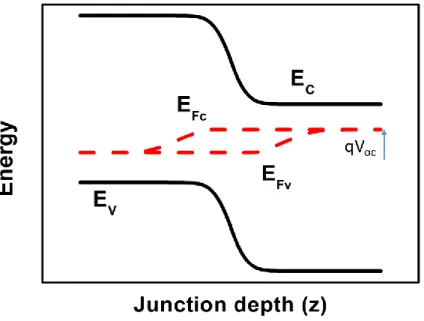
Figure 1.3.1-1: Band diagram of a pn junction under illumination at Voc. Ec, Ev, EFc and EFv
are the conduction band, the valence band, the quasi-Fermi levels for holes and electrons respectively.
1.2 Current-voltage characteristic and Shockley-Queisser limit Solar cells have emerged thanks to the p-n junction. This technology has for long been the only one exhibiting photovoltaics results. Even if this technology is now well-handled, its efficiency limit is quite low. In 1961, Shockley and Queisser proposed a model to determine this technology efficiency limit [17]. This model takes into account the absorption and the radiative transitions for the electron-holes pairs. With this consideration, the current through the diode is equal to the difference between the absorption and the radiative recombination.
1.2. Current-voltage characteristic and Shockley-Queisser limit where J is the electric current density in mA.cm-2, 𝑁̇
𝑒𝑚(𝑉) and 𝑁̇𝑎𝑏𝑠 the emitted
and absorbed photon current density respectively.
For a semiconductor at temperature Tc under an applied voltage V, the emitted
photon flux is defined as:
where n, p and ni holds for the electrons, holes and intrinsic carrier densities
respectively. The photon flux emitted at equilibrium, 𝑁̇0, is given by the Planck’s law, for a black body at temperature Tc:
Concerning the absorbed photon flux, two sources irradiates the sample: the Sun and the thermal radiance of the ambient environment. According to the detailed balance, the ambient photon flux is equal to 𝑁̇0. As for the Sun, if we consider the sun emits a black body spectrum at the temperature Ts, the photon flux incident on
the cell per unit area, unit solid angle and unit photon energy is expressed as:
where E is the photon energy, k the Boltzmann’s constant, Ts the Sun temperature,
θ the incident angle and the azimuthal angle. Once integrated over angles and energy, and assuming an absorptivity of 1 over the band gap energy and zero below, the absorbed photon current density is given by Planck’s Law:
𝑁̇𝑒𝑚(𝑉) = 𝑛𝑝 𝑛𝑖2𝑁̇0 = 𝑒𝑥𝑝 ( 𝑞𝑉 𝑘𝑇𝑐) 𝑁̇0 (1.2-2.) 𝑁̇0 = 1 4𝜋2ℏ3𝑐2∫ 𝐸²𝑑𝐸 𝑒𝑥𝑝 (𝑘𝑇𝐸 𝑐) − 1 ∞ 𝐸𝐺 (1.2-3.) 𝑑𝑁𝑝ℎ = 𝐸² 4𝜋3ℏ3𝑐2( 1 𝑒𝑥𝑝 (𝑘𝑇𝐸 𝑠) − 1 ) 𝑐𝑜𝑠𝜃𝑠𝑖𝑛𝜃𝑑𝜃𝑑𝜑𝑑𝐸 (1.2-4.)
where f is a geometrical factor that accounts for the solid angle subtending the Sun, given by 𝑓 = 𝑠𝑖𝑛²(𝜃𝑠) for an incident light inside a cone of semi-angle s.
Combining Eq (1.1-4), Eq. (1.1-5.) and Eq. (1.1-7.). we obtain:
This expression is the current-voltage characteristic for an ideal diode with 𝐽𝑠𝑐 = 𝑞𝑁̇𝑎𝑏𝑠,𝑠𝑢𝑛and 𝐽0 = 𝑞𝑁̇0
Finally, the power conversion efficiency is expressed as
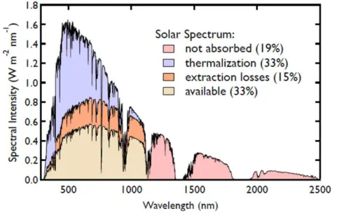
Radiative recombination is affecting both short-circuit current density and open-circuit voltage of the device. Neglecting it and assuming that all absorbed lead to a collected carriers pair, maximal efficiency reaches 44% for a blackbody spectrum at 6000K. Radiative recombinations are nonetheless unavoidable and even needed since the emissivity equals the absorptivity according to the detailed balance principle. For a cell at 300K, the efficiency limit given by the Shockley-Queisser model under AM1.5 is 31% for a band gap EG=1.4eV, while under maximum
concentration this limit reaches 41% for a 1.1eV band gap. It is important to note that 𝑁̇0 and 𝑁̇𝑎𝑏𝑠,𝑠𝑢𝑛 are two quantities depending on the band gap energy, so does the power conversion efficiency. Indeed, it appears that two important processes limit the conversion efficiency: (i) the non-absorption where no photon can be absorbed below the band gap and (ii) the thermalisation where photons with energy higher than the band gap will create electron-hole pairs that eventually will lose
𝑁̇𝑎𝑏𝑠,𝑠𝑢𝑛 = 4𝜋2ℏ3𝑐2∫ ( 𝑒𝑥𝑝 (𝑘𝑇𝐸 𝑠) − 1 ) 𝐸𝐺 𝐸²𝑑𝐸 (1.2-5.) 𝐽(𝑉) = 𝑁̇𝑎𝑏𝑠,𝑠𝑢𝑛− 𝑁̇0(𝑒𝑥𝑝 ( 𝑞𝑉 𝑘𝑡𝑐) − 1) (1.2-6.) 𝜂 =𝑉𝐽(𝑉) 𝑁̇𝑠𝑢𝑛 (1.2-7.)
1.2. Current-voltage characteristic and Shockley-Queisser limit their kinetic energy by heating the lattice. The ratio of the different mechanisms as a function of the bandgap is illustrated in Figure 1.3.1-1. And one can see that the maximum conversion efficiency is obtained for Eg around 1.4 eV.
There exists however different ways to convert sunlight into electrical work that may be more efficient. Several concepts have arisen in order to overcome this low efficiency, all gathered under the third generation solar cell’s label. They aim at limiting the two main losses appearing in single junction cell.
In the case where non-radiative recombinations occur, this model still holds, completed with the radiative efficiency of the cell, defined as [31]:
From this equation, we can expressed the open circuit voltage
The above expression shows that the Voc is linked to the material quality. This will
be important in the third chapter of this thesis, where we will deal with a dilute nitride alloy that suffers from low material quality.
In the Shockley-Queisser (SQ) model, the radiative efficiency,𝑢, equals 1 and the so-called Shockley-Queisser limit represents the maximal efficiency achievable for a simple p-n junction solar cell.
𝑢(𝐸) =𝑁̇𝑒𝑚− 𝑁̇0 𝑁̇𝑎𝑏𝑠 = 𝐽0(𝑒𝑥𝑝 (𝑞𝑉𝑘𝑇𝑜𝑐 𝑐) − 1) 𝐽𝑠𝑐 (1.2-8.) 𝑉𝑜𝑐 = 𝑘𝑇𝑐 𝑞 𝑙𝑛 [ 𝑢(𝐸)𝐽𝑠𝑐 𝐽0 + 1] (1.2-9.)
Figure 1.3.1-1: Detail of the losses happening in a solar cell as a function of the band gap energy. It appears that the maximal efficiency is reached for EG= 1.4eV. From [32].
1.3 Third generation systems
Nowadays several possibilities are explored in order to overcome the Schockley-Queisser limit. Among them we can distinguish different types of solutions: spectral modelling of light (up and down-conversion), high carrier density systems (hotcarrier and multipleexciton generation) and multitransition systems (multi -junction and Intermediate band devices).
A simple way to understand the p-n junction’s limit is to consider the inherent trade-off between open-circuit voltage and short-circuit. This situation is well illustrated by Figure 1.3.1-1, which depicts the spectral efficiency of photovoltaic conversion and points out that the main losses are due to non-absorption, that affects the short-circuit current, and thermalisation processes, that is a loss of potential energy directly linked to the open-circuit voltage. As these two processes are opposite to each other as respect to the band gap energy, a trade-off has to be made. The optimised trade-off is met for a band gap energy of 1.4eV for the AM1.5 spectrum. Now if we consider that several transitions occur in the same device, each transition energy will convert only a part of the solar spectrum, making
non-1.3. Third generation systems absorption and thermalisation losses decrease. Two concepts using multi-transition process exists nowadays: the multijunction solar cells and the intermediate band solar cells. These concepts will be detailed below.
Figure 1.3.1-1: Spectral conversion efficiency and losses in the photovoltaic process for a Silicon based p-n junction.
1.3.1 Multijunction solar cells
This is the oldest and most mature third generation solar cell concept. It has been originally developed for extra-terrestrial applications, especially for satellite power supply. Up to now, multijunction solar cells are the only third generation concept that have passed the Schockley-Queisser limit, and exhibited efficiencies up to 46% for four-junction solar cells and 44.4% for three-junctions [9]. As for the modules, the record efficiency is 36.7% [9].
(a) (b)
Figure 1.3.1-1: Structure of the record four-junction solar cell (a) and its corresponding J-V curve, measured under 289 suns (b). From [33].
The basic principle of multijunction solar cells is depicted Figure 1.3.1-2. We consider here the case of two subcells for simplicity. The top cell absorbs the high energy part of the solar spectrum, whereas the bottom cell absorbs the rest. The two cells are working in series, meaning that the total current of the device equals the lower current of the two subcells whereas its voltage equals the sum of the two subcells’ voltage. To avoid non collected absorption and reach an optimised efficiency the two subcells should hence generate the same current. This condition is called current-matching and is a fundamental principle of tandem solar cell. To fulfil this condition, we can vary two parameters: the band gap energies and thicknesses of the two subcells. In our case, since we assume full absorption in the two subcells, we can only consider the band gap energies. The serial connection is ensured by the tunnel junction. Its role is to allow recombination between electrons and holes at the interface between the two subcells (cf. Figure 1.3.1-2.). Without the tunnel junction, the two diodes would just work as one with the lower band gap energy. Of course, the tunnel junction should have a large band gap energy, which insures non parasitic absorption and surface passivation, and should be very thin in order to allow for the carriers to tunnel through (typically few ten nanometres).
1.3. Third generation systems
Figure 1.3.1-2: Energy band diagram for a tandem cell. The role of the tunnel junction in the serial connection between the two subcells is outlined here. From [34].
Efficiency limit calculation
Here we apply the same method as presented Sec.1.1 adding the specific behaviour a tandem solar cell [10], [35]–[37]. We assume that both subcells are thick enough to fulfil the total absorption condition above their band gap energies. The bottom cell absorbs only between 𝐸𝐺1 and 𝐸𝐺2. The current is not anymore related to the total absorption in the device but equals the lower subcells’ absorption. An infinite carrier mobility is supposed, i.e. the µ is uniform within the materials’ volume. In that case, as seen previously, the subcells’ voltage qVsubcell=µsubcell and
qV=µ1+µ2. Finally, we neglect photon recycling.
Therefore, Eq.(1.2-1.) becomes:
with
Whereas the emitted photon flux is expressed as:
Maximum efficiency for a two junction tandem solar cell is found to be 45.3% efficiency for E1=0.94eV and E2=1.61eV for AM1.5 spectrum [10]. The
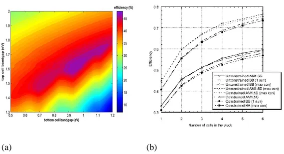
dependence of a two-junction solar cell efficiency on the band gap energies depicted on Figure 1.3.1-3(a). If more junctions are added, the efficiency will increase up to 87% for an infinite number of junctions [35] (cf. Figure 1.3.1-3 (b)). This technology is therefore very interesting, but suffers from expensive fabrication methods, especially because of the need of two substrates for the record four-junction solar cell for instance. From this point of view, the intermediate band solar cell is more promising.
𝑁̇𝑎𝑏𝑠𝑡𝑜𝑝= 4𝜋2ℏ3𝑐2∫ 𝑒𝑥𝑝 (𝑘𝑇𝐸 𝑠) − 1 𝐸𝐺2 (1.3-2.) 𝑁̇𝑎𝑏𝑠𝑏𝑜𝑡𝑡𝑜𝑚= 𝑓 4𝜋2ℏ3𝑐2∫ 𝐸²𝑑𝐸 𝑒𝑥𝑝 (𝑘𝑇𝐸 𝑠) − 1 𝐸𝐺2 𝐸𝐺1 (1.3-3.) 𝑁̇𝑒𝑚(𝑉 = 𝜇1+ 𝜇2) = 1 4𝜋2ℏ3𝑐2 [∫ 𝐸²𝑑𝐸 𝑒𝑥𝑝 (𝐸 − ∆𝜇𝑘𝑇 1 𝐶 ) − 1 ∞ 𝐸𝐺1 + ∫ 𝐸²𝑑𝐸 𝑒𝑥𝑝 (𝐸 − ∆𝜇𝑘𝑇 2 𝐶 ) − 1 ∞ 𝐸𝐺2 ] (1.3-4.)
1.3. Third generation systems
(a) (b)
Figure 1.3.1-3: (a) Mapping of the conversion efficiency for a two-junction solar cell as a function of the band gap energies of the two subcells. From [38]. (b) Evolution of the thermodynamic efficiency of multijunction solar cells as a function of the number of junctions. From [10].
1.3.2 Intermediate band solar cells
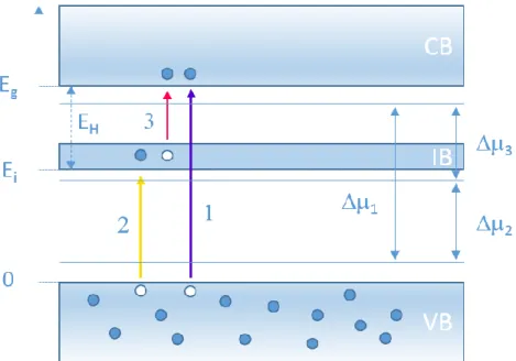
In an intermediate band solar cell (IBSC), all the transitions are occurring in the same material. The idea is to insert one or a few band levels in the middle of the bandgap energy EG of the host material. Three strategies have been investigated:
quantum-confined heterostructures (quantum dots and quantum wells), highly mismatched alloys, and addition of impurities. The IBSC principle is depicted in Figure 1.3.2-1. In addition to the classical transition from the valence band to the conduction band of energy EG, two transitions occur through the intermediate band,
of energy EI and EH, giving rise to only one electron-hole pair. Electrically this
device is equivalent to a two junction tandem solar cell in parallel to the host material diode (cf. Figure 1.3.2-2(a)). From this equivalent electrical scheme we can derived the following set of equation:
Figure 1.3.2-2 displays the J-V characteristics for an ideal IBSC. Compared to the host material, the IBSC exhibits a higher Jsc, as expected from the above equations,
but a slightly lower Voc. This is because of the additional radiative recombination.
Figure 1.3.2-1: Scheme of the Intermediate band solar cell working. The three transitions involved in the IBSC concept are depicted, with their associated µ.
𝐽 = 𝐽1+ 𝐽2,3 (1.3-6.)
1.3. Third generation systems
Figure 1.3.2-2: (a) Equivalent electrical circuit of an IBSC. The two transitions implying the IB represented by two diodes in serial connection, in parallel with the diode of the host material transition. (b) J-V curve of an ideal IBSC compared with the high (low) band gap cell. From [39].
1.3.2.1 Thermodynamic limit of IBSC
We want now to determine the efficiency limit of the IBSC. The assumptions made in Sec.1.2 are still applicable here. In addition, specific assumptions are made: no absorption overlap exists, meaning an optimised absorption of the solar spectrum: if assume EH < EI and E the photon energy, if E <EH no absorption occurs, for EH
< E <EI the photon is absorbed from the IB to the CB, for EI < E < EG photons are
absorbed by the IB and if E > EG absorption is made by the host material.
Following the equivalent electrical scheme, we write the devices’ total current as:
with
The limit efficiency of such a device is calculated at 49% for AM1.5 [40], and reaches 63.2% for a black body radiation at 6000K under maximal concentration. With the same approach, the efficiency of a two intermediate bands solar cell has been evaluated at 71.7% by Brown et al [41]. Lee and Honsberg have even calculated the theoretical limit of tandem solar cell composed of two IBSCs, reaching 73.4% [42]. 𝑁̇𝑎𝑏𝑠𝑉𝐶 = 4𝜋2ℏ3𝑐2∫ 𝑒𝑥𝑝 (𝑘𝑇𝐸 𝑠) − 1 𝐸𝐺 𝑁̇𝑎𝑏𝑠𝑉𝐼 = 𝑓 4𝜋2ℏ3𝑐2∫ 𝐸²𝑑𝐸 𝑒𝑥𝑝 (𝑘𝑇𝐸 𝑠) − 1 𝐸𝐺 𝐸𝐼 (1.3-10.) 𝑁̇𝑎𝑏𝑠𝐼𝐶 = 𝑓 4𝜋2ℏ3𝑐2∫ 𝐸²𝑑𝐸 𝑒𝑥𝑝 (𝑘𝑇𝐸 𝑠) − 1 𝐸𝐼 𝐸𝐻 (1.3-11.) and 𝑁̇𝑒𝑚(𝑉 = 𝜇𝐶𝑉) = 1 4𝜋2ℏ3𝑐2 [∫ 𝐸²𝑑𝐸 𝑒𝑥𝑝 (𝐸 − ∆𝜇𝑘𝑇 𝐼𝐶 𝐶 ) − 1 ∞ 𝐸𝐻 + ∫ 𝐸²𝑑𝐸 𝑒𝑥𝑝 (𝐸 − ∆𝜇𝑘𝑇 𝑉𝐼 𝐶 ) − 1 ∞ 𝐸𝐼 + ∫ 𝐸²𝑑𝐸 𝑒𝑥𝑝 (𝐸 − ∆𝜇𝑘𝑇 𝐶𝑉 𝐶 ) − 1 ∞ 𝐸𝐺 ] (1.3-12.)
1.3. Third generation systems 1.3.2.2 Practical limit of IBSCs’ efficiency
Absorption coefficient overlapping
We saw that, for a maximum efficiency, each transition should absorb only the spectral part that correspond to its energy. In the case of tandem solar cells, this is quite easy to do in practice: we should only have sufficient absorber thickness for each junction. For the IBSC on the other hand, as all the transitions occur in the same material, is much more challenging. Lin and Philips have proposed a specific design to tackle the latter quantity this issue [43]. Concerning the transition between the valence band (VB) and the conduction band (CB), this problem can be treated by adding a layer of host material only on the top of the device. Therefore all the photons of energy higher than EG will be absorbed before the IB material,
avoiding those photons to be involved in the two other transitions. As for the two remaining transitions, the idea would be to create an energy gradient in the IB, while allowing conduction in it. This idea is depicted Figure 1.3.2-3.
Figure 1.3.2-3: Specific design limiting the absorption coefficient overlap. This figure has been adapted from [44].
Dependence on the intermediate band carrier population
As said previously, the two transitions involving the intermediate band are working as tandem cell. The efficiency of this cell will therefore depend on the current matching between these two diodes. In this case nonetheless, this current matching condition will not only be up to the combination of the two band gap energies or thicknesses. As the intermediate band has by definition a finite density of states, both absorption from and towards this IB will depend on the carrier population in it.
Figure 1.3.2-4: Schematic of an IBSC represented with the different generation an recombination rates.
We can see that the IBSC design is a fragile balance between the different relaxation times, absorption coefficient and band gap energies association. All those quantities are defined for a given temperature and at a given carrier injection level. Optimisation of an IBSC is hence very complex and must be carefully thought. Having significant density of states in the intermediate band is also crucial here, because in addition to allow a significant current density, it decreases the dependence on the carrier population in the IB.
𝑑𝑛𝐼
𝑑𝑡 = 𝐺𝑉𝐼 + 𝑅𝐶𝐼 − 𝐺𝐼𝐶 − 𝑅𝐼𝑉+ 𝑅𝑡ℎ𝐶𝐼− 𝑅𝑛𝑟𝐼𝑉
1.3. Third generation systems In conclusion, we have seen that the luminescence is directly related to the open-circuit voltage of a cell, and therefore to the material quality. Combined with the knowledge of the incident photon flux and the absorptivity of the sample, linked to the short circuit current, we can perform an all optical J-V measurement. This is particularly interesting for third generation solar cells that barely exist in complete form up to day. Furthermore, multi-transition solar cells are exhibiting high conversion efficiencies with 63% for IBSC and 46% for a two-junction solar cell. Those conversion efficiencies are however strongly dependent on the behaviour of each transitions. We understand that in order to characterise multi -transition devices, we need to study all the radiations separately. In this perspective, luminescence based characterisations are a powerful and versatile tool.
Chapter 2
2
Experimental setups and methods
In this thesis, we will focus on the characterization of several type of solar cells. The variety of these solar cells, of their physics and their specific problematics will lead us to use a large spectrum of characterisation methods. In this chapter, we will present those methods and the associated experimental setups.
First we will introduce the classical tools for opto-electrical characterisation of solar cells: current-voltage characteristics, quantum efficiency and absorption measurement.
The largest part of this chapter will then be dedicated to the photoluminescence (PL) and its intensity, spatial and spectral properties. A classical homemade confocal microscope is first described. The versatility of this setup allows us to use it for several analysis that we will detail: PL measurement, time-resolved photoluminescence (TRPL), photoluminescence excitation (PL-E) and local EQE measurements.
We will then introduce an original and powerful experimental tool, the hyperspectral imager that records spectrally resolved luminescence images with an absolute measurement of the emitted photon flux. The absolute calibration of this setup will be detailed.
2.1 Classical solar cell characterisations
Standard characterisation setups dedicated to solar cells are used to investigate the samples. We can distinguish two main characterisations: EQE and J-V characteristic measurements.
2.1.1 Quantum efficiency measurements
External and internal quantum efficiencies (EQE and IQE) measurements are key characterisations of solar cells. Those quantities are defined as follow:
I() is the recorded current, N() is the total number of incident photons and A() the absorption in the sample. In other words, EQE () gives the ratio of collected carriers on incident photons per wavelength. With the IQE measurement we free ourselves of optical losses, making this characterisation very interesting in view of investigating the recombination mechanisms and the carrier transport properties. These physical quantities are crucial for the development of a new material and will be used in the Chapter 3, dedicated to the GaAsPN solar cell. EQE measurements will also be used as an approximation for the absorption, under specific conditions.
EQE are measured by an Oriel IQE200 from Newport. This setup allows us to work in the 300-2500nm range. A Xenon Lamp is used for the excitation, and the selection of the wavelength is made by a monochromator. The calibration of the incident power is done by two detectors, one made in silicon for the 400-1100nm range, and one made in Germanium for the 1100-2500 nm range. In addition, we can use an integrating sphere to record scattered and specular reflection. With this
𝐸𝑄𝐸(𝜆) = 𝐼(𝜆) 𝑁(𝜆) (2.1-1.) 𝐼𝑄𝐸(𝜆) = 𝐼(𝜆) 𝑁(𝜆) ∗ 𝐴(𝜆) (2.1-2.)
2.1. Classical solar cell characterisations
reflectometry measurement, assuming that the transmission is null, we can calculate the internal quantum efficiency:
Local EQE
External quantum efficiency gives macroscopic measurements of a solar cell’s performances. But, if the sample is not homogeneous, a local EQE can be more instructive. This can be the case in complex alloy, for which clusters and composition fluctuation can appear [45], or in a quantum confined heterostructures where a spatial inhomogeneity of the quantum structure dimensions can be observed. This experiment can be performed by a white light source (lamp or supercontinuum laser) coupled with a microscope.
2.1.2 J-V characteristics
Electrical J-V measurement is the ultimate performance test for solar cells. The cells efficiencies are determined by a Oriel Sol3A solar simulator manufactured by Newport. It is an AAA solar simulator. This rate designates the spatial homogeneity, spectral and intensity specifications. We used a Keithley 2635B sourcemetre to acquire the electrical signal and a chiller to maintain the sample temperature at 25°C.
The J-V characteristics determined in optical considerations only (cf. Sec. 1.2) are an ideal case. From the absorber to the terminal, the carrier encounter several loss sources that have to be considered. We will now make the parallel with the first chapter where we used a pure optical model.
𝐼𝑄𝐸(𝜆) = 𝐸𝑄𝐸(𝜆)
1 − (𝑅𝑠𝑐𝑎𝑡𝑡𝑒𝑟𝑒𝑑(𝜆) + 𝑅𝑠𝑝𝑒𝑐𝑢𝑙𝑎𝑟(𝜆))
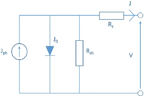
As we deal here with classical electrical model, we include resistances in the electrical equivalent circuit for the solar cell, following the schematic in Figure 2.1.2-1.
Figure 2.1.2-1: Equivalent electrical circuit of a solar cell for a one diode model. Jph and J0
are the photocurrent and the saturation current, while Rs and Rsh are the series and shunt
resistances respectively.
In dark conditions, the current-voltage characteristic is expressed by the following relation supposing a one-diode model [19]:
Where J0 is the saturation current, Rs the series resistance and Rsh the shunt
resistance.
If we assume only radiative recombinations, 𝐽𝑑𝑎𝑟𝑘(𝑉) = 𝐽0exp [(𝑞(𝑉 − 𝑅𝑠𝐽) 𝑛𝑘𝑇 ) − 1] − 𝑉 − 𝑅𝑠𝐽 𝑅𝑠ℎ (2.1-4.) 𝐽0 = 𝐽0𝑟𝑎𝑑 = ∫ 𝐸𝑄𝐸(𝐸)𝛷𝐵𝐵(𝐸, 𝑇 = 300𝐾)𝑑𝐸 ∞ 𝐸𝑔 (2.1-5.)
2.1. Classical solar cell characterisations
Under illumination, a minority carriers current Jphotocurrent arises in the opposite
direction to Jdark such as the complete current expression is:
The photocurrent is a general term that includes the voltage dependence of the photogenerated current 𝑞𝑁̇𝑎𝑏𝑠,𝑠𝑢𝑛. The voltage dependence, called the carrier collection efficiency, will be used in chapter 3 and is expressed by:
In most cases, there is no problem of collection at V=0V and 𝑞𝑁̇𝑎𝑏𝑠,𝑠𝑢𝑛 = 𝐽𝑠𝑐, so this relation is often expressed in function of Jsc, instead of the photogenerated
current. Jsc is the short-circuit current:
This value is important because it defines the current of the diode at the beginning of the power production area. Its theoretical limit, when no collection losses are exhibited by the solar cell at 0V, is: 𝐽𝑠𝑐,𝑚𝑎𝑥 = 𝑞𝑁̇𝑎𝑏𝑠,𝑠𝑢𝑛. The end of this region is given by the open circuit voltage Voc.The open-circuit voltage is found by solving
Eq. (2.1-6.) with J(Voc)=0:
The theoretical maximum of the open circuit voltage is reached when only radiative recombinations and no collection losses are present in the cell:
𝐽(𝑉) = 𝐽𝑑𝑎𝑟𝑘(𝑉) − 𝐽𝑝ℎ𝑜𝑡𝑜𝑐𝑢𝑟𝑟𝑒𝑛𝑡(𝑉) (2.1-6.) 𝜌(𝑉) =𝐽𝑝ℎ𝑜𝑡𝑜𝑐𝑢𝑟𝑟𝑒𝑛𝑡(𝑉) 𝑞𝑁̇𝑎𝑏𝑠,𝑠𝑢𝑛 (2.1-7.) 𝐽𝑠𝑐 = ∫ 𝐸𝑄𝐸(𝐸)𝛷𝑠𝑢𝑛(𝐸)𝑑𝐸 ∞ 𝐸𝑔 (2.1-8.) 𝑉𝑜𝑐 = 𝑛𝑘𝑇 [𝑙𝑛 (𝐽𝑝ℎ𝑜𝑡𝑜𝑐𝑢𝑟𝑟𝑒𝑛𝑡(𝑉𝑜𝑐) 𝐽0 ) + 1] (2.1-9.)
This value will be compared to the obtained Voc in Chapter 3. Rau et al have also
demonstrated that the difference between those two values are linked to the external quantum efficiency of LEDs [46].
2.2 Spectrophotometry
Optical characterisations, such as reflexion, transmission or absorption of solar cell material are primordial. Absorption loss is the first phenomenon to consider in a solar cell. There are multiple characterisation methods to get to the absorption: direct, such as spectrophotometer, ellipsometry measurements or indirect, for instance with PL intensity using the generalised Planck’s law. A spectrophotometer uses a calibrated light source that pass through a grating which transmits a thin spectral interval. The light is then guided to the sample that is placed at the front (back) of an integrating sphere where the transmitted (reflected) light will be measured. By its lambertian inner surface, the integrating allow the light to be indefinitely reflected until it reaches the detector. The light intensity is compared with a reference beam, and the transmission (respect. the reflexion) is calculated. From these measurements we can extract the absorption coefficient of the sample. This value is a key parameter. Indeed, it governs the absorber thickness needed to absorb the excitation light. Therefore, it is a necessary value in numerical simulation and solar cell structure design. Figure 2.1.2-1 describes the spectrophotometer design. Its spectral resolution goes down to 0.05nm, depending on the experimental parameters.
I0 is the incident light intensity, IR the reflected light intensity and IT the transmitted
one. In the simplest configuration, with only one material, we can deduct from the Beer-Lambert‘s law the absorption coefficient of the sample:
𝑉𝑜𝑐𝑟𝑎𝑑 = 𝑘𝑇 [𝑙𝑛 (𝑞𝑁̇𝑎𝑏𝑠,𝑠𝑢𝑛
𝐽0𝑟𝑎𝑑 ) + 1]
(2.1-10.)
2.2. Spectrophotometry
For complex samples with different layers, one has to take into account the possible reflexion at each interfaces, and also the potential interferential patterns. Hypothesises taken for our samples will be detailed in the corresponding sections.
(a)
(b)
Figure 2.1.2-1: (a) Sketch of the lambda 900 spectrophotometre. (b) Sample considered and physical values of interest.
2.3 Photoluminescence
In this section, we will describe the different techniques based on PL used in this thesis. Several systems and setups exist, whether we are interested in the intensity, spectral or spatial properties of the luminescence. Based on the luminescence of the solar cell introduced in the previous chapter, we will explain how, from this PL signal, we can extract the desired physical quantities for each experimental setup. 2.3.1 Confocal microscope
The system used in this work is a homemade classical confocal microscope featured Figure 2.3.1-1 that allows the different experimental characterization technics described below. Here the pinholes, responsible for the “confocal” mode, are replaced by optical fiber of diameter between 6 and 60µm depending on the application. In this range of diameter, the confocal mode is guaranteed. Its theory is widely exposed in literature [47]–[50].
Figure 2.3.1-1 : Sketch of the confocal microscope. The role of the pinholes on the axial resolution is outlined here. From [51]
2.3. Photoluminescence
The main specifications for this setup are the excellent lateral and axial resolutions, given by [47]:
Where NA is the numerical aperture of the system, exc the excitation wavelength,
and n the refraction index of the analysed material. This homemade microscope is particularly versatile and will support all the setups described in the following. 2.3.1.1 Photoluminescence spectra measurements
As demonstrated previously, luminescence is a powerful tool to estimate the performances of the solar cells such as the absorbance, the open-circuit voltage or the photocurrent. Crystalline orientation can even be probed when combined with polarisation analysis [52]–[54].
For the simple PL spectra measurement, a laser excitation is coupled into the injection optical fibre. The laser beam is then collimated using a lens chosen to adapt the spot diameter with the objective pupil. The laser is then directed towards a beamsplitter where it is reflected to the sample. The generated luminescence is collected by the objective, get through the beamsplitter and is coupled into the collection optical fibre. A spectrometer from Princeton Instruments records the luminescence spectra with a spectral resolution down to 0,14nm with a 1200g/mm grating at 450nm [55].
All the PL spectra are spectrally corrected. The spectral calibration aims to determine the spectral response of the system. We use a calibrated lamp coupled in an integrating sphere, which is a sphere with inner surface close to a lambertian reflector. The light is reflected numerous times before escaping the sphere. The
𝛥𝑥 =0.42𝜆𝑒𝑥𝑐 𝑁𝐴 (2.3-1.) 𝛥𝑧 =1.4𝑛𝜆𝑒𝑥𝑐 𝑁𝐴² (2.3-2.)
intensity, radiance, spectrum and angular distribution. All the spectral modification observed is induced by the optical system. This spectrum is designated as
Reference spectrum (x, y, ), and the Recorded spectrum (x, y, is the acquisition
made by the spectrometer, with:
Each acquisition will be corrected by the system response:
2.3.1.2 Photoluminescence excitation
Photoluminescence excitation (PL-E) consists in recording the PL signal while varying the excitation wavelength. We will use this characterisation tool to apprehend the absorption in the layer of interest. Indeed a look to the generalised Planck’s law shows that the only physical quantity that should change with the wavelength is the absorption. Also, as the luminescence is layer selective, we can access the absorbance of a particular layer in a stack. Finally, excitonic features can be accessed with PL-E measurements [56]. However, the variation of luminescence intensity obtained has to be corrected by the incident power, and quantitatively calibrated. The calibration can be done by normalizing with a known value of the absorption (typically at short wavelength the absorption is set to 1). In this thesis we are particularly interested in the resonant PL-E measurement. The complexity in this case consists in recording the luminescence without being disturbed by the laser reflexion. Pr. Heitz and his team have recorded the PL signal coming from excited states of quantum confined heterostructures and corrected this signal by the thermionic transition [57]. One can also use phonon replica for reconstruct the PL-E spectrum [58]. Another possibility to extinct the laser
𝑅(𝜆) = 𝑅𝑒𝑐𝑜𝑟𝑑𝑒𝑑𝑠𝑝𝑒𝑐𝑡𝑟𝑢𝑚(𝜆) 𝑅𝑒𝑓𝑒𝑟𝑒𝑛𝑐𝑒𝑠𝑝𝑒𝑐𝑡𝑟𝑢𝑚(𝜆) (2.3-3.) 𝐶𝑜𝑟𝑟𝑒𝑐𝑡𝑒𝑑𝑠𝑝𝑒𝑐𝑡𝑟𝑢𝑚(𝜆) =𝑅𝑒𝑐𝑜𝑟𝑑𝑒𝑑𝑠𝑝𝑒𝑐𝑡𝑟𝑢𝑚(𝜆) 𝑅(𝜆) (2.3-4.)
2.3. Photoluminescence
reflexion is the use of two linear polarisers, one to control the polarisation of the incident laser and one orthogonally positioned to block the lasers’ reflexion. As we work at room temperature, the luminescence induced by a linearly polarised laser does not keep this polarisation, and the PL signal will only be reduced. We chose this configuration for our experiments.
The experimental setup used to perform PL-E relies on the confocal microscope. The excitation source is a Fianium supercontinuum laser whose wavelength is selected using a Photon Etc Laser Line Tunable Filter. This laser works in the 450-2500nm range. The spectral resolution is 2 nm while the extinction ratio is higher than 105. The laser is coupled into an optical fibre connected to the confocal
microscope. Here, because of the large range excitation wavelength, we use a 50:50 beamsplitter operating in the 350-1100nm range. The sample is then excited using a microscope objective (either reflective or apochromatic, both giving the same results). The two polarisers have an extinction ratio higher than 105.
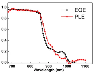
A typical PL-E curve measured on a multiple quantum wells sample is depicted Figure 2.3.1-2. The corresponding EQE is plotted on the same axis. A good correlation is found between the two quantities, even in the quantum wells levels spectral region.
2.3.1.3 Time-resolved photoluminescence
Time-resolved photoluminescence (TRPL) is a useful technique to access the carrier dynamics. It consists in recording the PL as a function of time. There are four main technics for recording TRPL:
- Streak camera
- Time-correlated single photon counting - Pump-probe
- Up-conversion
Streaks cameras are able to record the temporal evolution of the PL spectra. Their time resolutions are good, going down to 3 ps whereas the fastest luminescence decay characteristic times are around hundred ps. The conservation of the spectral information is another great advantage of the streak cameras.
Time-correlated single photon counting on the other hand is based on the detection of single photons of a light signal periodically induced by the supercontinuum laser described in the previous section. Based on the measurement of the detection time,
700 800 900 1000 1100 0,0 0,2 0,4 0,6 0,8 1,0 Wavelength (nm)
EQE
PLE
Figure 2.3.1-2: Comparison between PLE and EQE for a multi-quantum wells sample, introduced and detailed in chapter 4.
2.3. Photoluminescence
the reconstruction of the temporal evolution of this signal is made. The photons counted are not energetically discriminated and the spectral information is thus lost. By adding a monochromator, we can reconstruct the spectral information. The force of this technic is its very good sensitivity.
This is the technology we used for the TRPL measurements during this thesis. The pulsed source is the supercontinuum laser introduced in the previous section. The single photon counting detector used is an ultra-low noise silicon avalanche photodiode -SPAD from Picoquant. The overall temporal resolution of our system is 350ps.
2.3.2 Hyperspectral Imager
The hyperspectral imager (HI) is an original tool that records intensity, spectral and spatial properties of the luminescence in one acquisition. Moreover, this setup can be absolutely calibrated to measure the luminescence flux. This highly valuable property will be particularly used in this thesis.
2.3.2.1 Setup
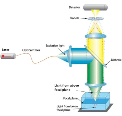
The basic principle of the HI is to record images of PL at various detection wavelength, which all together form a cube. Hyperspectral Imagers are known, especially in the biology research field [59], [60], but only little known in the photovoltaics field [27], [28], [61]–[63]. Those systems can probably not be absolutely calibrated, or at least do not use this property. Our system has been developed by Photon etc, in collaboration with IRDEP during Dr. Delamarre ’s thesis [64] for photovoltaics applications. It relies on volume Bragg gratings. A schematic of the whole setup is displayed Figure 2.3.2-1.
The sample is illuminated by a laser source through a microscopic objective, after a reflection by a beamsplitter. The luminescence is collected by the same objective. The hyperspectral image is formed by volume Bragg gratings and recorded by a
Figure 2.3.2-1: Principle of Hyperspectral imaging: experimental configuration for uniform sample excitation, a hyperspectral imager, and a CCD detection. An hypercube of data (x,y,λ,Intensity) is acquired with a CCD camera as explained in the text. At each spatial location, a luminescence spectrum with calibrated data is obtained. Conversely, maps of luminescence intensities for each wavelength can be extracted.
2.3.2.2 Device calibration
In order to accurately acquire the spectral, spatial, and intensity information of the luminescence, the HI has to be calibrated. This calibration method is decomposed in two steps: a spectral calibration and an absolute one.
This calibration is similar to the one detailed for the confocal microscope. This time, however, R(x, y, ) applies to an image, and the calibration has to take into account the spatial information. So, the HI images the output surface of the integrating sphere. With such a surface, all the variations recorded on the camera will have been introduced by the optical system. This image is designated as
Reference image (x, y, ), and the Recorded image (x, y, is the acquisition made
2.3. Photoluminescence
Each acquisition will be corrected by the system response:
The second step, the absolute calibration, is then done to complete the calibration. This calibration will convert the intensity from counts to photons emitted per second, surface volume and energy interval. The whole procedure is detailed in [65]. Basically, the idea here is to record the output of an optical fibre coupled to a laser. Knowing the optical power at this output, measured with a powermeter, we can consequently determine the ratio of emitted light that is recorded, and then correct the acquired cubes.
𝑅(𝑥, 𝑦, 𝜆) = 𝑅𝑒𝑐𝑜𝑟𝑑𝑒𝑑𝑖𝑚𝑎𝑔𝑒(𝑥, 𝑦, 𝜆) 𝑅𝑒𝑓𝑒𝑟𝑒𝑛𝑐𝑒𝑖𝑚𝑎𝑔𝑒(𝑥, 𝑦, 𝜆) (2.3-5.) 𝐶𝑜𝑟𝑟𝑒𝑐𝑡𝑒𝑑𝑐𝑢𝑏𝑒(𝑥, 𝑦, 𝜆) =𝑅𝑒𝑐𝑜𝑟𝑑𝑒𝑑𝑐𝑢𝑏𝑒(𝑥, 𝑦, 𝜆) 𝑅(𝑥, 𝑦, 𝜆) (2.3-6.)
Chapter 3
3
Dilute nitride for multi-transitions
photovoltaic systems
Dilute nitride semiconductors has generated ongoing interest because of unique structural and opto-electronical properties. Indeed the addition of a small fraction of nitrogen in standard III-V semiconductors, as GaAs, implies a huge effect on the bandgap energy and the lattice parameter. By introducing several competing atoms among which one with high electronegativity (for instance Nitrogen or Oxygen) for a same crystalline site, one can tune the lattice constant, whereas the band gap energy tuning is due to the localisation of the electronic states. Those effects make dilute nitride very convenient in a large range of opto-electronical devices, such as lasers [66]–[69], communication devices [70], [71] and in multi-junction solar cells [72]–[74], where the control of band gap energy and the lattice parameter is crucial [75]–[77]. Therefore we find dilute nitride in several multi-junction solar cells systems, which are grown on Ge or GaAs substrate. These very expensive substrates make multi-junction solar cells uncompetitive compared to single junction Silicon solar cells. We want to take advantages of the dilute nitride to develop a tandem cell grown on a silicon substrate, hence benefiting of the excellent III-V semiconductor opto-electronical properties and of the silicon solar cells mature technology and competitiveness.
Then we will present numerical simulations of typical GaAsPN-based solar cells and their opto-electrical characterizations. This part will show classical measurements such as J-V characteristics and EQE as well as other fundamental characterizations such as spectrally and time resolved photoluminescence.
Afterwards, we will discuss the results on specific points like the annealing effects, the collection issues, the material heterogeneity and the correlation between optical characterisations and cells parameters.
Finally, a perspective towards the use of such devices as Intermediate Band Solar Cells will be presented.
3.1 Dilute nitride alloys
This first section introduces general dilute nitride properties and the description of the investigated samples.
3.1.1 Dilute nitride III-V alloy for multi-junction solar cells
Nowadays, several MJSCs structures are taking advantage of the specific physics of dilute nitride. As we see Figure 3.1.1-1(a), we can find a dilute nitride alloy lattice-matched to any of the main substrate (GaAs, Ge, InP and Si). The specific behaviour and the versatility of dilute nitride semiconductors is demonstrated on this graph. Standard alloys are following the Vegard’s law regarding the evolution of their lattice constant and bandgap energy. This law simply assumes the linearity of those physical values with the concentration of their elements. For example, let’s focus on the InxGa1-xAs alloy. According to Vegard’s law, its bandgap energy and
lattice parameter, a, should follow:
3.1. Dilute nitride alloys
This parametric evolution is displayed on the graph, but instead of being a straight line it is slightly curved. To be more accurate an additional term has to be considered for the bandgap energy equation and Eq.(3.1-1.) becomes:
b is called the bowing parameter. For standard alloys, this parameter is close to 0. But for highly mismatch alloys (HMA), among which belong dilute nitride alloys, it can reach giant values and modify completely the bandgap energy variation with the composition, as for GaPN. Thanks to this behaviour, GaAsPN can be lattice-matched on Si for a large range of bandgap energy (cf. Figure 3.1.1-1(a)).
(a) (b)
Figure 3.1.1-1: (a) Bandgap energy of elemental and III-V compound semiconductors over lattice constants. From [78]. (b) Efficiency of tandem solar cell as a function of the two subcells band gap. From [38].
𝑎𝐼𝑛𝑥𝐺𝑎1−𝑥𝐴𝑠 = 𝑥𝑎𝐼𝑛𝐴𝑠+ (1 − 𝑥)𝑎𝐺𝑎𝐴𝑠 (3.1-2.)
![Figure 1.3.1-2: Evolution of the total installed PV capacity in the world (MWp) [8].](https://thumb-eu.123doks.com/thumbv2/123doknet/7765142.255830/13.892.188.740.169.470/figure-evolution-total-installed-pv-capacity-world-mwp.webp)
![Figure 1.3.2-3: Specific design limiting the absorption coefficient overlap. This figure has been adapted from [44]](https://thumb-eu.123doks.com/thumbv2/123doknet/7765142.255830/32.892.219.617.653.972/figure-specific-design-limiting-absorption-coefficient-overlap-adapted.webp)