HAL Id: tel-02997877
https://tel.archives-ouvertes.fr/tel-02997877
Submitted on 10 Nov 2020HAL is a multi-disciplinary open access archive for the deposit and dissemination of sci-entific research documents, whether they are pub-lished or not. The documents may come from teaching and research institutions in France or
L’archive ouverte pluridisciplinaire HAL, est destinée au dépôt et à la diffusion de documents scientifiques de niveau recherche, publiés ou non, émanant des établissements d’enseignement et de recherche français ou étrangers, des laboratoires
devices applications compatible with low temperature
(
≤300 ˚C) flexible substrates
Kai Yang
To cite this version:
Kai Yang. Fabrication and characterization of silicon nanowires for devices applications compatible with low temperature (≤300 ˚C) flexible substrates. Electronics. Université Rennes 1, 2019. English. �NNT : 2019REN1S123�. �tel-02997877�
T
HESE DE DOCTORAT DE
L'UNIVERSITE
DE
RENNES
1
COMUE UNIVERSITE BRETAGNE LOIRE
ECOLE DOCTORALE N°601
Mathématiques et Sciences et Technologies de l'Information et de la Communication Spécialité : Electronique
« Fabrication and characterization of silicon nanowires for
devices applications compatible with low temperature (≤300 ˚C)
flexible substrates »
Thèse présentée et soutenue à Rennes le 13 décembre 2019 Unité de recherche : IETR, UMR 6164
Thèse N° :
Par
Kai YANG
Rapporteurs avant soutenance :
Yvan Bonnassieux Professeur, Ecole Polytechnique Henri Happy Professeur, Université Lille
Composition du Jury :
Président : Antoine Goullet Professeur, Polytech Nantes Examinateurs : Yvan Bonnassieux Professeur, Ecole Polytechnique
Henri Happy Professeur, Université de Lille Antoine Goullet Professeur, Polytech Nantes
Nathalie Coulon Ingénieur de recherche CNRS, IETR Dir. de thèse : Laurent Pichon Professeur, Université de Rennes 1
Résumé du mémoire de thèse intitulé
Fabrication and characterization of silicon nanowires for devices
applications compatible with low temperature (<300°C) flexible substrates
Fabrication et caractérisation de nanofils de silicium pour des applications
électroniques compatibles sur substrats flexibles basse temperature (<300°C)
de Mr Kai Yang
En vue de l’obtention du Doctorat de l’université de Rennes 1 Mention Electronique
1. Introduction
L’objectif de la thèse est la mise au point des procédés de synthèse de nanofils de silicium en technologie basse température (≤ 300°C) compatibles avec des substrats flexibles bas côuts. Deux approches ont été abordées dans ce travail:
- la réalisation de nanofils de silicium en technologie planaire à partir de la méthode des espaceurs (approche top down),
- la synthèse de nanofils de silicium 3D par procédé SLS (Solide Liquide Solide) (approche bottom up)
2. Synthèse de nanofils de silicium par le méthode des espaceurs
2. 1 Principe de la méthode des espaceurs
Une couche structurelle (dioxyde de silicium - SiO2) est d'abord déposée sur un substrat
(silicium, verre ou plastique), puis gravée par plasma pour former des pavés aux parois verticales. Ensuite, une couche de matériau fonctionnel (silicium par exemple) utilisée pour la fabrication des nanofils est déposée puis gravée par gravure plasma anisotrope. Après gravure de cette couche, grâce à l’excès d’épaisseur au niveau des parois verticales, des résidus (ou espaceurs) apparaissent. Pour une épaisseur de la couche structurelle de 100nm, ces espaceurs peuvent être considérés comme des nanofils (figure 1).
Fig. 1. Illustration de la formation des nanofils par la méthode des espaceurs
La faisabilité des tels nanofils de silicium a été explorée à partir de deux technologies de dépôts chimique en phase vapeur CVD (Chemical Vapor Deposition) : le dépôt classique assisté par plasma (plasma enhanced – PECVD), et le dépôt plasma par couplage inductif (inductively coupled plasma - ICP CVD), ce dernier permettant le dépôt de couches minces à partir d’un plasma très dense. Ces deux procédés permettent des dépôts à basse temperature (<300°C) compatibles avec des substrats plastiques bon marché.
La faisabilité des nanofils par cette méthode, repose d’une part sur la maîtrise de la gravure de la couche structurelle de SiO2 pour l’obtention d’une bonne verticalité des parois latérales,
et d’autre part sur le contrôle de la gravure plasma de la couche mince de silicium, notamment de la detection de fin de gravure.
2. 2 Résultats expérimentaux
2. 2. 1 Optimisation de la gravure de la couche structurelle (SiO2)
Des études de gravure par plasma réactif (Reactive Ion Etching – RIE) ont été menées en fonction de la pression et de la puissance du plasma.
Des marches d’oxyde structurel aux parois verticales ont été obtenues pour des couches déposées par PECVD à une pression de plasma de 4 mtorr (sous gaz CF4) à une puissance de travail de 50W. (voir tableau 1).
Tableau 1. Paramètres de gravure optimisés de la couche structurelle Après
Flux gaz CF4, 30sccm
Pression 4mTorr Épaisseur de SiO2 ~172nm
Vitesse de gravure ~17.6 nm/min
Les images SEM (Scanning Electron Microscopy) obtenues par microscopie électronique à balayage reportées sur la figure 2 montrent une bonne verticalité des parois de la couche de SiO2 pour les conditions de gravure optimisées.
Fig. 2 : Images SEM des marches de SiO2 après (a) 5 minutes; (b) après 10 minutes de
gravure plasma RIE.
2. 2. 2 Optimisation de la gravure la couche fonctionnelle (silicium microcristallin)
Dans la suite du travail, la gravure de la couche fonctionnelle en silicium microcristallin, déposée soit par procédé PECVD soit ICP CVD, a été étudiée en fonction de la puissance et de la pression du plasma. Pour les couches de silicium déposées par le procédé PECVD il n’a pas été possible de réaliser des nanofils-espaceurs (lié à un problème de contrôle de gravure). En revanche, la faisabilité de nanofils a été démontrée lorsque la couche fonctionnelle de silicium microcristallin a été déposée par ICP CVD à 180°C pour une pression du plasma (sous gaz SF6) de 30W et une pression de 5mtorr (Fig. 3 et 4). Toutefois, la reproductibilité n’est pas satisfaisante. Des études complémentaires sur les paramètres de dépôts et de gravure de la couche de silicium sont nécessaires afin d’optimiser le procédé de fabrication.
(a )
(b )
Fig. 3 : Image SEM montrant les espaceurs le long de la marche d’oxyde structurel après gravure optimisée de la couche de silicium microcristallin déposée par procédé ICP CVD.
Fig. 4 : Image AFM révélant le relief des nanofils après gravure partielle (par voie humide) de la marche d’oxyde structurel.
2. 2. 3 Qualité électrique de dioxyde de silicium et fabrication de TFTs obtenus par ICP CVD
Parallèlement des études d’isolation électrique des couches dioxyde de silicium, ainsi que la réalisation de transistors à effet de champ en couches minces (ou TFTs pour Thin Film Transistors) ont été démontrées (fig. 5) en utilisant la technologie de dépôt par plasma ICP CVD. De plus, un protocole de caractérisation de la technologie de fabrication par l’extraction de la densité des états d’interface a été établi (fig. 6).
(b) (a)
(a) (b)
Fig. : 5 (a) Caractéristique de transfert , (b) caractéristiques de sortie des transistors en couche de silcium microcristallin réalisés en technologie ICP CVD
Fig 6 : Distribution des états d’interface pour des transistors en couches minces (non recuits et recuits à 220°C pendant 2h)
3. Synthèse des nanofils de silicium par procédé Solid Liquide Solide (SLS)
3. 1 Principe
La synthèse de nanofils de silicium 3D par procédé SLS (Solide Liquide Solide) repose sur la croissance de nanofils à partir d’un catalyseur métallique (nickel, aluminium…) sous forme de nano-droplets en phase liquide. Le croissance des nanofils se fait à partir d’un substrat de silicium en phase solide (fig. 7).
3. 2 Résultats expérimentaux
La synthèse de nanofils de silicium 3D par procédé SLS (Solide Liquide Solide) à partir de substrats de silicium (monocristallin ou couche mince de silicium amorphe), utilisant l’indium comme catalyseur a été démontrée. La croissance des nanofils est obtenue sous plasma hydrogène. Des études ont été menées en fonction de l’épaisseur d’indium déposée, de la durée et de la température du plasma d’hydrogène. Les résultats ont mis évidence une croissance de réseaux de nanofils à parois lisses (diamètre 100nm, longueur 500 nm) pour une durée de 30 min de plasma d’hydrogène à 250°C, à partir d’une épaisseur d’indium de 20 nm (fig. 8. (a) et (b)). La croissance de nanofils pour des durées de plasma d’hydrogène et d’épaisseurs d’indium supérieures a conduit à la synthèse de nanofils de diamètre plus important, aux parois rugueuses laissant apparaître un début de croissance secondaire de nanofils sur ces mêmes parois, probablement due à la présence de résidus d’indium (fig. 8(c)).
(a) (b) (c)
Fig. 8 : Nanofils de silicium obtenus par synthèse SLS à 250°C sous plasma d’hydrogène, (a) pendant 30 min sur substrat silicium monocristallin, (b) pendant 30 min sur couche mince de
silicium amorphe, (c) pendant 60 min sur couche mince de silicium amorphe
4. Conclusion
La faisabilité des nanofils de silicium dans une technologie basse température (<300°C) compatible avec des substrats flexibles faibles coûts (plastiques) a été étudiée suivant deux approches.
La méthode des espaceurs a permis de mettre en évidence la fabrication de nanofils de silicium en utilisant le procédé de dépôt ICP CVD avec une température de dépôt maximale (180°C). Toutefois, cette approche ne permet pas d’avoir une bonne reproductibilité de réalisation. Parallèlement, ces travaux ont aussi permis de démontrer la faisabilité de transistors en couches minces par la technologie ICP CVD.
La synthèse 3D de nanofils de silicium par procédé SLS utilisant l’indium comme catalyseur sous plasma d’hydrogène à une température de 250°C a été démontrée. Des nanofils de 500 nm de longueur et de 100 nm de diamètre ont été obtenus pour une durée de croissance de 30 min. Notons
que la croissance SLS de nanofils de silicium à partir de catalyseurs métalliques n’avait été jusqu’alors observée qu’à des températures bien supérieures (>450°C).
TABLE OF CONTENTS
LIST OF ABBREVIATIONS ... 12
GENERAL INTRODUCTION ... 17
CHAPTER 1 ... 21
STATE OF THE ART OF LOW TEMPERATURE DEPOSITION AND CRYSTALLIZATION TECHNIQUES ... 21
1.1 INTRODUCTION ... 22
1.2 LOW TEMPERATURE DEPOSITION TECHNIQUES FOR SINWS SYNTHESIS AND SILICON THIN FILMS ... 23
1.2.1 Reactive sputtering ... 23
1.2.2 Hot-wire CVD ... 25
1.2.3 PECVD (Plasma Enhanced Chemical Vapor deposition) ... 27
1.3 LOW TEMPERATURE SILICON CRYSTALLIZATION METHODS ... 34
1.3.1 Metal Induced Crystallization (MIC)... 35
Aluminum induced crystallization (Al-IC) ...36
Gold induced crystallization (Au-IC) ...37
Tin induced crystallization (Sn-IC) ...38
1.3.2 Metal Induced Lateral Crystallization (MILC) ... 40
1.3.3 Indium induced crystallization ... 42
1.3.4 Other approaches ... 46
Excimer Laser Annealing (ELA) ...46
Hydrogen plasma induced crystallization ...50
C-beam (Carbon nanotube electron beam) crystallization ...52
Blue Laser Annealing (BLA) ...54
1.4 CONCLUSION ... 56
CHAPTER 2 ... 59
ICP-CVD TFT FABRICATION AND CHARACTERIZATION ... 59
2.1 INTRODUCTION OF ICP-CVD(INDUCTIVELY COUPLED PLASMA CHEMICAL VAPOR DEPOSITION) TECHNIQUE ... 60
2.2 FABRICATION AND CHARACTERIZATION OF ICP-CVDSIO2MOS CAPACITORS .... 62
2.2.2 First batch of MOS capacitors ... 65
Fabrication process ...66
LF power comparison ...66
With/without RF power ...68
Pressure comparison ...69
Deposition temperature comparison ...71
2.2.3 Second batch of SiO2 MOS capacitors-detailed comparison ... 73
LF power comparison ...74
Constant RF power comparison ...76
Ramp-up RF power comparison ...77
The forming gas annealing effect ...79
2.2.4 Conclusion ... 81
2.3 ICP-CVDTHIN FILM TRANSISTORS (TFTS) ... 81
2.3.1 Fabrication process ... 82
2.3.2 Electrical properties of fabricated TFT ... 84
2.3.3 Energy distributions of defects into the bandgap ... 87
Theoretical model of Suzuki ...87
DOS and NSS calculation for ICP-CVD TFT ...90
2.4 CONCLUSION ... 91
CHAPTER 3 ... 93
SPACER APPROACH OF SINWS FABRICATED AT LOW TEMPERATURE ... 93
3.1 INTRODUCTION ... 94
3.2 BASICS OF LOW TEMPERATURE SPACER METHOD ... 97
3.2.1 Principle of spacer method ... 97
3.2.2 Low temperature spacer method ... 98
3.2.3 Fabrication process of low temperature spacer method ... 99
3.2.4 Parameters of deposition process ... 99
3.3 OPTIMIZATION OF SIO2 STEP ETCHING ... 100
3.4 OPTIMIZATION OF SILICON ETCHING ... 103
3.4.1 PECVD silicon etching optimization ... 103
3.4.2 ICP (Inductively Coupled Plasma) -CVD Si etching optimization ... 107
INDIUM CATALYZED SLS SINWS AT LOW TEMPERATURE ... 115
4.1 INTRODUCTION ... 116
4.2 INDIUM THERMAL EVAPORATION ... 117
4.2.1 Layer stack and fabrication process ... 117
4.2.2 SEM and AFM characterization of evaporated indium ... 118
4.2.3 Relation between the real indium thickness and the thickness shown on indicator ... 122
4.3 INDIUM CATALYZED SLS SILICON NANOWIRES ... 123
4.3.1 The effect of H2 plasma treatment ... 125
4.3.2 Different durations of plasma treatment ... 127
4.3.3 Various thickness of indium layer ... 132
4.4 CONCLUSION ... 136
CONCLUSIONS AND PERSPECTIVES ... 139
REFERENCES ... 143
List of abbreviations
AC/DC: Alternating Current/Direct CurrentAFM: Atom Force Microscope
AI-IC: Aluminum Induced Crystallization
APCVD: Atmospheric Pressure Chemical Vapor Deposition Au-IC: Gold Induced Crystallization
BJT: Bipolar Junction Transistor BLA: Blue Laser Annealing
C-beam: Carbon nanotube electron beam CF4: Tetrafluoromethane
CMOS: Complementary Metal-Oxide-Semiconductor CNTs: Carbon Nanotubes
C-V: Capacitance Voltage
CVD: Chemical Vapor Deposition CW: Continuous Wave
DOS: Density of States
EBL: Electron Beam Lithography EDP: Electron Diffraction Pattern
ELA/ELC: Excimer Laser Annealing/Crystallization EPD: Electrophoretic Deposition
FG: Forming Gas
FLA: Flash Lamp Annealing
FWHM: Full Width at Half Maximum HFCV: High Frequency Capacitance Voltage
ICP-CVD: Inductively Coupled Plasma Chemical Vapor Deposition IPSLS: In-Plane Solid-Liquid-Solid
ITO: Indium Tin Oxide LF: Low Frequency
LFCV: Low Frequency Capacitance Voltage
LPC/LAC: Laser Phase Crsytallization/Laser Annealing Crystallization LPCVD: Low Pressure Chemical Vapor Deposition
MIC: Metal Induced Crystallization
MILC: Metal Induced Lateral Crystallization MIS: Metal-Insulator-Semiconductor
MOS: Metal-Oxide-Semiconductor
MOSFET: Metal-Oxide-Semiconductor Field Effect Transistor NIL: Nanoimprint Lithography
NSS: Energy distribution of surface state density PEN: Polyethylene Naphthalate
PET: Polyethylene Terephthalate PH4: Phosphine
PI: Polyimide
PIC: Plasma Induced Crystallization QSS: Surface Charge Density
RF: Radio Frequency RIE: Reactive Ion Etching
SEM: Scanning Electron Microscope SF6: Sulfur hexafluoride
SiH4: Silane
SiNWs: Silicon Nanowires SLS: Solid-Liquid-Solid
Sn-IC: Tin Induced Crystallization SOI: Silicon on Insulator
SPC: Solid Phase Crystallization
SSLPE: Steady State Liquid Phase Epitaxy TEM: Transmission Electron Microscope TFT: Thin Film Transistor
After three years’ PhD research in France, I have met so many wonderful people who gave me a lot of help and support. I learned, discussed, worked or got inspired from/with them. Here I would like to express my sincere gratitude.
First, I would like to thank my supervisor Laurent Pichon. Laurent not only offered great supervision during three years but also was very patient for all my questions even some of them were naïve. He evaluated my results and discussed patiently to ensure I was on the right track to reach the subject of my thesis. I would spend too much meaningless time on my research if I was not under his direction.
Second, I would like to thank my co-supervisor Anne-Claire Salaün. Anne-Claire gave me countless practical instructions and suggestions during my PhD research. She is always very rigorous on experiments design and devices characterization, which inspired me a lot for improving my ability of research.
Then my sincere gratitude goes to Nathalie Coulon. Nathalie helped me a lot with films deposition through these three years. Her proficiency on PECVD and indium H2 plasma
treatment built the solid foundation for my research.
I would also like to thank Olivier De Sagazan. Olivier taught me to use several equipment in clean room and offered huge help on ICPCVD, plasma etching and TFTs fabrication. I am sure I would not finish my PhD research without his help.
I also owe the gratitude to other staff in our lab such as Christophe Lebreton, Maxime Harnois and Emmanuel Jacques. Christophe helped me every time when I had some troubles with the equipment; Maxime and Manu also gave me lots of very good advice and suggestions. I will not forget our lovely secretaries Nathalie Collin and Fabienne Jegousse who helped me handle all my formalities during these three years.
A huge thank will always be reserved for my dear colleagues: Fatima Garcia Castro, Seung Jae Moon, Sarah Nguyen El Habchi, Yousra Benserhir, Gaetan Herry, Zhi Tao, Malo Robin and Noelia Devesa Canicoba. I feel really lucky I met these lovely people during my PhD research. They gave scientific suggestions when I was stuck in my research, they cheered me up when I failed my experiments, they made me laugh when I felt bored. They really completed my PhD life. Besides, we also hung out for drinks, food and films and had so many memorable stories. I wish we could get a big reunion in the future.
At last, I would like to send my gratitude to the friends I met in Rennes: Muzhi Cai, Haiyun Huang, Haoran Li, Yuchao Yuan, Yaoyin Lou, Sen Gu, Shuo Chen, Joao Victor Pizarro... Sorry I could not list all my friends. All of them is a piece of the puzzle and my life in Rennes would not be complete if just one of them is missing.
Obviously, the thesis is for my parents and other family members. Here I would like to pray for my grandfather who is currently under bad health condition, really wish he will be restored form the disease.
Semiconductor industry has seen an enormous development for last four decades. Along with the boom of the whole industry, silicon played the most important role. From BJT (Bipolar Junction Transistor), MOSFET (Metal-Oxide-Semiconductor Field Effect Transistor) to TFT (Thin Film Transistor), silicon has been the solid foundation of these most frequently researched and used electronic devices. Even silicon has been researched since the very beginning of semiconductor industry, it is still the one of the most competitive semiconductor materials which has more potential to be explored.
When the world entered into the second decade of 21st century, some new applications such as flexible displays, wearable electronic devices and other flexible electronics have emerged. Although silicon technology is still the prior solution in most cases, the request for low temperature compatible with silicon technologies is more and more urgent. Conventional silicon technologies such as thermal oxidation, APCVD (Atmospheric Pressure Chemical Vapor Deposition) and LPCVD (Low Pressure CVD) are processed at least at 420 ˚C, temperature which is not compatible with most of the low cost and low temperature flexible substrates, like PI (polyimide) and PEN (polyethylene naphthalate) substrates.
In most cases, the highest process temperature would occur during the film deposition in silicon involved technological processes. A deposition technique with much lower temperature is then required. Unlike the conventional APCVD or LPCVD, plasma assisted CVD is the better choice. In order to develop the proper silicon technology on flexible substrates, the first goal of this thesis is to develop the silicon related technology at the temperature lower than 300˚C. Therefore, the PECVD (Plasma Enhanced-CVD) and ICP-CVD (Inductively Coupled Plasma-CVD) technologies are introduced and explored due to their very low temperature deposition (≤200 ˚C), for silicon films as key part for the formation of electronic devices at low temperature.
On the other hand, many techniques developed in nanotechnology allow us to produce various forms of structures such as nanotubes, nanoparticles and especially nanowires, which open the way for the manufacture of electronic devices with innovative electronic properties. These properties specific to semiconductor nano-objects used as active elements in electronic devices suggest their great potential for new applications in many fields (chemistry, biology, mechanics…). However, the vast majority of nano-objects are manufactured at temperatures that are not compatible with flexible substrates. We have undertaken research in this thesis to find a technical way to manufacture nano-objects at temperatures compatible with flexible
Silicon nanowires (SiNWs) can be categorized into two types based on the synthesis approach: top-down and bottom-up. These two approaches mainly focus on whether the nanowires are implemented by performing the photolithography on stacked layers or are synthesized from the substrate with the help of precursors. In this thesis, both approaches are discussed. All the approaches are of course implemented at low temperature (≤300 ˚C).
This manuscript consists of four main chapters.
In chapter 1, different deposition techniques are firstly reviewed. Unlike the deposition techniques compatible with low temperature process, traditional techniques such as APCVD and LPCVD are no longer suitable. Sputtering, hot-wire CVD and PECVD are all possible low temperature alternatives. The system setup, deposition parameters and properties of deposited films would be discussed. Unfortunately, silicon deposited by using these low temperature techniques mentioned above usually suffers from poor electrical properties. Therefore, proper crystallization is necessary in this case but should be performed at low temperature just as same as deposition. Metal induced crystallization (MIC), ELA (Excimer Laser Annealing), hydrogen plasma induced crystallization, C-beam (Carbon nanotube electron beam) crystallization and BLA (Blue Laser Annealing) will be reviewed since they also provide interesting alternatives to well crystallize amorphous silicon compatible with low temperature substrates.
In chapter 2, a possible path that has not yet been explored in the literature is the use of ICP-CVD, which is the key process to research. Unlike the other deposition techniques like LPCVD, PECVD, etc., ICP-CVD can offer several advantages such as higher density of plasma during the deposition and good homogeneous of deposited layers and lower process temperature. These advantages enable the possibility of depositing high quality thin film under relatively low temperature. Although ICP-CVD has been adopted as one of the deposition techniques in this thesis, the characteristics of these films need to be more explored and optimized. As a good candidate for gate insulator in MOS (metal-oxide-semiconductor) transistors, SiO2 has been widely studied under different CVD techniques. Since there are
several advantages of ICP-CVD compared to the other CVD techniques, the electrical properties of ICP-CVD deposited SiO2 should also be investigated. Therefore, in this chapter,
we firstly fabricated ICP-CVD MOS capacitors based on SiO2 by modifying several key
deposition parameters to evaluate and thus to optimize the SiO2 deposition. Then, ICP-CVD
TFTs were accordingly fabricated to characterize electrical properties of the ICP-CVD silicon layer and to complete the electrical characterization on ICP-CVD SiO2.
In chapter 3, experiments were carried out to develop a process for manufacturing silicon nanowires using the top-down method, at temperatures compatible with flexible substrates. Unlike the other top-down approaches with EBL (Electron Beam Lithography) involved, spacer method classically used in sub-micron technology could be implemented only by using conventional photolithography and RIE (Reactive Ion Etching). The deposition of material layer, etching of material steps and active layers are optimized and characterized by SEM.
In chapter 4, as in the frame of low temperature process research, the crystallization should be carried out at the temperature lower than 300 ˚C. Under this circumstance, we decided to investigate the metal catalyzed silicon nanowire growth by using indium thanks to its lower eutectic temperature (~157 ˚C). First, the thermal evaporation of indium will be presented in terms of morphology of evaporated indium layers. Different conditions were set up to mainly study how different thicknesses of indium layers would look like under SEM and AFM (Atomic Force Microscope) characterizations. The research on indium catalyzed silicon nanowire growth will be carried out afterwards.
In the end, we will conclude on all the work done and the perspectives will provide possible ways for improvement.
Chapter 1
State of the art of low temperature deposition and
crystallization techniques
1.1 Introduction
Low temperature semiconductor technology has been intensively researched over the last two decades since the increasing demand of the bent displays, wearable electronics and other flexible electronics both in our daily lives and more specific domains. To realize all these devices and thus corresponding applications, temperature as low as 300 ˚C is considered the highest process temperature because most researched plastic substrates such as PET (Polyethylene terephthalate), PEN (Polyethylene naphthalate) and PI (Polyimide) are unlikely to survive at 300˚C (PI is generally more thermally stable when temperature is lower than 350 ˚C) [1].
When we consider the essential process to fabricate electronic devices like photolithography, deposition and etching, the only process requiring the highest temperature is deposition. Hence, we firstly review different deposition techniques. Unlike the deposition techniques compatible with low temperature process, traditional techniques such as APCVD (Atmospheric Pressure Chemical Vapor Deposition) and LPCVD (Low Pressure CVD) are no longer suitable. Sputtering, hot-wire CVD and PECVD are all possible low temperature alternatives. The system setup, deposition parameters and properties of deposited films would be discussed in section 1.2.
It is still not the end of the story if we only talk about the deposition because silicon deposited by using these low temperature techniques mentioned above usually suffers from poor electrical properties. Therefore, proper crystallization is necessary in this case but should be performed at low temperature just as same as deposition. Here we divided crystallization roughly into two categories: 1) metal catalyst crystallization and 2) other approaches. Since metal catalyst crystallization is more widely and frequently used than the other approaches, here we review them in details. In the topic of metal catalyst crystallization, MIC (Metal Induced Crystallization) and MILC (Metal Induced Lateral Crystallization) will be discussed separately because of the different crystallization mechanisms. The other approaches like thermal annealing, ELA (Excimer Laser Annealing), hydrogen plasma induced crystallization, C-beam (Carbon nanotube electron beam) crystallization and BLA (Blue Laser Annealing) will also be reviewed since they also provide interesting solutions to well crystallize amorphous silicon. The mechanism of each crystallization technique will be illustrated in section 1.3. The corresponding crystallinity will also be discussed.
1.2 Low temperature deposition techniques for SiNWs synthesis
and silicon thin films
As a key process involved in SiNWs synthesis, deposition almost decides the highest temperature among all the processes because the other processes such as photolithography and etching normally could be operated at room temperature. Hence, low temperature synthesis of SiNWs could be included in the discussion of low temperature deposition to a large extent.
Speaking of low temperature deposition, silicon and silicon dioxide (SiO2) are the most
important materials in terms of SiNWs synthesis. Amorphous silicon (a-Si) as a semiconductor material undertakes a very important role in fabricating a variety of devices such as complementary metal-oxide-semiconductor (CMOS), thin film transistor (TFT) and even microelectromechanical systems (MEMS) devices [2]. Silicon dioxide not only can act as material layer in SiNWs synthesis, more specifically, the sidewall spacer method that will be discussed in chapter 2, but can be the gate oxide in TFT fabrication as well. Therefore, possible low temperature deposition of SiO2 will also reviewed in this section.
But with the agreement of the low temperature technology which is used to realize the potential flexible applications, a-Si and SiO2 deposition have met some confinement. In the
context of our research, the materials should be deposited under a low temperature (≤300 ˚C) to be compatible with many flexible substrates [3]. By this consideration, we need to review the low temperature a-Si and SiO2 deposition approaches.
Most of the low temperature deposition approaches can be divided into two categories which are physical way and chemical way. For physical approach, a-Si and SiO2 can be
deposited by sputtering [4]–[8], and for chemical approach, they can be deposited by hot-wire chemical vapor deposition (hot-wire CVD) [9]–[13], plasma enhanced CVD (PECVD) [2], [14]–[21], etc.
1.2.1
Reactive sputtering
Reactive sputtering of thin films has been broadly researched since 1980s because of the possibility of making compound films such as oxides, nitrides, etc. [4]. Besides the low temperature during the process of reactive sputtering, several limitations and difficulty on the formation of certain combined compound films should be aware of.
Using reactive sputtering to deposit a-Si:H is quite different from using other chemical vapor deposition methods in terms of the working mechanism of introduced hydrogen [5]. In general, hydrogen gas can be introduced during the deposition by different partial pressure in order to independently change the hydrogen content of the sputtered a-Si:H film. A variety of processes can take place at the target surface, including the formation of silicon hydrides and the ejection of surface species by the cascade of atoms elastically scattered by the impinging ions, i.e. chemical sputtering effects. These species, as well as neutral hydrogen atoms from the plasma, arrive at the substrate and react to form the a-Si:H film.
M. Pinarbasi et al. prepared a-Si:H films by using dc magnetron reactive sputtering [5]. What is distinct for this approach is that the hydrogen plasma generated in the reactor is confined by a magnetic field loop to the vicinity of the target. This greatly reduces the bombardment of the substrate by energetic ions and electrons, which also can improve the quality of the amorphous silicon layers.
Films were grown over a wide range of deposition conditions: 100 ˚C < T < 350 ˚C according to table 1, deposition rate with 2-22 nm/min, hydrogen partial pressure with 0.05-1.2 mTorr and the argon partial pressure was maintained constant at 1 mTorr. The experimental conditions and consequential film properties are shown in table 1. The sputtering used in [5] is specifically the DC magnetron reactive sputtering.
Table 1. Range of experimental conditions and film properties of amorphous silicon [5]. Range of
deposition conditions
Deposition temperature (˚C) 100-350 Hydrogen partial pressure (mTorr) 0.05-1.2
Argon partial pressure (mTorr) 1.0 Cathode current (A) 0.25-0.8 Deposition rate (nm/min) 2-22
Hydrogen content (at%) 2-40 Range of
deposited film properties
Optical band gap (eV) 1.6-2.0 Dark conductivity activation energy (eV) 0.7-1.0
Dark conductivity (Ω cm-1) 1 ×10-12 - 1 ×10⁻⁶
C. S. McCormick et al. also adopted the same approach to fabricate a-Si:H layer at 125 ˚C to eventually fabricate the TFT [6]. In their work, thin film transistors were deposited by RMS (Reactive Magnetron Sputtering) in a UHV (Ultra High Vacuum) deposition system with water and oxygen background pressures less than 10-9 Torr. They deposited films at low total pressure
conditions (Ar+N2 < 3 mTorr) to ensure a dense homogeneous microstructure. The best a-Si:H
layers in this paper were produced at P(H2) equaling to 0.4 mTorr and P(Ar) equaling to 1.5
mTorr. The dark conductivity of amorphous silicon layer is 4 ×10-12 (Ω cm)-1. The optical
bandgap is 1.81 eV. These results indicate that the sputtered a-Si:H films depositied at 125 ˚C have quality comparable to PECVD films deposited at higher temperatures [6].
Deposition of SiO2 film using reactive sputtering was rarely reported. In [7], amorphous
SiO2 films were reactively sputtered at temperature as low as 20˚C. In our lab, previous work
of A. Saboundji et al. presented the SiO2 deposited by RF sputtering with the target consisting
of Ar/O2 mixture [8]. There was no deliberate heating of substrate during sputtering, but the
temperature of film would reach 80 ˚C.
1.2.2
Hot-wire CVD
Hot-wire CVD (also known as catalytic CVD) is a chemical phase deposition technique which allows a-Si to be deposited on the substrate without any help from plasma. Therefore, in hot-wire CVD, source gases are decomposed by the catalytic cracking reaction with heated catalyzer (for example the tungsten), usually placed near substrates. This difference of decomposition mechanism between PECVD and hot-wire CVD causes the difference in properties of prepared thin films [9], [10].
As shown in Fig. 1, with the aid of catalyzer, source gases are readily to decompose. Moreover, low temperature deposition could be realized due to the noncontact between the heated catalyzer and the substrate. Hence the temperature of substrates in hot-wire CVD can be configured independently of the heating temperature of catalyzer, which can be the interest of lowering down the substrate temperature.
J.P. Conde and P. Alpuim presented hot-wire CVD of a-Si:H on glass and PET substrates at 100˚C and 25˚C [12], [13]. For the detail of the deposition, a single tungsten filament of 0.5 mm diameter and approximately 7 cm length was placed 5 cm from the substrate and was resistively heated with a dc power supply. The filament temperature was measured with an optical pyrometer (T =2500 ˚C) and the pressure was kept constant at 20 mTorr. The thickness
of the deposited films was between 0.2 and 0.8 µm, and the gas flow was kept at around 10 sccm. The results show a photosensitivity which is strongly dependent on substrate temperature (decreasing from 106 at T
sub=220 ˚C to 103 at Tsub=25 ˚C).
Fig. 1. Schematic view of a hot wire chemical vapor reactor [11].
From Fig. 2 we can conclude that the dark conductivity of hot wire chemical vapor deposited a-Si:H with deposition temperature at 25˚C shows no significant difference from that with higher deposition temperature (lower part of Fig. 2), which is not the same for radio frequency CVD (upper part of Fig. 2). In addition, we can consider that hot-wire CVD amorphous silicon can have moderate electrical quality even at very low deposition temperature.
Fig. 2. Room-temperature dark conductivity of HW samples(bottom) plotted as a function of hydrogen dilution of different values of Tsub [12].
1.2.3
PECVD (Plasma Enhanced Chemical Vapor deposition)
Thanks to the assistance of the plasma, PECVD has the potential to reach lower temperature during the deposition. Unlike the low temperature SiO2 deposition rarely
researched by using Hot-Wire CVD, PECVD can realize SiO2, SiNx and silicon film deposition
at low temperature.
Fig. 3 illustrates the working principle of a typical PECVD system. The gas would be introduced into the pumped reactor and then become reactive plasma thanks to the RF (radio frequency) power applied between anode and cathode. Normally the sample would be attached on the chuck that is also the anode of the system. The variety of the deposited films would depend on the gas mixture introduced into the reactor.
The most used gas mixture in PECVD to deposit SiO2 is SiH4 and N2O/O2, deposition
temperature which is lower than 300 ˚C could be found in J. Batey and E. Tierney’s work [15]. In their work, SiO2 film deposited at 275 ˚C has been studied and confirmed having similar
properties with those deposited at higher temperature except for density of deep bulk traps. Actually, as deposition temperature decreases, the quantity of hydrogen incorporated in SiO2
increases, which eventually degrades the quality of oxide [16].
In order to reach even lower deposition temperature but to keep comparable properties at the same time, the gas mixture of TEOS (tetraethylorthosilicate) and oxygen has been explored and developed. Shashank C. Deshmukh et al. deposited SiO2 films at temperature of 40 ˚C and
260 ˚C by using TEOS and O2 mixture as the source material. Deposition conditions are listed
in table 2 and corresponding transmission infrared spectra are shown in Fig. 4.
Table 2. Deposition conditions and wet etch rate of films A-E in P-etch solution [17].
Film Deposition T (˚C) TEOS/O2 ratio Etch rate (nm/s)
A 260 0.03 0.5
B 260 0.24 2.6
C 40 0.03 0.7
D 40 0.24 42.5
Fig. 4. Transmission FTIR spectra of the films deposited under various conditions (that are given in table 2) [17].
From Fig. 4, bumps in the spectra for film D and E at around 3300 cm-1 are due to O-H
stretches in water trapped in film, most likely the pores in SiO2 [17], [18]. By comparing the
spectra of film D and E with that of film C, we can find inferior properties of deposited films in higher TEOS/O2 ratio compared to the films which have lower ratio. In addition, no obvious
differences could be detected among film A, B and C, which tells us SiO2 deposited at 40 ˚C
has similar properties with the one deposited at 260 ˚C. Moreover, these results indicate that deposition temperature and TEOS/O2 ratio both play important roles in PECVD of SiO2 [18].
A. Bousquet et al. used O2/HMDSO (hexamethyldisiloxane) as gas mixture to deposit SiO2
at low temperature (<100 ˚C) [19]. The ratio of O2/HMDSO is 95:5 for total gas flow of 16
sccm, which corresponds to pressure of 0.33 Pa. The electrical properties of SiO2 were
characterized by performing C-V (Capacitance-Voltage) measurements on SiO2 based MIS
(Metal-Insulator-Semiconductor) capacitors.
Table 3 listed two different plasma conditions: continuous wave and pulses. The pulsed plasma was regulated at 50Hz with DC=0.25. DC refers to duty cycle where calculated by Ton/(Ton+Toff). From Fig. 5 we can see the SiO2 deposited by pulse mode has larger flatband
voltage than standard mode, which leads lower fixed charge densities shown in table 3. On the other hand, the breakdown field is not sensitive to the ion flux modulation.
Table 3. Ion flux (over a pulse period for pulse mode) and electrical characteristics of SiO2 with two different conditions [19].
300W, continuous 300W, pulsed 50Hz Average ion flux (cm-2 s-1) 6.8×10¹⁴ 2.0×10¹⁴
Average breakdown field (MV cm-1) 7.9 8.1
Dielectric constant 4.8 4.9 Fixed charge density (cm-2) 2×10¹² 4×10¹¹
Fig. 5. C-V curves at 1 MHz (corrected by film thickness) for films deposited with 300 W in continuous mode (line) and pulsed mode at 50 Hz, DC = 0.25 (dot) [19].
Depositing amorphous silicon (a-Si) at low temperature is also very important when we tend to fabricate some electronic devices for low temperature purpose. This makes PECVD a good candidate for the a-Si deposition because it can reach temperature down to 150 ˚C[4], [20], [21] or even less compared to other chemical vapor deposition methods for example the low pressure chemical vapor deposition (LPCVD) and atmospheric pressure CVD (APCVD).
In practice, PECVD a-Si would suffer a temperature limit during the process since the structural quality of a-Si layer will degenerate when deposition temperature of the substrate decreases below 100 ˚C [21]. Therefore, it is necessary to review the quality of PECVD a-Si layer.
S. Chang and S. Sivoththaman have developed a PECVD of hydrogenated amorphous silicon (a-Si:H) as the structural layer of MEMS devices at 150 ˚C [2]. During the process, in
order to achieve a practical deposition rate, the chamber pressure and the RF power were varied while maintaining stable plasma. Measured deposition rates are listed in table 4.
Table 4. Variation in deposition rate for PECVD a-Si:H films (SiH4 gas flow = 10 sccm, Ar
gas flow = 7 sccm, substrate temperature = 150 ˚C). The 0.51 nm s−1 deposition rate was the
maximum rate obtained (100 kHz parallel plate system with 8-inch electrode) [2]. Pressure (mTorr) RF power (mW cm-2) Deposition rate (nm s-1)
500 77 0.38
500 93 0.41
750 93 0.46
750 114 0.51
Seen from Fig. 6, there is a 1.5 µm a-Si:H film deposited over 2.7 µm step of photoresist on c-Si substrate forming an 80º sidewall angle, viewed at 75º tilt.
Fig. 6. SEM cross-section of a-Si:H film deposited over step of resist [2].
The electrical conductivity of deposited a-Si:H layer was measured by current-voltage characteristics. A dark conductivity of 1×10⁻¹⁰ S cm−1 and due to the light-induced properties
of a-Si:H, a photoconductivity of 1×10⁻⁶ S cm−1 was measured under illumination intensity of
4 mW cm−2 by a halogen tungsten lamp.
C. -S. Yang et al. investigated a-Si:H deposition which was dedicated to fabricate a-Si TFTs on glass and PET plastic substrates at 110 ˚C [20]. For intrinsic a-Si deposition, a H2
from 0.225 to 1.5 Torr. The deposition conditions that produced the most typical and reproducible results for TFT fabrication were as follows:
Table 5. PECVD condition sets for various TFTs [20]. PECVD condition set No. a-Si:H
1 H2 /SiH4=1000/50 sccm, 1.5 Torr, 35 mW/cm2
2 H2 /SiH4=1000/50 sccm, 0.6 Torr, 35 mW/cm2
3 H2 /SiH4=1000/50 sccm, 1.5 Torr, 35 mW/cm2
4 H2 /SiH4=1000/50 sccm, 0.225 Torr, 35 mW/cm2
5 (glass or PET substrate) H2 /SiH4=1000/50 sccm, 1.5 Torr, 35 mW/cm2
The electrical properties of deposited a-Si:H were not characterized independently in this paper, but the authors characterized the electrons mobility and threshold voltage of the TFTs which were fabricated using a-Si:H layers mentioned above in table 5, and reported in table 6.
Table 6. Summary of a-Si:H TFT performances. TFTs were fabricated on glass substrates except where otherwise indicated. The range of values reported for the 250 ˚C devices represent samples prepared using otherwise similar conditions as those of PECVD condition
No. 1–5 [20]. PECVD condition
set No.
Threshold voltage (V)
Effective linear mobility of electrons (cm2/V s) Inverse subthreshold slope (V/decade) 1 4.2 0.54 0.8 2 8.0 0.45 0.6 3 4.5 0.36 0.7 4 7.0 0.14 2.0 5(on glass) 5.0 0.33 0.7 5(on PET) 5.0 0.12 0.9 250 ˚C PECVD 0.5-3.0 0.5-1.0 0.3-0.7
One should notice that at the same condition of PECVD but on different substrates (on glass and on PET), the threshold voltage is higher at lower pressure while the effective linear mobility of electrons of TFT decreases with the pressure, and is nearly nearly 3 times higher on glass substrate as that on PET substrate.
C. Koch et al. developed low temperature a-Si:H PECVD for solar cell application at various temperature from 50 to 150 ˚C [21]. For the Ts=100 ˚C films they keep the deposition
pressure at P=0.375 mTorr and the plasma power density at p=120mW/cm2.
The growth rate rd, optical band gap Eg and the mobility-lifetime product µ×t of a-Si:H at
each temperature are listed in table 7.
Table 7. The growth rate, optical band gap and mobility-lifetime product of deposited a-Si:H as a function of deposition temperature [21].
Ts (˚C) rd (nm/s) Eg (eV) µt (cm2/V)
50 0.382 1.92 1.5 ×10⁻¹¹
75 0.28 1.87 1.7 ×10⁻⁹
100 0.242 1.85 3.0 ×10⁻⁸
150 0.183 1.83 4.0 ×10⁻⁷
Which can be observed from the table is an increase in the growth rate from 0.2 to 0.4 nm/s towards low temperatures due to an increased sticking coefficient of the precursors on the growing surface. A remarkable deterioration of electronic properties can also be observed through the µ×t-product which drops by more than four orders of magnitude with reduced deposition temperature while the optical band gap keeps almost the same value through temperature variation. In addition, faster deposition would lead to more porous film which eventually deteriorates its electrical properties. Therefore, depositing a-Si at around 150 ˚C is a good compromise between thermal budget and electro properties. Obviously, the electrical properties can be improved if the deposition temperature keeps increasing but no more than 300˚C (to be considered as low temperature deposition).
In a brief summary, amorphous silicon and silicon dioxide can be deposited by using PECVD at low temperatures but a-Si layers still present poor electrical properties.
1.3 Low temperature silicon crystallization methods
Since amorphous silicon suffers from very poor electrical properties compared to poly-crystalline or poly-crystalline silicon, the crystallization of a-Si has attracted intense research interest around the world. On the one hand, the crystallization plays an important role in improving the electrical performance of a-Si; on the other hand, it is confined by the thermal budget which restricts the crystallization temperature down to 350˚C at least [22]–[26] for compatibility with low temperature substrates.
Crystallized microcrystalline silicon (μc-Si) or poly-Si has been obtained by using a variety of techniques, such as solid phase crystallization (SPC) [23], [24], laser phase crystallization (LPC) [23], [25], [26], flash lamp annealing (FLA) and metal induced crystallization or metal induced lateral crystallization (MIC/MILC). To eliminate the potential ambiguity, there are some alternative names of certain techniques, for example LPC may also be known as laser-annealing-crystallization (LAC) or more specifically excimer laser crystallization (ELC). These techniques work in different mechanisms thus have different working temperature limits.
With rapid development of flexible electronics such as wearable electronic devices, flexible displays and solar cells, silicon-based technologies show great value in mass production probability. In order to get relatively high performance of silicon layers, the thermal budget of crystallization must be taken into account as we mentioned above. Under this circumstance, the commonly used SPC conducted in a furnace requires a high temperature (>600 ˚C) and a long-time (>10 h) thermal annealing because the formation of crystalline nuclei in the precursor a-Si matrix has to overcome a large barrier energy of ~5 eV [26]. This makes SPC a bad candidate when crystallization is performed on plastic substrates. FLA may also not be a wise option since precise thickness penetration of flash lamp is difficult to control and the heat distribution profile in the silicon layers is much wider compared to ELC technique. This is more critical when very thin layer of silicon (sub-micrometer thick) is needed. For this reason, we will review MIC/MILC [22], [27]–[42] as the mainstream of low temperature silicon crystallization techniques. Besides, we will also review the other approaches such as ELC, H2
plasma induced crystallization, C-beam crystallization, blue laser annealing, etc. These approaches are all compatible with low temperature process (≤300˚C).
1.3.1
Metal Induced Crystallization (MIC)
Using a metal/a-Si bilayer structure in MIC is effective for decreasing the activation energy of crystallization, and can easily induce transformation from a-Si to poly-Si at relative low temperature. In practice, a metal film would be deposited on top of and in contact with the a-Si layer in prior to crystallization [31], [37].
In comparison with SPC, crystallization temperature of MIC can be significantly reduced if we choose the metal in a specific manner. Actually, various metal materials have been proved to effectively crystallize the amorphous silicon, such as Ni, Pd, Pt, Cu, Ag, Au and Al. Figure 7 shows the theoretical crystallization temperature when different metals involved and maximum operating temperatures of some typical flexible substrates.
The different metals used in MIC have generally two groups. The first group consists of metals that form silicide phase (Ni, Pd, Pt and most researched metals) during the crystallization process, while the second group of metals have eutectic reaction with a-Si (Au, Ag and Al). The second group would be more interesting because the crystallization can actually be activated even lower than the eutectic temperature between the metal and silicon, which enables the low temperature crystallization of a-Si. Therefore, in this part, Al-IC, Au-IC and Sn-IC would be reviewed in detail.
Fig. 7. The left-hand side shows the maximum operating temperatures (Tmax) of some technologically important substrates: quartz glass, conventional glass, polyimide (PI), polyarylate (PAR), polyethersulfone (PES), and polycarbonate (PC). The right-hand side shows the reduction in the crystallization temperature of a-Si (Tcryst) induced by contact with
Aluminum induced crystallization (Al-IC)
Al-IC has been widely researched thanks to the easy access to this metal and relative low operating temperature. Fig. 8 shows the Al-IC mechanism. One should notice that there would be a phenomenon of “layer exchange” during the Al-IC. But this phenomenon would be absent when there is existence of aluminum oxide layer at the interface of aluminum and silicon. Consequently, a mixed film of Al and poly-Si will form after crystallization. Therefore, a complete crystallization by using Al as catalyst should guarantee a pure interface just between aluminum and a-Si.
Fig. 8. (a) Schematic Al-IC models having Al-Si mixed phase and (b) no native oxide (or very thin Al oxide film) at a-Si/Al interface [31].
R. Kishore et al. performed Al-IC for 50 nm thick a-Si:H at a temperature as low as 150 ˚C [28]. The samples were transferred to a vacuum evaporation system immediately after a-Si:H deposition, then the 50nm thick Al was deposited over the entire surface of the a-Si:H film. After this, the crystallization was performed under vacuum (2mTorr) in a clean, optically heated quartz tube furnace.
Fig. 9 shows the microstructure of a film annealed at 150˚C for 30 min. Here, the microstructure (recorded at 50 K magnification) and the EDP (Electron Diffraction Pattern) in the inset shows that the a-Si:H is completely crystallized into randomly oriented polycrystalline silicon, in which the 111, 220, and 311 silicon rings are prominent. Grains as large as 0.2-0.3
crystallized volume is the function of the annealing time, which means bigger crystallization volume requires longer annealing duration.
Fig. 9. Plan view TEM of a specimen annealed at 150˚C for 30 min. Inset, an EDP (electron diffraction pattern) of the selected area from which the Al film was removed after annealing. Si<111, 220, and 311> rings are clearly observed. The material is randomly oriented poly-Si
with a grain size ranging from 0.2 to 0.5 µm [28].
Gold induced crystallization (Au-IC)
As the same mechanism as Al-IC, Au-IC has layer exchange during the crystallization as well. Ch. Kishan Singh et al. studied Au-IC of a-Si on Corning glass substrate at temperature down to 350 ˚C which is lower than the eutectic temperature of Au and Si [32].
In this study, Au thin films with thickness of ~250nm were pre-deposited on cleaned Corning soda lime glass 0215 substrates using DC sputtering. Subsequently, layer of a-Si thin films with thickness of ~100 to 200nm were deposited onto the substrates by electron beam evaporation to form a-Si/Au/glass thin film structure. The specimens were then isochronally annealed at 350 ˚C in vacuum at ~10-8 mbar.
From Fig. 10, the average grain size measurements of the poly-Si were investigated using an optical microscope. It shows the optical micrograph obtained from the bottom side of the specimen annealed at 350 ˚C and it reveals that the grain sizes are in sub-micrometer range. This indicates that the nucleation density of c-Si (which ultimately decides the grain sizes) is very high and uniform throughout the film. The corresponding Raman spectra acquired from
both the top and bottom-sides (through the glass substrate) of the specimen vacuum annealed at 350 ˚C are shown in Fig. 11. The spectrum acquired from the bottom side exhibits a well-defined characteristic Si peak at wave number ~ 521 cm−1. This peak originates from the
vibrational mode of Si-Si bond in the crystallized Si grains and reveals crystallization of Si layer.
Fig. 10. Optical micrograph of the specimen annealed under vacuum at 350˚C for 6h observed from the bottom side of the glass substrate [32].
Fig. 11. Raman spectra for the as-deposited and vacuum annealed specimens (at 350˚C for 6h) [32].
Tin induced crystallization (Sn-IC)
M. Jeon et al. presented the study of a-Si crystallization on glass substrates by using a Sn metal with low Si-Sn eutectic temperature of 232˚C [33]. In this study, Sn metal film was
evaporated at a rate of <0.7 nm/s, and the samples were continuously annealed for 1h at various temperature (300, 350, 400 and 450˚C) in an atmosphere of air.
In Fig. 12, all images have same scale bar of 1μm. The grain size of surface in the poly-Si films became larger, compared to the as deposited a-Si:H thin film surface according to this paper. Moreover, although the annealing temperature was as low as 300 ˚C, the grains of crystallised poly-Si were clearly revealed (see Fig. 12(a)).
Fig. 12. SEM images of fabricated poly-Si films annealed at (a)300 ˚C, (b)350 ˚C, (c)400 ˚C and (d)450 ˚C [33].
By observing four images in Fig. 12, the grain sizes of samples fabricated at all annealing temperatures were about 100–250 nm. Therefore, there is no significant influence of the annealing temperature on the grain size. In addition, good crystallization could be obtained at temperature as low as 300 ˚C.
Fig. 13 indicates that the Hall mobility increased and the resistivity decreased as the annealing temperature increased from 300 to 450˚C. The measured values of resistivity were 54, 3.1, 0.56 and 0.4 Ω cm for fabricated poly-Si films annealed at 300, 350, 400 and 450˚C respectively. Furthermore, the values of Hall mobility were 3.5, 2.6, 4.2 and 6.4 cm2 V-1 s for
In conclusion, Sn metal induced crystallization of the a-Si thin films as low as temperature of 300˚C gives better electrical properties than a-Si layers.
Fig. 13. Hall mobility, carrier density and resistivity of fabricated poly-Si films induced by Sn thin film with various annealing temperatures [33].
1.3.2
Metal Induced Lateral Crystallization (MILC)
Although MIC presents many advantages such as lower crystallization temperature and simple manipulation of process, it still suffers from the problem of introducing contamination into the silicon films. By considering this, MILC has been intensively researched as an alternative approach of MIC.
Generally, the MILC is carried out by depositing and patterning a small area of metal films instead of depositing the metal films on entire a-Si surface, and then the a-Si film right under the metal films was crystallized to a poly-Si at the initial stage of annealing. These seeds were then grown laterally into the metal-free area without further nucleating [38]. Therefore, by this approach, obtained poly-Si films not only have large grains but have few metal contaminations as well.
K. H. Lee et al. developed the gold MILC for crystallizing 100nm thick a-Si:H films on glass substrates at various temperature (200, 300, 350 and 400˚C) [34]. The 100nm thick Au layer was locally deposited by thermal evaporation through a finger metal mask. And then the samples were annealed at different temperatures listed above for 10-40h.
Fig. 14. Relations between flow rate of H2 and MILC length with different annealing
temperature ranges [34].
Fig. 14 shows that the higher the annealing temperature is, the longer the MILC length. The formation of Au-Si compounds and hence the metal induced lateral crystallization of a-Si:H film will be accelerated by the increased energy due to the higher temperature. Notice that the MILC length of crystallization temperature of 400˚C is phenomenal higher than that of other crystallization temperatures. Since 400˚C is slightly higher than the eutectic temperature (~363˚C), the Si film in this case is partially in the crystallized state or in the liquid phase which will promote the Si atoms to diffuse towards the front edge of the MILC range and crystallized there, thus forming longer MILC lengths. The quality of Au-MILC was examined by SEM analysis, which indicated a homogeneous poly-Si film.
One fact is that nearly all the MILC approaches are performed at relative high temperature (≥400˚C) [22], [35], [36]. This can be attributed to the metals that were used in these researches. Those metals have quite high eutectic temperature with Si, thus increasing the crystallization temperature. Hence, it will be interesting to carry out research on MILC using low eutectic temperature metal. In this case, indium (eutectic temperature is 158˚C) could be a very potential candidate for the MILC process.
1.3.3 Indium induced crystallization
Indium induced crystallization here is discussed independently as a section because it does not strictly follow the rules of “lateral crystallization” as we mentioned above. In some cases, the crystallization catalyzed by indium could be classified either into MIC or MILC. Since indium has extremely low eutectic temperature compared with the other metal catalysts, the indium induced crystallization provides a promising way to realize low temperature crystallization.
R. Heimburger et al. reported indium induced crystallization on glass substrate below 330˚C [38]. A 25nm thick indium layer was deposited after the deposition of amorphous silicon with the thickness of 400 or 800nm, then the annealing was carried out at temperature between 266 and 328 ˚C. The samples were characterized by using SEM (Fig. 15) and micro-Raman spectroscopy (Fig. 16).
Fig. 15. (a) 45o tilt SEM image of an initial μc-Si cluster near breaking edge; (b) schematic
view of the ALC (Amorphous-Liquid-Crystalline) mechanism [38].
In Fig. 15(b) the process of crystallization is illustrated schematically, the a-Si is dissoved in the front margin of indium droplet, and μc-Si is segregated at the rare margin. The movement of crystallization is considered in-plane, which is clearly shown in Fig. 15(a).
Fig. 16. Raman spectrum recorded (a) outside μc-Si domain; (b) crossing of the domain boundary and (c) inside the domain (stepwidth: 2μm) [38].
From the Raman spectra in Fig.16 we can observe a clear change in crystallinity from the outside of μc-Si cluster to the inside of that, which indicates a good crystallinity. Full area crystallization has been observed at 320 ˚C within one hour of annealing. Their further research even took a leap after successfully crystallizing a-Si, they added a thicken layer of a-Si on top of crystallized nc-Si layer, then they initialized SSLPE (Steady-State Liquid-Phase Epitaxy) to form crystalline silicon. First step crystallization could be realized at temperature as low as 300˚C with size of crystallized grains up to 100nm [39].
L. Yu team has developed an in-plane SLS (Solid Liquid Solid) method to grow the SiNWs and to crystallize them at the same time by using ITO (indium tin oxide) as the catalyst [40]– [42].
The ITO layer was first treated by using hydrogen (H2) plasma in PECVD reactor to form
indium drops on the surface. Then the substrate was covered by a-Si:H deposited at 100-200 ˚C. Finally, the substrate was annealed in vacuum (~10-6 mbar) at a temperature range between
300 ˚C and 500 ˚C for the activation of the growth of SiNWs. Two things should be cleared for this technique: 1) the crystallization could be considered as the “indium catalyzed” crystallization since major part in ITO is indium and therefore the drops formed by indium; 2) the crystallization could be classified into MILC because the nanowires grow laterally instead of globally on the surface of a-Si.
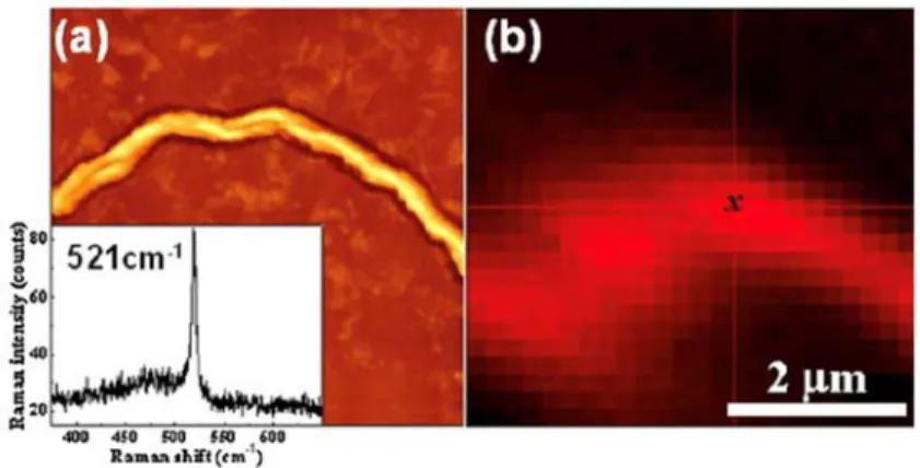
The crystallinity was examined by Raman analysis and the result is shown in Fig. 18. A SiNW segment was visualized by AFM in Fig. 18(a) and corresponding Raman signal intensity was targeting at the same region of SiNW in Fig. 18(b). From the inset in Fig. 18(a), a clear peak centered at 521 cm-1 confirms good crystallinity of the SiNW, which therefore implies the
feasibility of this crystallization technique.
Fig. 18. (a) AFM image of a single SiNW with vertical scale from black to white of 160 nm, and (b) its corresponding crystalline Si Raman peak signal mapping (integrated in the spectral
window 521±5 cm-1). The inset in (a) shows the Raman spectrum recorded from the position marked with an x in (b) [40].
The mechanism of crystallization of a-Si as well as growth of SiNWs is well explained in [40], [41]. At the early phase of crystallization, when temperature exceeds the eutectic temperature of indium (~157 ˚C), the indium drops turn into liquid state and begin to absorb
silicon seeds would happen in In drops. Since there is a difference of Gibbs energy between a-Si and c-a-Si, the crystallization would continue under the driving force generated from the difference.
Fig. 19. Three SiNWs (A, B, and C) obtained on the same sample but with different morphologies [40].
The in-plane SLS grown SiNWs normally have three forms which are shown in Fig. 19 noted as SiNW_A, B and C. SiNW_A and B could be easily distinguished by the real thickness of a-Si absorbed into In drops during crystallization. When all thickness of a-Si is absorbed, the SiNWs tend to grow as zig-zag wires, whereas the SiNWs grow straighter when the real absorbed thickness of a-Si is less than total thickness of a-Si. Specifically, when speed of precipitation of crystallized silicon is faster than the absorption of a-Si, the In drops could be stretched when they move, thus produce even straighter nanowires than the case of SiNW_B. This is the exact case of SiNW_C shown in the inset of Fig. 19. An irregular growth type of SiNWs called suspended growth is discussed in detail in [42], which could help researcher understand better on the growth mechanism of In Plane-SLS (IPSLS) SiNWs. In addition, the size of SiNW is proportional to the diameter of In drop.
In conclusion, crystallization of a-Si could be accomplished by using indium as catalyst. The low eutectic temperature of indium enables lower temperature crystallization compared to the other metal materials.
1.3.4 Other approaches
Beside the low temperature compatible crystallization techniques we reviewed above, there are some other approaches of a-Si low temperature crystallization techniques. They all show a good compromise between the thermal budget and the electrical properties. Here we review four approaches of crystallization such as excimer laser annealing (ELA) [23], [43]–[45], hydrogen induced crystallization [26], [46], carbon nanotube electron beam crystallization (C-beam crystallization) [47] and blue laser annealing (BLA) [48]–[50].
Excimer Laser Annealing (ELA)
Excimer laser annealing is another mature technology to crystallize amorphous silicon by injecting excimer laser shots onto the surface of amorphous silicon. This technology has been broadly researched and has improved and matured over the past 30 years [23].
Typical excimer lasers operate in pulse mode, at frequencies around 300 Hz, with pulse duration in the range of 10-50 ns. The energy output of excimer lasers for fabricating TFTs is in the order of 0.6-2 J. In prior to all the parameters in ELA, pulse-to-pulse repeatability of the excimer laser is the most important manner of the process, and followed by the discharge frequency, output energy and pulse duration.
In general, the energy of one shot of excimer laser is enough to melt silicon at the surface, but the most extreme heating is confined to the near region of the amorphous layer due to the short duration of the laser pulse. As a result, the total integrated energy is generally small since only a small depth of material is processed. Therefore, although the laser pulse can melt a-Si, temperature into the underlying layer that risen by laser is no more than a few hundred degrees [43].
Previously in our lab, T. Pier et al. developed excimer laser crystallization on μc-Si to improve its crystallinity [44]. 200 nm thick μc-Si film was deposited by PECVD on PEN substrate with highest temperature of 165 ˚C. After that, the μc-Si was laser annealed by a pulsed KrF excimer laser emitting at 248 nm. To prevent abrupt hydrogen evolution from the silicon layer leading to μc -Si film destruction, the annealing energy started from 80 mJ/cm2
and increased with a step of 5 mJ/cm2.
From Fig. 20 we can see grain size of silicon has increasingly enlarged after performing ELC with energy of 180 mJ/cm2. Highest grain size is around 100 nm. According to T. Pier’s
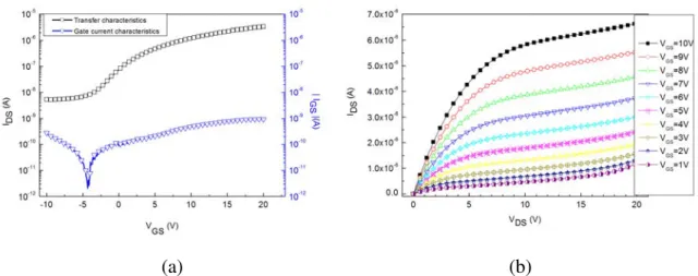
work, energy larger than 180 mJ/cm2 would destroy the PEN substrate. The TFTs based on
annealed and non-annealed μc -Si have been fabricated. The transfer characteristics have been extracted for both cases and are shown in Fig. 21. From this figure we can see the field effect mobility has been seeing a huge improvement from 1 to 46 cm2/V.s after crystallization. In
addition, the off current also increased as expected.
Fig. 20. SEM observation of (a) starting μc -Si film deposited on PEN and (b) after laser annealing at a maximum laser energy of 180 mJ/cm2 [44].
Fig. 21. Transfer characteristics of two same size TFTs (W/L = 40/60) on the same PEN plate produced from starting lc-Si (full line) and lc-Si annealed at a maximum laser energy of
![Table 1. Range of experimental conditions and film properties of amorphous silicon [5]](https://thumb-eu.123doks.com/thumbv2/123doknet/7774107.257395/25.892.107.791.771.1151/table-range-experimental-conditions-film-properties-amorphous-silicon.webp)

![Table 7. The growth rate, optical band gap and mobility-lifetime product of deposited a-Si:H as a function of deposition temperature [21]](https://thumb-eu.123doks.com/thumbv2/123doknet/7774107.257395/34.892.107.787.524.696/optical-mobility-lifetime-product-deposited-function-deposition-temperature.webp)

![Fig. 12. SEM images of fabricated poly-Si films annealed at (a)300 ˚C, (b)350 ˚C, (c)400 ˚C and (d)450 ˚C [33]](https://thumb-eu.123doks.com/thumbv2/123doknet/7774107.257395/40.892.255.641.348.679/fig-sem-images-fabricated-poly-si-films-annealed.webp)
![Fig. 24. TFT mobility as a function of poly-Si grain size [23].](https://thumb-eu.123doks.com/thumbv2/123doknet/7774107.257395/50.892.277.605.717.994/fig-tft-mobility-function-poly-si-grain-size.webp)

![Fig. 33. Schematic of ICP-CVD system [53].](https://thumb-eu.123doks.com/thumbv2/123doknet/7774107.257395/61.892.230.658.579.890/fig-schematic-of-icp-cvd-system.webp)
