HAL Id: hal-00864932
https://hal.archives-ouvertes.fr/hal-00864932
Submitted on 23 Sep 2013
HAL is a multi-disciplinary open access
archive for the deposit and dissemination of
sci-entific research documents, whether they are
pub-lished or not. The documents may come from
teaching and research institutions in France or
abroad, or from public or private research centers.
L’archive ouverte pluridisciplinaire HAL, est
destinée au dépôt et à la diffusion de documents
scientifiques de niveau recherche, publiés ou non,
émanant des établissements d’enseignement et de
recherche français ou étrangers, des laboratoires
publics ou privés.
Influence of secondary phases during annealing on
re-crystallization of CuInSe2 electrodeposited films
A. Gobeaut, Lydia Laffont, Jean-marie Tarascon, L. Parissi, O. Kerrec
To cite this version:
A. Gobeaut, Lydia Laffont, Jean-marie Tarascon, L. Parissi, O. Kerrec. Influence of secondary phases
during annealing on re-crystallization of CuInSe2 electrodeposited films. Thin Solid Films, Elsevier,
2009, vol. 517, pp. 4436-4442. �10.1016/j.tsf.2009.01.043�. �hal-00864932�
O
pen
A
rchive
T
OULOUSE
A
rchive
O
uverte (
OATAO
)
OATAO is an open access repository that collects the work of Toulouse researchers and
makes it freely available over the web where possible.
This is an author-deposited version published in :
http://oatao.univ-toulouse.fr/
Eprints ID : 8665
To link to this article : doi:10.1016/j.tsf.2009.01.043
URL :
http://dx.doi.org/10.1016/j.tsf.2009.01.043
To cite this version : Gobeaut, A. and Laffont, Lydia and Tarascon,
Jean-Marie and Parissi, L. and Kerrec, O. Influence of secondary
phases during annealing on re-crystallization of CuInSe2
electrodeposited films. (2009) Thin Solid Films, 517 (15). pp.
4436-4442. ISSN 0040-6090
Any correspondance concerning this service should be sent to the repository
administrator:
staff-oatao@listes-diff.inp-toulouse.fr
Influence of secondary phases during annealing on re-crystallization of CuInSe2
electrodeposited films
A. Gobeaut
a, L. Laffont
a,⁎
, J.-M. Tarascon
a, L. Parissi
b, O. Kerrec
baLaboratoire de Réactivité et Chimie des Solides, 33 rue St Leu, 80039 Amiens, France
bInstitut de Recherche et de Développement de l’Energie Photovoltaïque, 6 quai Watier, 78401 Chatou cedex, France
Keywords: Solar cells Electrodeposition
Scanning electron microscopy Transmission electron microscopy X-ray diffraction
Electrodeposited CuInSe2thin films are of potential importance, as light absorber material, in the next
generation of photovoltaic cells as long as we can optimize their annealing process to obtain dense and highly crystalline films. The intent of this study was to gain a basic understanding of the key experimental parameters governing the structural–textural-composition evolution of thin films as function of the annealing temperature via X-ray diffraction, scanning/transmission electron microscopy and thermal analysis measurements. The crystallization of the electrodeposited CuInSe2films, with the presence of Se and
orthorhombic Cu2− xSe (o-Cu2− xSe) phases, occurs over two distinct temperature ranges, between 220 °C
and 250 °C and beyond 520 °C. Such domains of temperature are consistent with the melting of elemental Se and the binary CuSe phase, respectively. The CuSe phase forming during annealing results from the reaction between the two secondary species o-Cu2− xSe and Se (o-Cu2− xSe +Se →2 CuSe) but can be decomposed
into the cubic β-Cu2− xSe phase by slowing down the heating rate. Formation of liquid CuSe beyond 520°C
seems to govern both the grain size of the films and the porosity of the substrate–CuInSe2film interface. A
simple model explaining the competitive interplay between the film crystallinity and the interface porosity is proposed, aiming at an improved protocol based on temperature range, which will enable to enhance the film crystalline nature while limiting the interface porosity.
1. Introduction
Silicon solar cells are still strongly leading the photovoltaic (PV) market with more than nine out of ten produced cells. Nevertheless, production of crystalline silicon is not important enough to meet the constantly growing demands from the industry. Such a shortage resulted in an important increase in the silicon price and contributed to a resurged interest in non-silicon thin film cells. Moreover, a common target for all PV industrials is to reduce the production costs while keeping decent efficiency. This proved to be successful as witnessed by the arrival of the second generation of thin film solar cells, which provide drastic improvements in terms of cost-efficiency and yields[1]. For non-silicon thin film cells, chalcopyrite compounds Cu(InxGa1− x)(SeyS1− y)
seem to be the most promising material owing to their low cost and high efficiency yields in laboratory prototypes. Yields ranging from 12% for large-scale modules (4000 cm2) to 19.9% for small-area devices[2]were
achieved. Furthermore, Cu(InxGa1− x)(Sey) modules have been
pro-duced on an industrial scale[3–4]via physical deposition processes that require high vacuum conditions resulting in high production costs. Usually, they are made by deposition of stacked elemental layers (SEL method) of Cu/In(Ga)/Se(S) via co-evaporation or sputtering of Cu and
In metallic elements followed by selenization and/or sulfurization by rapid thermal annealing leading to cells with about 12% efficiencies (Shell Solar Process)[5].
An attractive alternative approach is the two-step electrodeposi-tion–annealing process. By slightly deviating from this process, a few laboratories have increased the material efficiency. The National Renewable Energy Laboratory (Department of Energy, U.S.A.) has, for instance, added an In co-evaporation step (or/and Ga) to the process prior to annealing in order to adjust the stoichiometry of the films with the best results being the achievement of 15.4% cell efficiency[6]
at a slightly higher cost owing to the extra processing step. Recently, Jost et al., working with Atotech GmbH, performed electrodeposited precursors leading to similar reaction path as obtained in the case of the physical vapour deposition SEL method[7]. The process consists in depositing a very low amount of Se onto the precursor film during electrodeposition (Se/In ratio equal to 0.1), so as to obtain copper/ indium binary phases (Cu11In9and CuIn2). By doing so, the CuInSe2
(CISe) phase cannot be formed during the electrodeposition step but is later obtained during an annealing step carried under Se atmosphere. With this process, the binary selenide phases are formed beyond the selenium melting point (221 °C). After selenium transfer reactions, Cu2− xSe and InSe are obtained, and according to the authors, these
two phases react upon annealing with the elemental Se to form CuInSe2
(Cu2− xSe+2InSe+Se→2 CuInSe2) [7]. In our case, the project,
⁎ Corresponding author. Tel.: +33 3 22 82 79 01; fax: +33 3 22 82 75 90. E-mail address:lydia.laffont@u-picardie.fr(L. Laffont).
named CISEL meaning “CuInSe2by Electrodeposition”, consists in a
two-step electrodeposition–flash annealing process without any vacuum restriction in order to strongly reduce the production costs of CuInS2
absorbers. The versatility of this process further relies on the fact that sulfurization of the absorber is performed during annealing by previously adding a sulphur layer on the surface of the ED CuInSe2
precursors via chemical bath deposition.
Precisely, the electrodeposition step is achieved on soda lime glass–Mo substrate, and directly leads to the growth of CuInSe2films;
the latter mainly consist of the ternary chalcopyrite CISe phase toge-ther with elemental Se and Cu–Se binaries compounds. The obtained films have a low crystallinity, and secondary species are present in the entire bulk; so an annealing step is necessary after electrodeposi-tion and chemical vaporizaelectrodeposi-tion of sulphur on it in order to obtain films having the expected semi-conductive properties. This results in an important increase in the grains size together with the random apparition of a huge porosity near the CISeS–substrate interface that is absolutely harmful to the cells efficiency. Despite this, a cell has been made with a record efficiency of 11.3%[8], although, in order to master the porosity issue, all the mechanisms leading to the recrystallization of the films during the annealing step have to be well understood. Although a great deal of study has been done by various groups regarding the film recrystallization mechanism and the interplay between the crystalline nature of the film and its porosity, some of the fundamentals remain unknown. Hence our motivation for this thorough study that will mainly focus on the temperature-driven structural/morphology evolution of the secondary phases present in the as-made electrodeposited films. So, in order to limit the para-meters of the system, the sulfurization of the precursors will not be taken into account in this study. This paper will be organized as follows: in the first part, the morphology and composition of the electrodeposited (ED) precursor will be determined and correlated with “in situ” thermal analyses; then the recrystallization of this precursor will be studied by analysis of different annealed samples, and finally a recrystallization mechanism depending on the heating rate will be put forward for ED CuInSe2films.
2. Experimental details 2.1. Film growing process 2.1.1. Electrodeposition
One single electrodeposition step was enough to grow the CISe precursors in an acidic bath containing Cu(II), In(III) and Se(IV) electroactive species. These CISe films were deposited on Mo-coated soda-lime glass. The reaction of CISe formation at the cathode is described elsewhere [8]. According to thermodynamic considera-tions, similar secondary phases often coexist with the main CISe phase
[9–10]. After electrodeposition, films are recovered from the electro-lytic bath, and dried with N2prior to being annealed. The ED process is
performed either on 5 ×5 cm2or 30× 30 cm2substrates using two
different electrolysers. 2.1.2. Annealing
A rapid thermal process is performed in a customized halogen lamp furnace. The samples are placed onto a graphite susceptor covered with a quartz lid in order to keep a pressure of Se during annealing. The furnace is evacuated and purged with argon flow. The temperature of the process is determined using a thermocouple and a pyrometer placed above the graphite susceptor.
2.2. Characterization 2.2.1. XRD
X-Ray powder diffraction (XRD) patterns of the films were collected on a Scintag Diffractometer using a Cu Kα radiation
operating at 40 kV–40 mA in the range 2θ=20–60° with a 2θ step size of 0.06°. The temperature structural evolution of the ED films was followed by in situ XRD using a Brucker D8 Diffractometer with the CoKα radiation (λ1=1.78919 Å, λ2=1.79321 Å), operating at 30 mV–
40 mA in the 2θ =20–70° range with a 2θ step size of 0.015°, equipped with a Gobel mirror and a Braun PSD collector. The samples were heated in an Anton Parr Chamber HTK using a nitrogen flow, and each XRD pattern was recorded every 25 °C. The ED sample had to be prepared to fit the sample holder within the chamber of the furnace; it was cut into a 1 cm2badge, and a diamond wire reduced the thickness
of the glass substrate down to 0.8 mm. 2.2.2. SEM/TEM
Scanning electron microscopy (SEM) images of the film were recorded using a FEI Quanta FEG operating at 20 kV in order to study the films morphology. Transmission electron microscopy (TEM) study was carried out with an analytical FEI Tecnai F20 ST microscope operating at 200 kV and equipped with an Energy Dispersive Spectroscopy (EDS) analysis. Samples for electron microscopy studies were prepared by scratching the surface of the films and depositing the result onto a nickel grid coated with lacey-carbon film. The electron diffraction patterns were performed using the selected area electron diffraction (SAED) mode.
2.2.3. Calorimetry
Differential Scanning Calorimetry (DSC) analysis was performed on a Phoenix DSC 204 F1 set up manufactured by Netzsch. For such measurements, thin films were scratched to get the powder. The latter was inserted into an alumina crucible that was then sealed under argon atmosphere for measurement. The sample temperature was calibrated using the onset of the melting of both tin (Tm= 231.88 °C) and indium (Tm= 156.6 °C) with a heating rate of
qh= +10 °C min− 1. DSC experiments were systematically carried out
over temperatures ranging from 20 °C to 550 °C with a heating rate of qh= +10 °C min− 1. The heat flow was calibrated with the heat fusion
of indium (ΔH = 28.45 J g− 1).
3. Results and discussion 3.1. Electrodeposited precursors
The as-made electrodeposited films were characterized in order to determine their composition, structural characteristics and physical properties. XRD analysis of ED precursors leads to the diffractogram reported inFig. 1a. On both sides of the molybdenum peak located at 40.6° (PCPDF file n° 42-1120, principal orientation (110)), there are three main Bragg peaks located in 2θ angles at 26.6°, 44.3° and 52.4°, which correspond to the (112), (220) and (312) planes of the CuInSe2
chalcopyrite structure (PCPDF file n° 40-1487), respectively[11]. More-over, the extra Bragg peak, represented by a shoulder near the most intensive peak of CISe at 25.4° corresponds to a second phase, iden-tified by the PCPDF file n° 47-1448 as Cu2Sex, but which is more
com-monly reported in the literature as orthorhombic Cu2− xSe (o-Cu2− xSe
in this paper)[12]. Besides, analysis by Raman Spectroscopy performed on ED films showed the presence of elemental selenium in agreement with previous reports[13–14]. Consequently, after electrodeposition, the films not only contain the CuInSe2 phase but also one
crystallized binary phase o-Cu2− xSe and some elemental selenium.
The microstructure of the electrodeposited films, as deduced from SEM measurements (Fig.1b), is typical of the electrodeposited CuInSe2
films as already reported[15,16,17]regardless of both the substrate size (5×5 cm2or 30×30 cm2) and the spotting shots (centre vs. edge of the
substrates). The films are relatively porous with the presence of some spherical clusters (2–3 nm) at their surface; some of them being agglomerated leading to the typical cauliflower shape. Cross-section images of these films (Fig. 1c) indicate that the porosity is essentially
located on the last 200–300 nm of the sample surface, whereas no porosity is present in the bulk of the film that is quite dense with a dendritic growth shape. Moreover, we have noted (Fig. 1d) the appearance of platelets covering parts of the surface of the films when 5×5 cm2electrodeposited films were aged in ambient
atmo-sphere for several weeks. Interestingly, no extra XRD peak associated to these platelets could be obtained for these samples. Therefore to grasp further information on the structural/composition nature of these platelets, complementary TEM and EDS analyses were under-taken. From the SAED pattern (not shown here) we could identify the platelets as the binary phase CuSe, which composition was also confirmed by EDS analysis (ratio Cu/Se equal to 1). The CuSe phase is hexagonal at room temperature (α-CuSe), but undergoes a structural transition into orthorhombic β-CuSe at 48 °C, and converts back to a hexagonal packing at 120 °C (γ-CuSe)[18]. For instance, we noticed that the sample ageing appears after a shorter time for the 5× 5 cm2ED
samples than for the 30 ×30 cm2. Since the appearance of the CuSe
platelets even occurs under nitrogen or vacuum storage conditions, it is suggested that its growth mechanism enlists a reaction between elemental Se and copper-rich binary o-Cu2− xSe phase to give CuSe
platelets (o-Cu2− xSe+ Se →2 CuSe). A great deal of study has already
taken place in our group on the outcome of such phases upon annealing. Further studies on the influence of these two secondary phases (o-Cu2− xSe+ elemental Se) on the recrystallization process of
our electrodeposited CISe films upon heating were performed. Our ED CISe films were annealed then studied by electron microscopy, X-Ray Diffraction, and thermal analysis in the hope of correlating morphol-ogy and phases transitions in order to fully decipher the recrystalliza-tion mechanism.
3.2. Thermal evolution of ED precursors
The thermal evolution of an ED precursor sample (recovered from a 5×5 cm2ED plate) was first studied by in situ XRD as reported in
Fig. 2a. X-Ray diffractograms were collected every 25 °C, and the temperature of the sample was raised to a heating rate of 6 °C/min between each analysis from ambient to 550 °C. For reasons of clarity, only four characteristic diffractograms are reported inFig. 2a.
Regarding the composition evolution of the phases, the XRD pat-tern of the ED CISe precursor sample, having extra peaks corres-ponding to o-Cu2− xSe impurity, does not significantly vary until
200 °C. Therefore, for annealing temperatures greater than 200 °C, the o-Cu2− xSe shoulder signal intensity progressively decreases to totally
disappear near 250 °C (Fig. 2a). No phase other than CISe was detected until 450 °C, maximum temperature prior to the sample deterioration. Indeed, at higher temperatures, our data was not exploitable owing to some leakage in our high temperature chamber resulting in the for-mation of In2O3and MoO2as shown on the 550 °C diffractogram.
Further insight into the crystalline nature evolution of the ED films has been obtained by plotting the variation of the crystallites size ((as deduced from the Sherrer equation using the full width at half maximum (FWHM) of the most intense CISe peak (112)) as function of temperature (Fig. 2b). Attempts to use the Williamson and Hall method to separate size from strain contributions could not be applied here owing to the two sets [(220), (204) and (312), (116)] of overlapping Bragg peaks within the CISe XRD pattern. Regardless of such a difficulty, we noticed in this figure a drastic increase in the crystalline nature of the ED film between 220 °C and 250 °C, corresponding to
Fig. 2. (a) In situ XRD analysis on the ED precursor at 50 °C, 200 °C, 250 °C, and 550 °C partially oxidized; (b) in situ analysis: crystallite size from ED film as function of temperature.
Fig. 1. (a) XRD diffractogram of electrodeposited precursor samples, (b) surface, (c) cross-section SEM pictures of an ‘as-made’ precursor, and (d) SEM picture of a three weeks aged ED film, the surface is completely covered with CuSe platelets.
the disappearance of the o-Cu2− xSe signal in XRD, and also consistent
with the melting temperature of elemental Se (theoretical melting point: 221 °C) present in the precursor. Although we faced inherent experimental problems of oxidation for temperatures greater than 450 °C, such an experiment had the merit of unambiguously indicating the occurrence of a first re-crystallization step taking place on our ED films between 220–250 °C, which coincides with the melting temperature range of elemental Se (e.g.; presence of a liquid phase).
At this point, we followed, via in situ high temperature X-ray diffraction, the chemical reactivity of the secondary o-Cu2− xSe phases
and elemental Se in absence of CISe. This was done to precisely study the thermal evolution of the secondary phases present in the ED film without the presence of the CISe phase.
So, orthorhombic Cu2− xSe has been synthesized using the same
process as Haram et al.[12], which consists in putting a copper piece in an H2SeO3solution (0.1 N). A black powdery thin layer is obtained,
scrapped and then mixed with elemental selenium with a ratio 1/1 corresponding to the ratio determined by Raman Spectroscopy[13–14]
in ED precursors films. Four diffractograms representing the main evolution steps of the phases are reported inFig. 3. Their evolution can be described as follows:
- From 50 °C to 150 °C, the o-Cu2− xSe and elemental Se Bragg peaks
progressively decrease while extra peaks corresponding to the CuSe phase appear.
- From 150 °C to 250 °C, the o-Cu2− xSe and Se peaks totally
disappear to the expense of both intense CuSe peaks and weak peaks corresponding to CuSe2.
- Finally, heating above 250 °C results in the total disappearance of the CuSe2weak peaks together with a decrease in intensity of the
CuSe ones because of the loss of selenium. Between 275 °C and 300 °C, all CuSe peaks have totally disappeared leading to the single cubic phase that could be either Cu1.8Se or Cu2Se. Owing to both
temperature dilatation issues and small lattice parameter differ-ences between cubic Cu1.8Se (PCPDF file n° 71-0044; a=5.765 Å)
and cubic Cu2Se (PCPDF File n° 02-1275, a=5.731 Å), we will from
now on refer to this 300 °C phase as the β-Cu2− xSe with 0b×b0.2
(PCPDF file n° 06-0680, a=5.739 Å), in agreement with the Cu/Se phase diagram[19].
Overall, from in situ XRD, we validated the chemical reactivity of o-Cu2− xSe and elemental Se to lead to the CuSe phase. Moreover, the
formation of this phase starts at low temperature (from 75 °C appearance of peaks of CuSe from XRD). In light of this observation we can conclude that the appearance of CuSe platelets on ED precursors after ageing is due to the low temperature reactivity of o-Cu2− xSe
with Se. Besides, we also spotted at higher temperature (N250 °C) the growth of β-Cu2− xSe phase resulting from the decomposition of the
CuSe phase associated to the loss of Se.
To further support the above scenario, DSC measurements were performed on powders resulting from scratching one 30 ×30 cm2
electrodeposited precursor film. Four main defined peaks correspond-ing to endothermic processes are observed (Fig. 4a). The first one (denoted (i)) although shifted from 221 °C to 255 °C is most likely due to elemental selenium trapped within the CISe films. Interestingly, for comparison, DSC analysis of 5× 5 cm2samples shows no shift of the Se
melting peak (Fig. 4b). This difference in thermal behaviour could also account for the differences in ageing behaviour observed for 30× 30 cm2 and 5× 5 cm2 samples; knowing from our experience
that the electrodeposition step leads to more free elemental selenium in the case of the smallest samples than for the 30 ×30 cm2ones.
Furthermore, the weak intensity of the Se melting peak for the 5×5 cm2powder can be explained by its easier partial consumption
due to the formation of CuSe as previously shown from in situ XRD. So, the more accessible elemental Se is, the easiest it is to form CuSe; this
Fig. 3. In situ XRD analysis of o-Cu2− xSe mixed with elemental selenium, at 50 °C,
150 °C, 250 °C and 300 °C.
Fig. 4. (a) DSC thermogram from ED precursor powder obtained by scratching films: (i): 255 °C: Se melting (shifted), (ii): 340 °C: CuSe2→ CuSe + Se(liq), (iii): 380 °C: CuSe →β-Cu2− xSe +Se(liq), (iv): 521 °C: CuSe melting (b) DSC analysis of powder
explains the differences in intensity of the Se melting endothermic peak between the 5×5 cm2and 30 ×30 cm2samples.
Going back to the DSC analysis, a few endothermic peaks are ob-served at higher temperatures, with namely a second one (ii) at 340 °C due to the decomposition of CuSe2((ii): CuSe2→ CuSe + Seliq.), and a
third one (iii) at 380 °C associated to the CuSe partial decomposition following the reaction 2CuSe→β-Cu2− xSe+Seliq. [20]; this agrees
with our previous in situ XRD measurements, which have shown the growth of β-Cu2− xSe between 275 °C and 300 °C (Fig. 3). These two
reactions lead to the formation of liquid Se which could benefit the CISe re-crystallization by acting as a constant flux.
Finally, the last endothermic peak near 521 °C corresponds to CuSe melting (theoretical melting point: 524 °C[19]). However, it should be mentioned that the DSC analysis is carried out in a sealed crucible, meaning that no loss of selenium occurs whereas in an open space the decomposition of the CuSe phase is irreversible due to the loss of selenium during the process. This implies that the decomposition of CuSe would lead to the formation of β-Cu2− xSe. So, the [Cu2− xSe]/
[CuSe] ratio in a sample heated above 380 °C is strongly dependent on the heating rate. The slower the heating rate is, the more β-Cu2− xSe
will be formed. Furthermore, this β-Cu2− xSe phase has a high melting
point of 1113 °C, which would be unreachable for our process, meaning that this phase would stay trapped in the bulk in the solid state and could not participate in the increase in the CISe grain size. So, a fast annealing ramp is necessary to re-crystallize the sample in order to avoid a loss of selenium in the copper–selenide binary compounds, and to keep the CuSe phase in the film till its melting point at 524 °C (Fig. 4b).
Last, we should mention the existence of an extra endothermic peak, near 480 °C, which cannot be accounted with respect to the phase transitions supposed to occur in our system. In light of the In–Se binary phases diagram[19], a possible reaction to explain this extra peak would be the fusion of In3Se4occurring near 500 °C, but XRD
analysis have been unsuccessful to support this hypothesis. 3.3. Annealed samples
To check the informations deduced from the aforementioned in situ analyses of the ED precursors, an ex situ study of samples annealed on the halogen lamps furnace was undertaken. 2.5 ×2.5 cm2
sample specimens cut out of a 30 ×30 cm2ED sample were annealed
according to the following temperature protocol: it consists of a
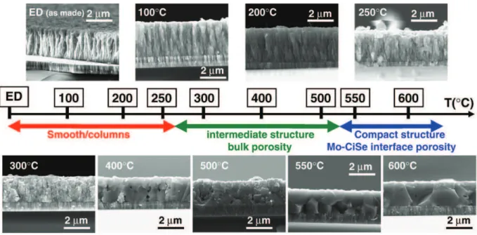
heating ramp of 2 min to various temperatures ranging from 100 °C to 600 °C followed by a 10 min annealing step at the selected temperature. Afterwards, the cross-section of the resulting annealed samples was observed by SEM (Fig. 5). The collected SEM images show the temperature-driven thin film morphology evolution that can be classified in three categories; each corresponding to a specific annealing temperature range.
- For annealing temperatures up to 250 °C, the columnar structure of the ED CISe thin films is preserved.
- Annealing treatments ranging from 300 to 500 °C lead to an intermediate film structure with the presence of porosity both at the surface and in the bulk of the film. While the sample annealed at 300 °C is quite porous, samples annealed at higher temperatures (400 °C and 500 °C) present larger particle sizes and are denser, but still contain porosity within their core.
- Finally, further annealing to 550 °C and 600 °C results in compact films having therefore some porosity essentially located near the Mo–CISe interface.
Additionally, hexagonal-shaped crystals were observed on the surface of the samples annealed between 100 °C–300 °C (Fig. 6a —SEM picture), and analyzed by TEM (Fig. 6b). From the selected area electron diffraction pattern (Fig. 6c) we could deduce that these crystals correspond to the γ-CuSe phase (PCPDF file n° 27-0185) in
Fig. 5. SEM cross-section pictures from ED precursors annealed at different temperatures (heating with a step of 10 min reached with a 2 min heating ramp for each temperature).
Fig. 6. (a) SEM picture of 330 °C annealed sample surface showing the presence of CuSe crystals; (b) Bright field TEM picture, and (c) SAED pattern of one CuSe crystal.
agreement with EDS analysis that has revealed a Cu/Se ratio of 1, and consistent with DSC measurements that have shown that the CuSe phase does not decompose until 380 °C.
The annealed samples were also studied by XRD, and their diffractograms are reported inFig. 7a. The shoulder at 25.4°, located near the (112) CISe principal peak and corresponding to the binary o-Cu2− xSe phases observed on ED precursors, is still present until
250 °C, but vanishes at higher temperatures concomitantly with a sharpening of the main Bragg peaks corresponding to the CISe phase. Although SEM has revealed the presence of CuSe crystals, no extra peak due to the CuSe phase could be detected, implying that the formation of CuSe on the surface is very localized and punctual. In order to qualitatively track the temperature-driven crystalline evolution of our samples, the FWHM of the principal CISe peak (26.6°, (112) plane) was determined for each annealed sample and plotted inFig. 7b. Although we are well aware that caution should be exercised in over-interpreting such Bragg peak widths, which also depend on particle size and strains, we can deduce with full confidence that, like for the morphology, the crystalline evolution of the samples upon annealing is step-wise with the most prominent increase being observed for annealing
tempera-tures ranging from 250 °C to 300 °C. The onset of such a crystallite coarsening in this temperature domain nicely fits with the melting of Se that was shown to occur near 250 °C, as deduced by DSC (Fig. 4a), for a 30×30 cm2sample. Finally, no noticeable changes in the
coarse-ning of the particles were revealed for annealing temperatures greater than 300 °C. In contrast a spectacular morphology change, leading to massive grains (e.g., material densification), was observed between 500 and 550 °C. This range of temperatures can obviously be related to the melting of CuSe occurring at 524 °C.
3.4. Recrystallization mechanism
The above results have shown that the crystallinity and morphol-ogy of the CISe ED precursors containing o-Cu2− xSe and elemental Se
phases can be tuned over two well-determined domains of tempera-ture. The first one from 220 °C to 300 °C, which involves the melting of elemental Se, enables to act on the crystalline nature of the CISe film while the second one, near 520 °C and corresponding to the melting point of CuSe, enables the coarsening and the densification of the main phase. However, some differences were noted in the film crystallinity/morphology evolution depending on the history of the treated film (freshly made vs. aged films) and the type of annealing procedure being used (thermal vs. flash heating). Such an observation directly implies the influence of slow vs. fast annealing on recrystalli-zation of the films as discussed next.
Let's first consider freshly made films:
- For slow annealing rate (Fig. 8a), the melting of Se at 221 °C enables an enhancement of the crystalline nature of the CISe film as proven by the increase in the crystallites size between 230 °C and 250 °C as deduced by “in situ” XRD analysis. But afterwards, owing to the peritectoidic reaction (2CuSe →β-Cu2− xSe+Seliq.)
occurring at 377 °C, the elemental selenium is progressively removed from the film. Consequently, the initial binary phase o-Cu2− xSe, which is transformed into CuSe, then decomposes and
converts into a poor selenide β-Cu2− xSe phase, therefore
preventing the 520 °C grain-coarsening step associated to CuSe. - On the contrary, when annealing is fast, either via Infrared lamps or
operated in closed environment (like in DSC measurements) (Fig. 8b), selenium loss is minimized so that the two successive enhancements of the crystallites and grains size forming the CISe films can occur. The first one, still due to Se melting, enables to enhance the crystallite growth (e.g.; sample crystallinity), while the second one, associated to the melting of the CuSe phase near 521 °C, as deduced from DSC measurements, favours grain coarsening. In short, fast annealing (or closed space annealing) avoids selenium loss of the film so that the CuSe compound is formed and its melting promotes the formation of compact and massive films with the presence of porosity near the Mo–CISe interface.
In contrast with the freshly made films, we have shown that the ageing of CISe leads to the formation of CuSe platelets owing to the chemical reactivity of o-Cu2− xSe with elemental Se at room
temperature. In such a case, as before and even more so when the annealing is too slow, the existing CuSe phase is totally decomposed, and cannot contribute to the enhancement of the grain size observed near 520 °C. Hence the advantage of using a fast rating process for the aged films as well.
All these information enable to suggest the recrystallization mechanism reported onFig. 8distinguishing between slow and fast annealed samples for either freshly made or aged CISe samples. Thanks to this mechanism, we can define a heating protocol involving the two aforementioned liquid phases while producing CISe deposits with minimized porosity. Owing to the greatest conversion yield associated with the presence of sulphur within the CISe films, we are presently revisiting the above mechanism when sulphur is deposited
Fig. 7. (a) XRD of ED precursors annealed at different temperatures (same heating conditions asFig. 5); (b) Full width at half maximum (FWHM) of the (112) main CuSe peak as function of the annealed temperature.
as a thin layer on top of the CISe films or when CISe films are annealed under a sulphur-containing atmosphere.
4. Conclusion
We have reported the influence of the o-Cu2− xSe and Se secondary
phases on the re-crystallization process of ED CISe films. We showed this re-crystallization process to be governed by the existence of two liquid phases (Se at 221 °C and CuSe at 524 °C) that act as a flux to promote crystallite or grain size coarsening, respectively, and whose appearance is strongly dependent on the annealing process. Fast heating, which leads to the successive appearance of the Se and CuSe phases, is preferred to low heating, which solely leads to liquid Se and solid that decompose into β-Cu2− xSe and Se prior to reaching the
CuSe melting temperature. The presence of the liquid Se phase is mandatory to enhance the crystalline nature of the film while the presence of a CuSe liquid film is necessary for an optimization of the grain size, but unfortunately, it comes with an important increase in the porosity near the Mo–CISe interface. Future work will aim to determine the influence of the crystalline nature, grain size and porosity of the ED CISe films on their semi-conductive properties so as to produce CISe solar cells with high conversion yields. Due to the determination of the re-crystallization mechanism, we might be able to both adjust the electrodeposition parameters as well as the heating ramp in order to facilitate the presence of CuSe or β-Cu2− xSe as well.
Acknowledgements
We gratefully acknowledge O. Ramdani, C. Van-de-Putte, P.P. Grand and P. Panheleux from the IRDEP for the synthesis of the electro-deposited precursors and the annealing of the samples. The authors also gratefully acknowledge A. Finke from the LRCS for the differential
scanning calorimetry measurements and the ANR (Allocation Natio-nale de Recherche) for the funds.
References
[1] M.A. Green, Sol. Energy 76 (2004) 3.
[2] I. Repins, M.A. Contreras, B. Egaas, C. Dehart, J. Scharf, C.L. Perlins, B. To, R. Toufi, Prog. Photovolt. Res. Appl. 16 (2008) 235.
[3] M. Powalla, B. Dimmler, Sol. Energy Mater. Sol. Cells 75 (2003) 27. [4] A. Goetzberger, C. Hebling, H.W. Schock, Mater. Sci. Eng. R40 (2003) 1. [5] J. Palm, V. Probst, F.H. Karg, Sol. Energy 77 (2004) 75.
[6] R.N. Bhattacharya, W. Batchelor, K. Ramanathan, M.A. Contreras, T. Moriarty, Sol. Energy Mater. Sol. Cells 63 (2000) 367.
[7] S. Jost, F. Hergert, R. Hock, J. Schulze, A. Kirbs, T. Voβ, M. Purwins, Sol. Energy Mater. Sol. Cells 91 (2007) 1669.
[8] D. Lincot, J.F. Guillemoles, S. Taunier, D. Guimard, J. Sicx-Kurdi, A. Chaumont, O. Roussel, O. Ramdani, C. Hubert, J.P. Fauvarque, N. Bodereau, L. Parissi, P. Panheleux, P. Fanouillere, N. Naghavi, P.P. Grand, M. Benfarah, P. Mogensen, O. Kerrec, Sol. Energy 77 (2004) 725.
[9] L. Thouin, J. Vedel, J. Electrochem. Soc. 142 (1995) 2996.
[10] S. Massaccesi, S. Sanchez, J. Vedel, J. Electrochem. Soc. 140 (1993) 2540. [11] Powder Diffraction File, Joint Committee on Powder Diffraction standards (JCPDS),
ASTM, Philadelphia, PA, 1997.
[12] S.K. Haram, K.S.V. Santhanam, M. Neumann-Spallart, C. Lévy-Clément, Mater. Res. Bull. 27 (1992) 1185.
[13] O. Ramdani, J.F. Guillemoles, D. Lincot, P.P. Grand, E. Chasseing, O. Kerrec, E. Rezpka, Thin Solid Films 515 (2007) 5909.
[14] V. Izquierdo-Roca, A. Pérez-Rodríguez, A. Romano-Rodríguez, J.R. Morante, J. Álvarez-García, L. Calvo-Barrio, V. Bermudez, P.P. Grand, O. Ramdani, L. Parissi, O. Kerrec, J. Appl. Phys. 101 (2007) 103517.
[15] R.P. Raffaelle, T. Potdevin, A.F. Hepp, S.G. Bailey, Mater. Sci. Semicond. Process. 2 (1999) 289.
[16] J. Kois, S. Bereznev, E. Millikov, A. Öpik, Thin Solid Films 511–2 (2006) 420. [17] S. Taunier, J. Sicx-Kurdi, PP. Grand, A. Chomont, O. Ramdani, L. Parissi, P. Panheleux,
N. Naghavi, C. Hubert, M. Ben-Farah, J.P. Fauvarque, J. Connolly, O. Roussel, P. Mogensen, E. Mahé, J.F. Guillemoles, D. Lincot, O. Kerrec, Thin Solid Films 480–1 (2005) 526.
[18] A.L.N. Stevels, F. Jellinek, Recl. Trav. Chim. Pays-Bas 90 (1971) 273. [19] H. Okamoto, J. Phase Equilib. Diffus. 25 (2004) 201.
[20] D. Wolf, G. Müller, Thin Solid Films 361–2 (2000) 155.
Fig. 8. Recrystallization mechanism: for (a) slow annealing and (b) fast (or close space) annealing. The font size illustrates the relative amount of each phase in the film: the larger the font the higher the fraction of that phase in the film. Bold face characters indicates grain size enlargement. The level of crystallinity of the CuInSe2phase is noted by (−) low and (+) high.