A 400GHz f
MAXFully Self-Aligned SiGe:C HBT Architecture
S. Van Huylenbroeck, A. Sibaja-Hernandez, R. Venegas, S. You1, G. Winderickx, D. Radisic, W. Lee, P. Ong, T.
Vandeweyer, N. D. Nguyen, K. De Meyer1 and S. Decoutere IMEC, Kapeldreef 75, B-3001 Leuven, Belgium
1also with K. U. Leuven, ESAT, Kasteelpark Arenberg 10, B-3001 Leuven, Belgium
Abstract
An improved fully self-aligned SiGe:C HBT architecture featuring a single-step epitaxial collector-base process is described. An fMAX value of 400GHz is reached by structural as well as intrinsic advancements made to the
HBT device.
Index Terms : Silicon bipolar process technology, hetero-junction bipolar transistor (HBT), silicon-germanium (SiGe), millimeter-wave bipolar transistor.
I. INTRODUCTION
Continuous improvement of the SiGe:C HBT device performance, reflected by higher current-gain and power-gain cutoff frequencies fT and fMAX,has put this fully Si-manufacturing compatible bipolar transistor on the road for millimeter-wave circuit applications demanding large bandwidth and high data rates in high-speed
communication and radar systems [1-3].
In order to push the HBT performance further into the terahertz operation regime, it is important to scale the device in vertical direction but more essential is the ability to lower the device parasitic elements as much as possible. For this reason, a fully self-aligned SiGe:C HBT architecture based on the growth of the collector-base region in one single epitaxial step was presented in [4]. The removal of the external device regions using a sacrificial emitter pedestal and the self-aligned reconstruction of the base contacts using oxide/poly deposition and CMP planarization techniques enabled the independent reduction of the base resistance and the collector-base capacitance.
In this paper, we describe further improvements to this architecture. We will demonstrate the structural
advancements to the bipolar device and show a better control of the dopant distributions near the base-collector junction. With the upgrade of this fully self-aligned architecture, we are able to demonstrate fMAX value of 400GHz, almost a factor of 2 higher compared to [4].
II.HBTTECHNOLOGYDESCRIPTION
The collector drift region and extrinsic base in this device architecture are made fully self-aligned to the emitter. This paragraph describes how this alignment is achieved.
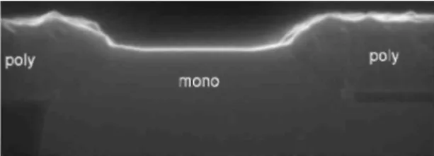
Different to the transistor in [4], the sinker and base active region are now merged. A high dose buried layer module is processed prior to the shallow trench isolation (STI) module. There is no deep trench module (DTI) present in this architecture. A shallow sinker implantation is performed in order to assure a good contact to the collector buried layer. After the deposition of an oxide/nitride seed layer to protect the CMOS regions, these layers are removed from the bipolar active regions. The next step involves the single step non-selective epitaxial deposition of the collector drift region and the SiGe:C base. The total thickness of this layer is around 190nm. This thickness has been chosen such that the subsequent CMP planarization steps are not destroying a CMOS transistor that will be present when integrating this HBT architecture into a CMOS flow. The epitaxial layer obviously grows poly crystalline on the nitride and mono crystalline on the bipolar active (see figure 1 below). The first part of the collector drift region is doped with phosphor at a level around 1e19cm-3. Before growing the
base layer, an undoped Si:C layer is present. This layer will prevent an excessive up diffusion of the phosphorous dopants towards the base, as will be shown later.
Fig. 1. Bipolar device after the single-step epitaxial growth of the collector drift and the base layer.
A nitride pedestal layer is deposited next. This layer acts as a dummy emitter and is patterned together with the underlying silicon after a 193nm DUV light field lithography exposure. The nitride sidewalls are etched almost perfectly vertical (see figure 2), an important improvement compared to the bipolar transistor in [4]. The dry etch into the silicon substrate has been kept better under control by optimizing the endpoint triggering of the etch down to the nitride pedestal layer. All the poly crystalline silicon from the non-selective epitaxially grown layer has been removed.
Fig. 2. Bipolar device after the pedestal etch of nitride and silicon. Width of the nitride = 150nm.
The external base reconstruction module starts with the deposition and planarization of a thick HDP layer. A combination of a well controlled dry oxide etch back step and a short HF dip removes the oxide to a level just below the intrinsic base layer. Next, an in-situ boron doped poly crystalline layer, acting as the external base layer and making contact to the intrinsic base sidewalls, is deposited and planarized as well. This poly layer is dry etched back towards a level about half of the nitride dummy emitter (figure 3), leaving about l00nm external base poly silicon. It is important that the external base poly silicon layer is thick enough, as part of the silicon will be consumed during silicidation. When the external base poly becomes too thin, as was the case in [4], the complete poly layer gets silicided, resulting in an increased base resistance.
Another HDP oxide deposition and planarization step forms an inter-poly oxide between external base and emitter. All CMP steps are kept well under control due to the presence of bipolar dummies on the test chip. The dry etch back steps are all very selective towards the nitride pedestal layer.
Before the deposition of the poly crystalline arsenic in-situ doped emitter, the dummy nitride pedestal is removed and replaced by L-shaped inside spacers. Due to the vertical nitride pedestal sidewalls, the width of these inside spacers can be controlled very well. The effective width of the emitter window is equal to 80nm, for a 150nm designed width.
Published in : IEEE Bipolar/BiCMOS Circuits and Technology Meeting (2009)
Authors : S. Van Huylenbroeck, A. Sibaja-Hernandez, R. Venegas, S. You, G. Winderickx, D. Radisic, W. Lee, P. Ong, T. Vandeweyer, N. D. Nguyen, K. De Meyer and S. Decoutere
Fig. 3. Bipolar device after the poly dry etch back.
silicon from the non-selective epitaxially grown layer has been removed.
Fig. 2. Bipolar device after the pedestal etch of nitride
and silicon. Width of the nitride = 150nm.
The external base reconstruction module starts with the deposition and planarization of a thick HDP layer. A combination of a well controlled dry oxide etch back step and a short HF dip removes the oxide to a level just below the intrinsic base layer. Next, an in-situ boron doped poly crystalline layer, acting as the external base layer and making contact to the intrinsic base sidewalls, is deposited and planarized as well. This poly layer is dry etched back towards a level about half of the nitride dummy emitter (figure 3), leaving about 100nm external base poly silicon. It is important that the external base poly silicon layer is thick enough, as part of the silicon will be consumed during silicidation. When the external base poly becomes too thin, as was the case in [4], the complete poly layer gets silicided, resulting in an increased base resistance.
Another HDP oxide deposition and planarization step forms an inter-poly oxide between external base and emitter. All CMP steps are kept well under control due to the presence of bipolar dummies on the test chip. The dry etch back steps are all very selective towards the nitride pedestal layer.
Fig. 3. Bipolar device after the poly dry etch back.
Before the deposition of the poly crystalline arsenic in-situ doped emitter, the dummy nitride pedestal is removed and replaced by L-shaped inside
spacers. Due to the vertical nitride pedestal sidewalls, the width of these inside spacers can be controlled very well. The effective width of the emitter window is equal to 80nm, for a 150nm designed width.
The bipolar module is finished by the subsequent patterning of the poly emitter and poly base regions. Bipolar spacer formation is done prior to the 1085ºC CMOS compatible junction RTA. Nickel silicide formation and back-end metallization finishes the device (figures 4a & 4b).
Fig. 4a. Bipolar device after end of processing in B-E-C configuration.
Fig. 4b. Zoom in of bipolar device after end of processing. Effective emitter window width = 80nm.
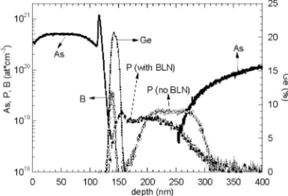
The end of line SIMS profiles of the full HBT device are shown below. The epitaxially grown collector drift region, simultaneously deposited with the base, consists of a phosphorous doped and an undoped part. The latter accommodates the up diffusion of dopants towards the base due to the rapid thermal anneal. In figure 5, the undoped collector part does not contain any carbon. The phosphorous dopants in the presence of an arsenic doped buried layer (BLN) exhibit a pronounced up diffusion and
6
Authorized licensed use limited to: IMEC. Downloaded on August 13,2010 at 08:29:04 UTC from IEEE Xplore. Restrictions apply.
Fig. 4a. Bipolar device after end of processing in B-E-C configuration.
Fig. 4b. Zoom in of bipolar device after end of processing. Effective emitter window width = 80nm.
The bipolar module is finished by the subsequent patterning of the poly emitter and poly base regions. Bipolar spacer formation is done prior to the 1085°C CMOS compatible junction RTA. Nickel silicide formation and back-end metallization finishes the device (figures 4a & 4b).
The end of line SIMS profiles of the full HBT device are shown below. The epitaxially grown collector drift region, simultaneously deposited with the base, consists of a phosphorous doped and an undoped part. The latter accommodates the up diffusion of dopants towards the base due to the rapid thermal anneal. In figure 5, the undoped collector part does not contain any carbon. The phosphorous dopants in the presence of an arsenic doped buried layer (BLN) exhibit a pronounced up diffusion and segregation towards the Si/SiGe collector-base
Published in : IEEE Bipolar/BiCMOS Circuits and Technology Meeting (2009)
Authors : S. Van Huylenbroeck, A. Sibaja-Hernandez, R. Venegas, S. You, G. Winderickx, D. Radisic, W. Lee, P. Ong, T. Vandeweyer, N. D. Nguyen, K. De Meyer and S. Decoutere
interface. This will increase the base-collector capacitance, especially the perimeter component, and therefore deteriorate the RF performance of the HBT device. A way to control the excess phosphorous diffusion due to the presence of the highly doped arsenic layer (BLN) is adding a small amount of carbon (0.2%) to the undoped collector part. Figure 6 shows the end of line SIMS profiles. The up diffusion of the phosphorous towards the base layer is now strongly suppressed. The base-collector capacitance for a 1µm long HBT device could therefore be reduced from 3.4fF to 1.55fF.
Fig. 5. EOF SIMS profiles for transistor with a Si undoped collector region underneath the base.
Fig. 6. EOF SIMS profiles for transistor with a Si:C undoped collector region underneath the base.
III. HBT DEVICEPERFORMANCE
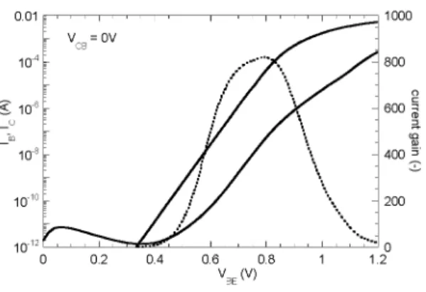
A transistor gummel plot for a 0.15×1.0µm (designed dimensions) HBT device is shown in figure 7. Both the base and collector current ideality are good. The current gain is limited to 800, due to the use of a 2-step Ge-profile (8% and 21% respectively) in the base SiGe:C layer. The emitter-base tunnel current, visible at low VBE
values, is limited as well.
The base-collector reverse diode current, shown in figure 8, demonstrates the influence of the 0.2%) carbon added to the undoped collector part. Because of the limited up diffusion of the phosphorous dopants in that case, the base-collector leakage current is reduced with 4 to 5 orders of magnitude. Obviously, the BVCBO value is
increased and reaches 5.2V.
Published in : IEEE Bipolar/BiCMOS Circuits and Technology Meeting (2009)
Authors : S. Van Huylenbroeck, A. Sibaja-Hernandez, R. Venegas, S. You, G. Winderickx, D. Radisic, W. Lee, P. Ong, T. Vandeweyer, N. D. Nguyen, K. De Meyer and S. Decoutere
Fig. 7. Gummel plot for a 0.15×1.0µm2 HBT device with Si:C collector.
Fig. 8. Base-collector reverse diode current for a 0.15×1.0µm2 HBT device.
Fig. 9. Ic-VCE plot with forced VBE for a 0.15×1.0µm2 HBT device (Si:C collector).
The transistor IC-VCEoutput curves with forced VBE and forced IB respectively are shown in figure 9 and 10.
BVCEO equals 1.7V as can be observed at a forced base current of OA and it can be seen as well for a forced VBE
voltage of 0.7V when base current sign reversal occurs. The early voltage at a VBE value of 0.7V is equal to 60V.
The transistor self-heating, reflected by a negative slope of the collector current as a function of VCE, is limited.
The somewhat smooth transition from the saturation to the active region in figure 10 suggests high injection barrier effects that are not optimized. It might be caused by the presence of a thin undoped collector region underneath the base and will be addressed in future silicon.
Fig. 10. IC-VCE plot with forced IB for a 0.15×1.0µm2 HBT device (Si:C collector).
The fT and fMAXcurves as a function of the collector current are shown in figure 11. The value of fT and fMAXare obtained by extrapolation on the current gain |h21| and unilateral gain |U| curves from the 40GHz measurement point using a -20dB/decade line. The influence of the addition of 0.2% carbon to the undoped collector part is demonstrated.
While the peak fT value remains equal to 215GHz for both cases, the peak fMAXvalue increases from 305GHz to 400GHz due to the decrease of the base-collector capacitance. The collector current at peak performance equals 1.5mA.
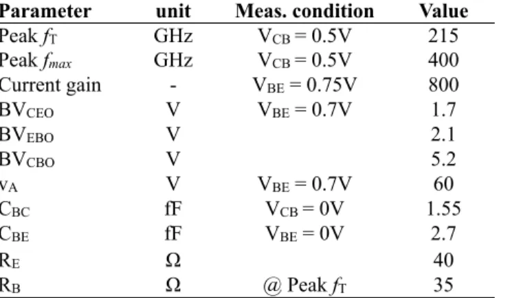
TABLE I ELECTRICAL PARAMETERS FOR A 0.1 5×1.0µM2 HBT DEVICE (Si:C COLLECTOR)
Parameter unit Meas. condition Value
Peak fT GHz VCB = 0.5V 215 Peak fmax GHz VCB = 0.5V 400 Current gain - VBE = 0.75V 800 BVCEO V VBE = 0.7V 1.7 BVEBO V 2.1 BVCBO V 5.2 vA V VBE = 0.7V 60 CBC fF VCB = 0V 1.55 CBE fF VBE = 0V 2.7 RE Ω 40 RB Ω @ Peak fT 35
Fig. 11. fT and fMAXversus Ic for a 0. 15×1.0µm2 HBT.
Published in : IEEE Bipolar/BiCMOS Circuits and Technology Meeting (2009)
Authors : S. Van Huylenbroeck, A. Sibaja-Hernandez, R. Venegas, S. You, G. Winderickx, D. Radisic, W. Lee, P. Ong, T. Vandeweyer, N. D. Nguyen, K. De Meyer and S. Decoutere
The achieved fMAXvalue of 400GHz is also almost a doubling of the value compared to [4]. This improvement is the accumulated results of a further lateral scaling of the HBT device, a significant decrease of the base
resistance and of the base-collector capacitance. Table I summarizes the main DC and AC parameters of the HBT device presented in this paper.
IV. CONCLUSIONS
Improvements to a fully self-aligned SiGe:C HBT architecture, featuring a single-step nonselective epitaxial growth of the collector drift region and the base layer, have been presented. Structural improvements, a further lateral scaling of the HBT device and a better control of the collector dopant distribution resulted in a doubling of the fMAX value for this architecture, now reaching 400GHz.
Acknowledgement
The authors wish to acknowledge the support of the European Commission in the frame of the FP7 IST project DOTFIVE (IST-216110). The authors would also like to thank the IMEC pilot line for processing the wafers. References
[1] A. Fox et al, "SiGe HBT Module with 2.5ps Gate Delay," IEDM Technical Digest, pp. 731-734, 2008.
[2] B. Geynet et al, "SiGe HBTs featuring fT > 400GHz at room temperature," BCTM Proceedings, pp. 121-124, 2008.
[3] J. Yuan et al, "On the Performance Limits of Cryogenically Operated SiGe HBTs and Its Relation to Scaling for Terahertz Speeds," IEEE
Transactions on Electrical Devices, pp. 1007-1019, 2009.
[4] J.J.T.M. Donkers et al, "A Novel Fully Self-Aligned SiGe:C HBT Architecture Featuring a Single-Step Epitaxial Collector-Base Process,"
IEDM Technical Digest, pp. 655-658, 2007. Status : Postprint ( Author’s version)