Université de Québec
Institut National de la Recherche Scientifique Énergie Matériaux Télécommunications
Transparent Conducting Oxides and Multiferroic
Perovskites for Solar Energy Conversion Applications
Wei Huang
Thèse présentée pour l’obtention du grade de Philosophiæ Doctor (Ph.D.) en Sciences de l’énergie et des matériaux
Jury d’évaluation
Président du jury Emanuele Orgiu
et examinateur interne INRS ÉMT
Examinateur externe Jonathan Spanier Drexel University
Examinateur externe Jean-Michel Nunzi Queen’s University
Directeur de recherche Federico Rosei INRS ÉMT Co-directeur de recherche Mohamed Chaker
INRS ÉMT Co-directeur de recherche Riad Nechache
Contents
Abstract ... 1 Acknowledgements ... 6 List of Figures ... 8 List of Tables ... 16 Chapter 1. Introduction ... 17 1.1. Basics ... 171.1.1. Transparent conducting oxides ... 17
1.1.2. Epitaxial thin film ... 19
1.1.3. Perovskite oxides ... 21 1.1.4. Ferroelectricity ... 24 1.1.5. Magnetism ... 26 1.1.6. Multiferroic materials ... 28 1.2. Multiferroic Bi2FeCrO6 ... 30 1.2.1. Synthesis method ... 30
1.2.2. Crystal structure and cationic ordering... 32
1.2.3. Optical properties ... 35
1.2.4. Multiferroic properties ... 37
1.3. Multiferroic materials for solar energy conversion applications ... 40
1.3.1. Photoconductive and photovoltaic effects ... 41
1.3.3. Photocatalytic water splitting ... 49
1.3.4. Multiferroics for solar energy conversion applications ... 53
Chapter 2. Research Objectives and Thesis Organization ... 61
2.1. Research Objectives ... 61
2.2. Thesis organization ... 62
Chapter 3. Experimental Methods ... 65
3.1. Deposition Techniques ... 65
3.1.1. Molecular Beam Epitaxy (MBE) ... 65
3.1.2. Pulsed Laser Deposition (PLD) ... 66
3.1.3. Hybrid Deposition (PLD + MBE) ... 67
3.2. Characterizations ... 68
3.2.1. Characterizations of Thin Films ... 68
3.2.2. Characterizations of Devices ... 70
SECTION I. P-TYPE TRANSPARENT CONDUCTING OXIDES Chapter 4. p-Type Indium-Doped SrTiO3 Thin Films ... 73
4.1. Experimental procedure ... 74
4.2. Structural characterizations ... 75
4.3. Electrical properties ... 80
4.4. Optical properties ... 83
4.5. Summary ... 87 SECTION II. Bi2FeCrO6 FOR SOLAR ENERGY CONVERSION APPLICATIONS
Chapter 5. Switchable Photodiodes based on Epitaxial Bi2FeCrO6 Multiferroic Thin
Films ... 88
5.1. Experimental section... 89
5.2. Characterization of BFCO thin films ... 89
5.3. Current (J)-Electric field (E) analysis ... 91
5.4. J(E) characteristics with FE polarization switching ... 93
5.5. Photoresponse and charge carrier dynamics ... 96
5.6. Summary ... 100
Chapter 6. Multiferroic Bi2FeCrO6 based p-i-n Heterojunction Photovoltaic Devices ... 101
6.1. Experimental section... 102
6.2. Characterizations of BFCO thin films ... 103
6.2.1. Structural characterizations ... 103
6.2.2. Ferroelectric properties ... 106
6.2.3. Optical Properties ... 107
6.3. Characterizations of NiO thin films ... 110
6.4. Photovoltaic performance ... 112
6.5. External quantum efficiency (EQE) ... 116
6.6. Electrochemical Impedance Spectroscopy (EIS) ... 117
6.7. Summary ... 119
Chapter 7. Enhanced Photoelectrochemical Performance in p-Type Transparent Conducting Oxides coated Multiferroic Oxide Thin Films ... 120
7.1. Experimental method ... 121
7.2. Characterizations of BFCO thin films ... 121
7.3. Characterizations of NiO thin films ... 125
7.4. Photoelectrochemical (PEC) performance ... 126
7.4.1. Tailoring PEC performance of the bare BFCO photoelectrodes ... 126
7.4.2. Enhanced PEC performance of photoanodes coated with p-NiO layer ... 132
7.5. Stability and Photon-to-current conversion efficiency ... 135
7.6. Summary ... 138
Chapter 8. Conclusion and Perspectives... 139
8.1. Conclusion ... 139
8.2. Perspectives ... 141
Bibliography ... 143
Appendix A: List of Acronyms ... 157
1
Abstract
Clean and sustainable solar energy is regarded as one of the most reliable and abundant energy sources to replace fossil fuels. To harvest this energy, in the past several decades, the research trend has been towards exploring novel materials and photon-to-electron mechanisms to achieve higher efficiency in solar energy conversion applications, such as photovoltaic (PV) cells. The PV effect is used to directly harvest solar energy by converting the incident photons into following free charge carriers and thus produce electricity. The emerging PV cells mainly differ in how they operate in practice, that is, in the mechanisms that make the sequence of the generation, separation and transport of electronic charge carriers possible. Elucidating those mechanisms is of fundamental importance for understanding the working principle of each solar cell type, and for its further performance optimization. In conventional p-n junction based PV cells, the charge separation is determined by the existence of a gradient in the electrochemical potential, also known as intrinsic built-in electric fields. Moreover, solar-driven water splitting and hydrogen generation technologies that produce hydrogen (H2 gas) and oxygen (O2 gas) by directly decomposing water using an artificial photocatalytic electrode have been extensively studied as a fundamental technology for the future, due to its simplicity, low-cost operation and the use of nearly neutral pH water, such as seawater for large scale solar-fuel production. In the semiconductor photocatalysts, the carrier extraction is no longer limited by thermodynamic diffusion, but the transport of spatially separated electron-hole pairs to the photocatalyst surface is determined by the surface band bending.
2
Ferroelectric (FE) oxides have recently emerged as a new alternative pathway to achieve the separation of photo-generated charge carriers, and their application in photon-to-current (e.g., PV cells, photodetectors) and photoelectrochemical (PEC) devices was recently started to be explored.Since the discovery of PV effect in these materials over 50 years ago, ferroelectric devices including solar cells (FESC) and PEC cells have attracted significant attention owing to many unique advantages. This technology involves a simplified structure and fabrication methods as well as stable and abundant materials. Different from the p-n diode or Schottky diode solar cells, in the FESC, FE polarization plays a dominant role in charge separation and transport. FESC provides reversible directions of photocurrent and photovoltage by polarization direction switching, and also generates above bandgap open-circuit voltages (Voc up to 40 V), which potentially permit to surpass the Shockley-Queisser limit observed in traditional semiconductors cells.
While for a long time such devices were characterized by weak performance values, recent advances led to significant breakthroughs by using multiferroic materials. Multiferroics combine two ferroic functionalities (specifically FE, ferromagnetic or ferroelastic), and typically possess a magnetic order parameter besides the FE one and the electron-electron interaction regulating the magnetic ordering induced a smaller gap (e.g., 2.6–2.7 eV for BiFeO3 and 1.4–2.4 eV for Bi2FeCrO6) than other FE materials (e.g., 3.2–3.6 eV for La–doped Pb(Zr,Ti)O3 and 3.2 eV for BaTiO3). Among these multiferroics, double-perovskite Bi2FeCrO6 (BFCO) is highly promising in PV and photocatalytic applications due to its nontoxicity, chemical stability, narrow bandgap, huge light absorption coefficient (2.5 × 105 cm-1), large
3
remnant polarization (55 µC cm-2 at room temperature (RT)) and magnetization (160 emu cm -3).
A breakthrough in the field of PV and PEC devices occurred through our recent study on multiferroic BFCO epitaxial thin films, which demonstrated a high efficiency solar energy conversion (solar to electrical or chemical energy). In such material, lower band gap and large FE polarization promote an effective charge carrier generation and separation. Single crystalline BFCO with higher ratio of Fe/Cr cation ordering (R≈0.5−5.1%) showed a lower bandgap (Eg≈1.4−1.8 eV) accompanied with weak FE polarization (P≈5−20 µC cm-2), which exhibit thus a semiconductor behavior. In despite of a larger absorption of sun light by semiconducting BFCO films, the weak FE polarization induced internal electric field decreases the separation power of photogenerated carriers and increases the recombination loss. This dramatically affects the performance of the devices. These results clearly suggest a relationship between the optical property, ferroelectricity and crystal structure of BFCO thin films. To advantageously exploit the semiconducting properties of BFCO for PV application, the p-i-n device architectures have to be designed and developed. Here, an intrinsic semiconductor is sandwiched between a heavily doped p- and n-layers. Semiconductor material absorbs a certain portion of the solar spectrum and adjacent layers (electrodes) are required to extract the photo-generated carriers for conveyance to an external electrical load.
The p-type layer in p-i-n devices is possible incident photons enter the intrinsic absorber layer (i-) of the device for conversion into charge carriers. This requires that all other “photo-passive” but functional layers in the PV cell that lie in the path of photons traversing to the absorber should not absorb or back reflect any of the light before it reaches the intrinsic
4
absorber. That is, the window layers must be highly transparent, i.e., having a wider bandgap than the absorber and thus a much lower absorption coefficient in the spectral range of light used for photo-conversion. Electrically, the p-layer should have hole conduction in order to transport the photogenerated holes and block the electrons. Based on these requirements, the
p-type layer in p-i-n devices should be the p-type transparent conducting oxides (p-TCOs).
The work performed in this thesis was therefore driven by two main objectives: (1) synthesis and understanding the fundamental physical properties (i.e., structural, electrical, and optical) of p-TCOs thin films; (2) design and investigating the multiferroic BFCO thin-film absorber based devices for efficient solar energy conversion applications including photodetectors, PV and PEC devices. The results obtained in this work are resumed in two sections as follows:
In the first section, we synthesized the p-type transparent conducting thin films and studied their structural, electrical and optical properties. (1) Perovskite p-type In-doped SrTiO3 (SrInxTi1-xO3 with In concentration in the range 0≤x≤0.15) thin films were grown on LaAlO3 substrates using a pulsed laser deposition (PLD) and molecular beam epitaxy (MBE) combination technique. (2) The In-STO (ISTO, 0.1≤x≤0.15) films grown under oxygen pressure of 10-7 − 10-3 Torr show an optimal range of high transmittance (~70%), low resistivity (~10-2 Ω cm), high carrier concentration of ~3×1019 cm-3 with mobility of ~5 cm2/Vs, and large
Eg≥3.2 eV.
The second section is focused on solar energy conversion applications of BFCO thin films based devices: (1) the photodiodes based on the epitaxial BFCO/SrRuO3 (SRO) thin films were fabricated by using PLD techniques. The photodiodes with a large ideality factor (n≈5.0)
5
exhibits a substantial photocurrent at forward biased voltages (photoconductive effect) and a fast transient response (in the order of 10-2 s). The tailoring of photoelectric performance was achieved by switching FE polarization state of BFCO (Eg≈2.5 eV; P≈40 µC cm-2). The ultrafast charge transfer at BFCO/SRO heterojunction was investigated by time-resolved photoluminescence. A peak sensitivity was measured as 0.38 mA/W at 500 nm by photoresponsivity spectroscopy. (2) We reported the fabrication of multiferroic BFCO thin films (Eg≈1.7−2.4 eV; P≈14−44 µC cm-2) based PV devices with p-i-n heterojunction by PLD. A p-type NiO thin film acting as hole-transporting/electron-blocking layer and a typical n-type Nb-STO acting as electron-transporting layer were used to form the double-interfaced heterojunctions. Under 1 sun illumination, the optimized p-i-n devices yielded an open-circuit voltage of ~0.53 V and a short-circuit current density of ~8.0 mA cm-2, leading to a PCE of ~2.0%, a four-fold enhancement compared to that of the i-n device architecture. (3) The n-type BFCO thin films coated with a p-type transparent conducting NiO layer were implemented as a heterojunction photoelectrode by PLD for solar-driven water splitting. The tailoring of PEC performance of the bare BFCO (Eg≈1.8 eV; P≈20 µC cm-2) based photoanodes was achieved by effectively tuning the FE polarization state, and thus resulted in a 1.5-fold increase in photocurrent density. A 4-fold enhancement of photocurrent density, up to 0.4 mA cm−2 (at +1.23 V vs. RHE) in 1 M Na2SO4 (pH 6.8) electrolyte under 1 sun illumination was carried out by coating the bare BFCO photoanodes with a p-type transparent conducting NiO layer acting as an electron-blocking and protection layer. The stable operation of p-NiO/n-BFCO heterojunction photoanodes was confirmed by observing a constant current density over 4 hours.
6
Acknowledgements
During the period working on my Ph.D., I received tremendous help and encouragement from my colleagues, friends, and families, without whom the completion of this dissertation would never come true. I would like to express the deepest appreciation and send my gratitude from the bottom of my heart to those people, who helped me with their intelligence and patience along the working period.
First of all, I would like to thank my supervisor, Professor Federico Rosei, who kindly accepted me being his fellow as a graduate student. He guided me through the whole journey of study and research and provided me financial support. Under his supervision, I not only made a progress in academic field but also developed and polished my personality. Without Federico, I would not be able to accomplish my goal. I am very thankful to my co-supervisor, Dr. Riad Nechache, whom I closely worked with, both for fantastic ideas he generously gave to me, and valuable discussion we had through my entire work. Besides, he gave me a bunch of suggestion in term of study field I need to explore deeper and academic direction I need to work toward more. I always admire his insightful opinion. Even more, his industriousness makes him a role model as a scientist and I always get motivated from his hard-working spirit. I am also very thankful to my co-supervisor, Prof. Mohamed Chaker, whom I collaborated with for a large portion of my experiment work in field of pulsed laser deposition techniques.
Secondly, I would like to thank our group members and collaborators named below: Dr. Catalin Harnagea, Joyprokash Chakrabartty, Dr. Shun Li, Daniele Benetti, Xin Tong (with Prof. Rosei), Dr. Dawit Gedawu, Dr. Ibrahima Ka, Prof. Shuhui Sun and Xin Tong (with Prof. Sun).
7
I would like to thank those people for their help on the devices fabrication and characterizations, by which I could develop my study further.
Thirdly, I would like to show my appreciation to all the staff in LMN lab: Boris Le Drogoff, Etienne Charette, Amine Zitounie, Sébastien Delprat. I want to thank those people for working with me on the PLD setup, four-point probe station, ellipsometry spectroscopy, and UV laser lithography.
I would like to thank Prof. Dongling Ma and Prof. Aycan Yurtsever for early working on my doctoral examination. I would like to thank Dr. David Barba and Prof. Andreas Ruediger for the helpful work he did on photoluminescence measurements.
I would like to thank all staff in INRS-EMT, especially Mr. Christophe Chabanier, for working on the use of x-ray diffraction, x-ray photoelectron spectroscopy, and ultraviolet photoelectron spectroscopy.
I also would like to thank our Nano-Femto Lab (NFL) group members named below: Dr. Haiguang Zhao, Daling Cui, Lei Jin, Yufeng Zhou, etc. They always be with me and support me to get over the difficulties I confronted along the journey.
Finally moreover most importantly, I want to express my gratitude to my parents for their endless love and support during my entire Ph.D. study period.
8
List of Figures
Figure 1. Various applications of transparent conducting oxides (TCOs). Adapted from [2]. Figure 2. Three different growth mode: (a) Island growth; (b) Layer by layer growth; (c) Mixed growth.[18]
Figure 3. Schematic illustration of ideal perovskite structure ABO3.[21]
Figure 4. Crystal structure of (a) A-site ordered double perovskite CaFeTi2O6; (b) B-site ordered double perovskite La2NiMnO6 and (c) both A- and B-site ordered double perovskite NaLaMgWO6.[24, 25, 29]
Figure 5. Representative crystal structure of double perovskite A2BB'O6 showing BO6 and B′O6 octahedra.[30]
Figure 6. Atomic structures of perovskite BaTiO3 in (a) the paraelectric cubic phase at high temperature and FE phase with upward (b) and downward (c) polarization at RT.[33]
Figure 7. Polarization (P) − Electric field (E) characteristics for different polarization types: I: Dielectric polarization; II: Paraelectric polarization; III: FE polarization. Inspired from [36]. Figure 8. Schematic illustrations of spin interactions for several 2-D magnetic behaviors in 3-D magnetic phenomena: (a) 2-3-D paramagnetic disordered spins, (b) 2-3-D ferromagnetic ordered spins, (c) D antiferromagnetic ordered spins, (d) D ferrimagnetic ordered spins, and (e) 2-D weak ferromagnetic ordered spins. (f) Variation of M(H) for corresponding types of magnetic interactions.[43]
Figure 9. Summary of all the functionalities of multiferroic materials’. E and P represent electric field and electric polarization, H and M represent magnetic field and magnetization, and σ and ε are stress and deformation, respectively.[30]
Figure 10. Classification of insulating oxides including FE, ferromagnetic and multiferroic materials and corresponding representative materials.[54]
Figure 11. Pressure of oxygen (PO2) − temperature of substrate (Ts) phase diagram for thin films of the Bi–Fe–Cr–O system grown by PLD.[56]
Figure 12. Crystal structure of double perovskite Bi2FeCrO6. The left-side is used to describe the relative positions of the atoms, and the right-side is the primitive cell.[28]
9
Figure 13. (a) Different types of Fe and Cr octahedral stacking in BFCO along (001) and (111) cubic directions; (b) RSM scan around (111) reflection for (001)-oriented BFCO films. (c) Sketch of the double-perovskite crystal structure and corresponding pseudo-cubic unit cell of BFCO, showing (111) direction.[63]
Figure 14. Optical dielectric functions (a) and electric conductivity (b) as functions of photon energy, both real (solid) and imaginary (dotted) parts of double-perovskite BFCO.[28]
Figure 15. UV-visible absorption coefficient of 100 nm-thick BFCO films grown on STO substrates by PLD with various cationic ordering R and compared with BiCrO3 and BiFeO3 thin films.[64]
Figure 16. Long range B-site ordered double-perovskite structure of Bi2FeCrO6 with the arrangements of octahedral FeO6 and CrO6. Adapted from [63].
Figure 17. (a) M(H) curves measurement of mutilferroic BFCO at 300 and 10 K temperature. (b) Current vs. applied voltage curve and the corresponding FE hysteresis loop obtained at RT for a 200 nm-thick BFCO film. The solid line corresponds to the polarization hysteresis loop after subtracting the leakage contribution. PFM images of multiferroic BFCO thin films: (c) as-grown and (d) after switching FE domains. (e) Corresponding FE hysteresis loops at nanoscale.[56, 71]
Figure 18. Efficiency−cost comparison of various solar energy conversion technologies.[72] Figure 19. Current (I)-voltage (V) characteristic of a photodiode. The linear load lines represent the response of the external circuit: I = (Applied bias voltage − Diode voltage)/Total resistance. The points of intersection with the curves represent the actual current and voltage for a given bias, resistance and illumination.[74]
Figure 20. Schematic illustrations of (a) PN junction and (b) PIN junction photodiodes, showing the process of photocurrent generation.[75]
Figure 21. Schematic representation of a typical Si based p-n junction PV cell under light.[81] Figure 22. NREL best research cell efficiencies.[87]
Figure 23. Schematic representation of dark (blue) and light (red) current voltage characteristics of a PV cell. The different quantities like open circuit voltage Voc and short circuit current density Jsc are shown.[88]
10
Figure 24. (a) The Shockley-Queisser (S-Q) limit for the efficiency of a solar cell, without concentration of solar radiation. (b) Maximum Voc in the S-Q model vs. bandgap of materials.[89, 90]
Figure 25. Simplified schematics for (a) the interfacial PV effect in a semiconductor p-n junction and (b) the BPV effect in a FE thin film. E: Electric field.[92]
Figure 26. (a) Schematics of the I−V curves measurements involved into the multiferroic BFO with geometry of electrodes for electric transport measurements perpendicular (DW┴). (b) Corresponding I–V measurements yielding a Voc of about 16 V.[93]
Figure 27. Principle of hydrogen production by water electrolysis using a semiconductor photoelectrode.[97]
Figure 28. Theoretical photocurrent densities for semiconductors under one-sun illumination. The blue curve is the integrated photon flux at different cutoff energies, based on the AM 1.5G solar spectrum. The green arrows at the bottom indicate the regions of ultraviolet (UV) (below 400 nm), visible (400−750 nm), and infrared (IR) spectra.[100]
Figure 29. Schematic of carrier generation, radiative and non-radiative recombination processes. The four electron–hole water splitting mechanism is illustrated on n- (p-) doped semiconductors with upward- (downward-) surface band bending in the two bottom panels.[94] Figure 30. (a) Sketch of the multiferroic BFO based photodetector involved into a measurement circuit. (b) Corresponding photocurrent as a function of applied voltage.[80] Figure 31. Photocurrent as a function of time under the illumination of weak visible light at an interval of 250 s. Schematic outlook of in-plane BFO based photodetector is given in the inset.[106]
Figure 32. (a) Layout of multiferroic BFO based PV device. (b) J-V measurements for ITO/BFO/SRO heterostructures reveal polarization (P) dependent changes in the PV properties of the device.[107]
Figure 33. (a) Layout of multiferroic Bi2FeCrO6 thin films based PV cells. (b) Jsc-V characteristics of devices (S1-S2) on basis of Bi2FeCrO6 with various bandgaps (1.5−2.2 eV) underwent different electric poling.[64]
11
Figure 34. J-V curves of Ag/KBiFe2O5/Ag device in the dark and under UV illumination at RT. Inset shows the measurement setup schematically.[108]
Figure 35. (a) Energy band diagrams for (001)-oriented BFO thin-film photoanodes in PEC water splitting cells in the no-polarization state. (b) Linear sweep voltammetry curves for BFO thin films in various thicknesses based photoanodes obtained in 0.5 M Na2SO4 (pH = 5.67) under light.[110]
Figure 36. (a) Diagram of a PEC cell showing the p-type BFCO thin film used as the photocathode designed for water reduction. (b) Variations of J-V (vs. Ag/AgCl) in 1 M Na2SO4 at pH 6.8 under chopped simulated 1 sun illumination and visible light illumination ( λ > 420 nm) of BFCO thin film grown on CrRuO3/SrTiO3 substrate by PLD.[65]
Figure 37. Schematic of a typical Molecular Beam Epitaxy (MBE) chamber.[114] Figure 38. Schematic illustration of the pulsed laser deposition (PLD) setup.[115]
Figure 39. Schematic illustration of the hybrid deposition setup combined PLD+MBE.[112] Figure 40. Representative core level spectra of (a) Sr 3d, (b) In 3d, (c) Ti 2p and (d) O 1s from ISTO film (x = 0.15) using XPS.
Figure 41. (a) XRD profiles of the ISTO films (x = 0–0.15) grown on LAO (100) substrate; (b) XRD profiles of the ISTO films (x = 0–0.15) with 2θ between 40–50˚; (c) (e) (g) Φ-scan profiles around the (110) plane of ISTO films (x = 0.01, 0.1, 0.15); (d) (f) (h) Phi-scan profiles around the (110) plane of LAO (100) substrate.
Figure 42. (a) RSM profiles around (203) reflection of the ISTO film (x = 0.1) grown on LAO (100) substrate; (b) OP and IP lattice parameters vs. In concentration x for ISTO films (x = 0– 0.15); (c) AFM images from the ISTO film (x = 0.15) and the root-mean-square roughness is measured to be ~0.57 nm over the area 5 × 5 μm2.
Figure 43. (a) Resistivity, carrier concentration and mobility vs. In concentration x for the ISTO films (x = 0.005–0.15) at RT; (b) Resistivity vs. variant temperatures (-10 to 200˚C) for the ISTO film (x = 0.01) and (c) Current vs. voltage characteristic measured at RT for a junction composed of SrIn0.15Ti0.85O3 // SrNb0.05Ti0.95O3.
Figure 44. (a) Optical transmission spectra of ISTO films S1-S8 (x = 0–0.15) and single crystal STO. (b) Indirect optical transitions of ISTO films S1-S6 (x = 0–0.15) and single crystal STO.
12
(c) Indirect optical transitions of ISTO films S6-S8 (x = 0.15) grown under oxygen pressures ranging from 10-7 to 10-3 Torr.
Figure 45. (a) PL spectra for ISTO films (x = 0.05, 0.10, 0.15) measured at RT. (b) Energy band diagram of an ideal ISTO (x = 0.15)/NSTO p-n junction at thermal equilibrium.
Figure 46. (a) θ-2θ scan of a BFCO thin film grown on STO (001) substrate. (b) Φ-scan profiles around the (110) plane of BFCO thin film and STO (100) substrate. (c) RSM measurement of BFCO thin film on STO, around the (204) reflection of STO showing the spot related the disordered (d-) BFCO phase in film. (d) Optical absorbance spectrum of BFCO/STO. Inset shows corresponding direct optical transitions at visible range.
Figure 47. (a) Layout of ITO/BFCO/SRO heterostructures devices and the representation of FeO6/CrO6 arrangements of the double-perovskite BFCO crystal. (b) Variation in J(E) device characteristics under illumination with intensity varying from 50 to 100 mW/cm2. Inset shows the same curves as semi-log-plots.
Figure 48. (a) Sketch of the setup for PFM measurement. (b) AFM topography and PFM images after applied ±8 V pulses. (c) Local FE hysteresis loop for BFCO thin film. (d) Macro FE polarization measurement of devices at 2 kHz frequency at RT.
Figure 49. (a) J(E) curves for BFCO at virgin state and underwent ±15 V electric poling under illumination (100 mW/cm2). (b) Schematic of simplified energy band alignments for heteroepitaxial structures for an ideal metal–semiconductor interface without polarization (top of panel: virgin state), and positively/negatively poled at ±15 V (middle and bottom of panel, respectively). (d) UPS valence band structure of BFCO.
Figure 50. (a) Reversible switching of electrical current at 0.3 V under illumination for photodiodes. (b) The rise (top of panel) and decay (bottom of panel) of the current in time for a single pulse in (a). (c) PL spectra of the heteroepitaxial structures under an excitation of 383 nm; Inset shows the schematic illustration of charge transfer at interfacial region of BFCO/SRO. (d) TRPL decay measured at 500 nm for the heteroepitaxial structures. Inset shows a magnified region of the TRPL spectra between 2–15 ns.
Figure 51. Photoresponsivity spectra of the device at 500 nm at zero bias. Inset shows a semi-log curve of measured spectrum.
13
Figure 52. (a) θ-2θ scan of BFCO films grown on NSTO (001) substrate; (b) (111) asymmetrical scan for BFCO #1 and #2. The BFCO (1/2 1/2 1/2) reflection demonstrating Fe/Cr cationic ordering in the films; (c)(d) RSM measurements of BFCO #1 and #2 films on NSTO, respectively, around the (204) reflection of NSTO showing the two spots related the coexistence of ordered (o-) and disordered (d-) BFCO phases in films.
Figure 53. (a) Schematics of the ordered domain in the disordered region of BFCO, and corresponding representation of FeO6/CrO6 arrangements in disordered and ordered domain of the double perovskite BFCO. (b) 2 × 2 µm2 AFM image for 120 nm-thick BFCO #1 and (b) BFCO #2, the RMS roughness is ~6 nm.
Figure 54. 5 × 5 µm2 PFM images after switching FE domains for: (a) BFCO #1 and (b) BFCO #2. Corresponding local FE hysteresis loops for (c) BFCO #1 and (d) BFCO #2; (e) FE properties of BFCO #1and BFCO #2 were measured at 2 kHz at RT.
Figure 55. (a) UV-visible absorption spectra of BFCO films; (b) Corresponding direct optical transitions; (c) Bandgap threshold (o-BFCO) and corresponding absorption area vs. R in BFCO films grown using different growth parameters.
Figure 56. High resolution XPS spectra of (a) Fe 2p (b) Cr 2p in BFCO #1; (c) Fe 2p and (d) Cr 2p in BFCO #2.
Figure 57. (a) PL spectra of i-n and p-i-n devices measured at RT; (b) UV-visible optical absorbance of NiO film; Inset: corresponding direct optical transition. High resolution XPS spectra of (c) Ni 2p and (d) O 1s in NiO.
Figure 58. J-V characteristics under AM 1.5G illumination for: (a) i-n devices and (c) p-i-n devices; Layout of the devices for: (b) i-n and (d) p-i-n, and showing one possible FE polarization controlled separation.
Figure 59. (a) Representative UPS measurements of NiO, BFCO #1, BFCO #4 and NSTO; (b) the detailed UPS valence band structure of films between 0 to 6 eV. Energy-level diagram based on UPS results showing the valence, Fermi and conduction energy of each component material included in: (c) device #1 (i-n), and (d) device #4 (p-i-n).
14
Figure 61. (a) Plots of the real and imaginary components of the complex impedance of device #4 (p-i-n) and device #1 (i-n) heterojunction under a dark condition. The inset shows the details between 0 and 6000 Ω; (b) The trend of the real part of the capacitance (left axes) and the phase (right axes) as a function of the frequency obtained at short-circuit condition in dark.
Figure 62. (a) Double-perovskite structure of ordered BFCO crystals using ball-and-stick style. (b) θ-2θ scan for BFCO thin film epitaxially grown on (100) STO, buffered with SRO layer. (c) Asymmetric scan around (111) plane of (100) STO for BFCO. (d) 5×5 µm2 AFM topography image for 90 nm-thick BFCO film grown on SRO/STO substrate.
Figure 63. (a) 3×3 µm2 PFM image of BFCO on SRO/STO underwent ±8 V pulse switching FE domains, and (b) Corresponding FE hysteresis loop. Inset shows the setup of PFM. (c) FE polarization−electric field hysteresis loop measured on BFCO thin films at 2 kHz at RT; (d) Visible-light absorption spectra of BFCO thin films and corresponding direct optical transitions. Figure 64. (a) Optical transmission and absorbance of NiO films grown on transparent STO substrate; Inset shows corresponding direct optical transition. (b) Conductivity−temperature measurements of NiO thin films. (c) XPS spectra of NiO thin films for: Ni 2p and O1s. Figure 65. (a) Diagram of a BFCO based photoanode, showing one possible FE polarization direction. (b) Variations of the J-V curves of samples at virgin state, Pup and Pdown in Na2SO4 under chopped light. Inset shows the open-circuit potential (Voc) vs. time, and (c) Corresponding photoresponse before and after poling with two opposite directions under chopped light at +0.6 V (vs. RHE). (d) Mott–Schottky (M-S) measurements of samples at 0 V with frequency of 1 and 2 kHz.
Figure 66. Simplified energy band diagrams of a PEC cell based on an n-type BFCO thin film in electrolyte at pristine state (a), and either polarization down (b) or polarization up (c). Figure 67. (a) A schematic diagram of the experimental setup used for the PEC measurements; and the proposed layout of NiO/BFCO/SRO heterojunction photoanode for water splitting shows that light is absorbed by BFCO thin films and the photogenerated holes transfer to the NiO, at which O2 is produced; (b) J-V curves for the samples coated with 10 and 20 nm NiO layer under chopped light, respectively; Inset shows corresponding Voc vs. time. (c) M-S
15
measurements of NiO/BFCO at 0 V with 1 and 2 kHz. (d) Band alignment and charge transfer at the interfacial regions of electrolyte/NiO/BFCO.
Figure 68. (a) Stability test of photoanodes with/without 10 nm thick-NiO layer at +0.9 V bias (vs. RHE) in 1 M Na2SO4 electrolyte under 1 sun illumination. The inset shows the SEM image to surface of NiO/BFCO photoanodes after stability tests of several hours. (b) IPCE spectra for BFCO-based photoanodes with/without 10 nm thick-NiO layer at 1.23 V (vs. RHE). The inset shows the corresponding ABPE as a function of applied potential.
16
List of Tables
Table 1. A brief summary n-type TCOs thin films in the literatures. Table 2. A brief summary p-type TCOs thin films in the literatures.
Table 3. Optimized internal structural parameters of BFCO with the Rc crystal structure. Table 4. Bond lengths (Å) and Fe-O-Cr angle (°) of BFCO with the Rc crystal structure. Table 5. Parameters of deposition: temperature of MBE Knudsen cell: T (˚C); oxygen pressure:
PO2 (Torr)) for ISTO films with various In concentration x.
Table 6. Resistivity (ρ), carrier concentration (n) and mobility (μ) for ISTO films with various In concentration x = 0.005, 0.01, 0.05, 0.1, 0.15 at RT.
Table 7. PLD deposition parameters of BFCO thin films.
Table 8. Summary of structural, optical characteristics of BFCO thin films. Table 9. Main structural parameters obtained for the different BFCO films.
Table 10. Photovoltaic properties of BFCO-based heterojunctions with NSTO or/and NiO. Table 11. PEC performance of photoanodes with/without the NiO layer under 1 sun.
17
Chapter 1. Introduction
1.1. Basics
1.1.1. Transparent conducting oxides
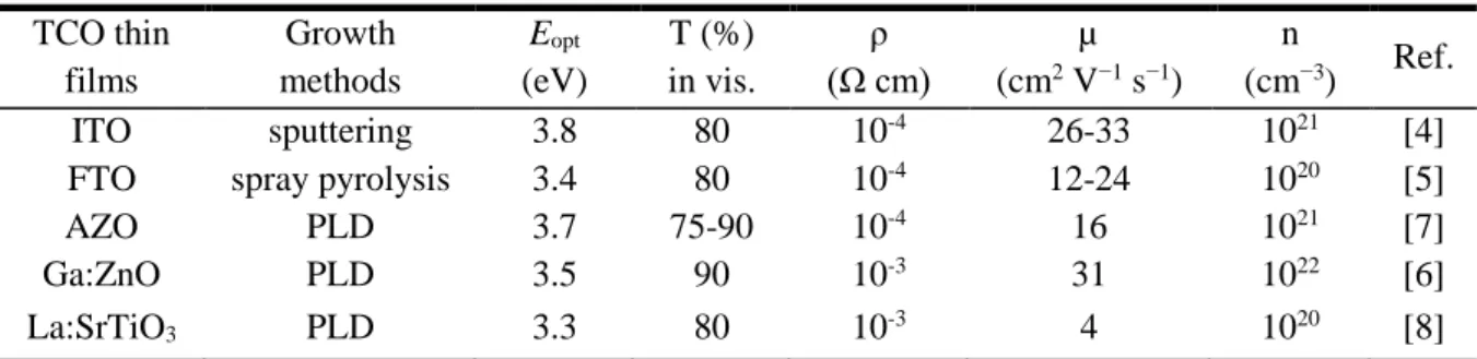
Transparent conductive oxides (TCOs) are multifunctional materials which simultaneously exhibit two contrasting properties, namely high metallic conductivity due to massive structural nonstoichiometry and nearly complete and insulator-like transparency in the visible range [1]. The unique properties of TCOs make them useful in many important technological applications such as flat-panel display, electrochromic window, optical communication, light-emitting diodes (LED), and photovoltaic (PV) devices, as shown in Figure 1 [2]. The first TCO was a thin film of CdO prepared by thermally oxidizing a vacuum sputtered film of cadmium metal in 1907 [3]. While CdO is not widely used because of toxicity, it remains of theoretical interest because of its high electron mobility due to a low effective electron mass. The most important TCO used in practice is tin doped indium oxide (In2O3:Sn), also called indium-tin-oxide (ITO). ITO is used as a transparent electrode in all flat panel displays, due to its high optical transmission (>80% in visible range), electrical conductivity (~104 S cm-1) and large optical band gap (Eg≈3.8 eV) [4].
To date, most of the commercial TCOs are n-type, which have larger electron concentrations than hole concentrations, such as ITO, Aluminium-doped ZnO (AZO), Fluoride-doped SnO2 (FTO), etc. Table 1 summarizes the typical n-type oxides thin films in the literatures [4-8]. However, in contrast to n-type TCOs, there are only a limited number of materials which show p-type conductivity and transparency at the same time. The scarcity of
18
p-type TCOs which have larger hole concentrations than electron concentrations is due to the
strong localization on the upper edge of the valence band to oxide ions in electronic structure of oxides. Many works have been made to solve this problem by engineering electronic structures based on hybridization of O 2p orbitals with closed-shell Cu 3d10 orbitals. Recently, the Cu-based oxides have been investigated, such as delafossite materials CuAlO2 [9]. Table 2 summarizes the p-type oxides thin films in the recent literatures [9-13].
Figure 1. Various applications of transparent conducting oxides (TCOs). Adapted from [2].
Table 1. A brief summary n-type TCOs thin films in the literatures. TCO thin films Growth methods Eopt (eV) T (%) in vis. ρ (Ω cm) µ (cm2 V−1 s−1) n (cm−3) Ref. ITO sputtering 3.8 80 10-4 26-33 1021 [4]
FTO spray pyrolysis 3.4 80 10-4 12-24 1020 [5]
AZO PLD 3.7 75-90 10-4 16 1021 [7]
Ga:ZnO PLD 3.5 90 10-3 31 1022 [6]
La:SrTiO3 PLD 3.3 80 10-3 4 1020 [8]
PLD: pulsed laser deposition; Eopt: optical band gap; T: optical transmittance; ρ: electrical resistivity; µ: carrier mobility; n: carrier concentration.
19
Table 2. A brief summary p-type TCOs thin films in the literatures. TCO thin films Growth methods Eopt (eV) T (%) ρ (Ω cm) µ (cm2 V−1 s−1) n (cm−3) Ref. CuAlO2 PLD 3.5 70 3 0.1 1019 [9] CuGaO2 PLD 3.6 80 50 0.2 1018 [12] NiO PLD 3.7 95 118 − − [13] Li:NiO sputtering 3.4 30 0.14 − − [11] MoO3 PLD 3.3 72 0.02 − − [10]
1.1.2. Epitaxial thin film
Thin film is coated onto a “substrate” surface to form layer whose material in thickness ranging from nanometers (nm) to micrometers (µm). The thin film deposition techniques including the physical and chemical deposition methods, are widely used in solar panels, disk drives, and optical devices [14]. Chemical deposition, i.e., chemical vapor deposition (CVD), is used to fabricate the high purity solid materials in a form of film, when a volatile fluid precursor produces a chemical change on a surface leaving a chemically deposited coating. Physical Deposition, i.e., physical vapor deposition (PVD) including thermal evaporation and sputtering,
is the most common and useful physical technology where a material is released from a source and deposited on a substrate using electromechanical or thermodynamic processes [15]. Epitaxy is in regard to the growth of a crystalline thin film on the surface of a crystalline substrate whose crystal orientation imposes a crystalline order onto the thin film. Thus, the film can be grown up to a certain thickness (e.g., nanometers) in crystal structures differing from their bulks. The epitaxial growth of thin films is generally achieved by the film deposition techniques, including molecular beam epitaxy (MBE), CVD and pulsed laser deposition (PLD),
20
resulting in the lower density of defects in the films and the fabrication of films with different doping levels [16].
Moreover, understanding of the different mechanisms affecting the growth mode is necessary to control the surface morphology during thin film growth. Two independent processes: nucleation and growth of islands play an important role during vapor-phase epitaxial growth on an atomically flat surface. The thermodynamic approach to crystal growth is used to describe crystal growth close to equilibrium, that is, for a thermodynamically stable system. This thermodynamic approach has been used to determine growth modes of thin films close to equilibrium [17], that is, only at small or moderate supersaturation. Three different growth modes, schematically depicted in Figures 2(a) (b) (c) can be distinguished [18].
1) Island growth (Volmer-Weber) • form three dimensional islands;
• film atoms more strongly bound to each other than to substrate; • and/or slow diffusion.
2) Layer by layer growth (Frank -van der Merwe) • generally highest crystalline quality;
• film atoms more strongly bound to substrate than to each other; • and/or fast diffusion.
3) Mixed growth (Stranski-Krastanov)
21
Figure 2. Three different growth mode: (a) Island growth; (b) Layer by layer growth; (c) Mixed growth.[18]
1.1.3. Perovskite oxides
Perovskite is a type of crystal structure in the family of transition metal (TM) oxides, in addition to the spinel, scheelite and pyrochlore. Perovskite oxides show the remarkably versatile chemical and physical properties due to the unique nature of TM’s outer d orbital electrons. This gives cations with several oxidation states and the metal-oxygen bonding varying from nearly ionic to metallic. Perovskite oxides are used in electronics and telecommunication because of their prominent superconductivity, magnetoresistance, dielectric properties and ferroelectricity [19]. There are many different types of distortions in perovskites, including the tilting of the octahedra, distortions of the octahedra driven by electronic factors (i.e., Jahn-Teller distortions [20]), etc. This could reduce the symmetry of crystal structure, thus influences some physical properties such as the electronic, magnetic and dielectric properties.
Schematic diagram of the typical perovskites structure is shown in Figure 3 [21]. The structure of perovskite is a primitive cubic structure of the general stoichiometry ABO3 (space group Pm3-m), containing two kinds of cations and one kind of oxygen anion. One of the cation
22
sublattices is built-up by “A” cations with a coordination number of 12, surrounded by 8 corner-sharing BO6 octahedra.
Figure 3. Schematic illustration of ideal perovskite structure ABO3 [21].
The tailoring of the physical properties for perovskites from their parent compounds by substitutions could be achieved by the distortion of structures due to the A and/or B non-isovalent substitutions. Taking the typical cubic perovskite BiFeO3 as example [22], the divalent (+2), trivalent (+3) or tetravalent (+4) cations (e.g., Sr, Cr, Pb, respectively) substitution or doping for A and B-sublattice have been extensively studied to optimize its FE and ferromagnetic properties [23]. The cations may be either randomly distributed or adopt an ordered configuration as the multiple cations substitution into either the A or B-sites, where the ordering of the cations strongly depends on the differences of their charges and sizes.
Double perovskites evolved from their primitive unit of perovskite ABO3 (or A2B2O6) can be represented by the general formula AA'B2O6 (1:1 A-site ordering) and A2BB'O6 (1:1 B-site ordering), exampling CaFeTi2O6 (Figure 4(a)) [24] and La2NiMnO6 (Figure 4(b)) [25], La2BMnO6 [26], La2FeMnO6 [27], Bi2FeCrO6 [28], respectively. Additionally, the AA'BB'O6 also represents the double perovskite structure with both A- and B-site ordering, such as NaLaMgWO6 (Figure 4(c)) [29].
23
Figure 4. Crystal structure of (a) A-site ordered double perovskite CaFeTi2O6; (b) B-site ordered double perovskite La2NiMnO6 and (c) both A- and B-site ordered double perovskite NaLaMgWO6.[24, 25, 29]
Among these types of double perovskites, the modified A2BB'O6 structure (see Figure 5) with B-site aliovalent substitutions and the BO6 and B′O6 octahedra which are alternatively arranged in two interleaving face-center-cubic (FCC) sublattices [30]. The A sites are usually occupied by alkaline ions, while the B sites correspond to TM ions. Double perovskites
A2BB'O6 materials are the promising candidates for electronic devices owing to their physical characteristics (e.g., magnetic properties) resulting from the strong super-exchange couplings between various combinations of 3d, 4d and 5d elements [31].
Figure 5. Representative crystal structure of double perovskite A2BB'O6 showing BO6 and B′O6 octahedra.[30]
24 1.1.4. Ferroelectricity
In dielectric materials, the presence of an external electric field (Eext) induces an internal electric field (Eint) due to the free charges, electric dipoles or atomic polarizability which tend to screen the applied Eext. Under certain conditions, electric dipoles of the material can be aligned in the same direction and give rise to a spontaneous polarization. This phenomenon discovered in 1920 is called ferroelectricity [32]. FE materials are characterized by a transition temperature, the Curie temperature TC between paraelectric and FE phases. Ferroelectrics are a class of materials with a permanent polar axis, and the polarization direction can be switched by applying an Eext. At temperatures above TC, the crystals are non-polar and no longer FE and behave like normal dielectrics, as known as paraelectrics. One of the best known examples is BaTiO3 (Figure 6) [33]. They are widely used for designing sensors, tunable capacitors, as well as FE random access memories in which the information is stored by the remnant polarization [34].
Figure 6. Atomic structures of perovskite BaTiO3 in (a) the paraelectric cubic phase at high temperature and FE phase with upward (b) and downward (c) polarization at RT.[33]
25
In ABO3 perovskites, a central positive B-ion is surrounded by an octahedron of oxygen ions with negative charges (O2-), whose position shifting during structural phase transitions (e.g., cubic to tetragonal) would break the inversion symmetry and induces the dipole moment, thus demonstrating the FE order. For example, the BaTiO3 with paraelectric cubic phase at high temperature transfers to BaTiO3 with FE phase at RT (Figure 6) [34]. In the most of FE perovskites, the B-site atom has an empty d electron shell allowing covalent bonding with the full p orbitals of the O atoms. Ferroelectricity can also occur due to the existence of lone pairs of electrons on the outer shell of the A-site atom, which are highly susceptible to polarization [35].
Figure 7. Polarization (P) − Electric field (E) characteristics for different polarization types: I: Dielectric polarization; II: Paraelectric polarization; III: FE polarization. Inspired from [36].
Some materials are polarized by an Eext and show a linear relationship between polarization and electric field (P-E), as known as dielectric polarization (Figure 7, I). Some paraelectric materials demonstrate a more pronounced nonlinear polarization (Figure 7, II) [36]. The electric permittivity is a function of the Eext, corresponding to the slope of the polarization curve. Additionally, FE materials show a spontaneous (zero field) polarization
26
(Figure 7, III). The direction of the spontaneous polarization can be reversed by an applied
Eext, and demonstrating a hysteresis loop. 1.1.5. Magnetism
The filling of the atomic orbitals with electrons is given by Hund’s rules [37], and results from the competition between the Pauli Exclusion principle [38] and the Coulomb repulsion [39]. As the Pauli Exclusion prevents two spins to occupy the same quantum state simultaneously, two parallel spins have to occupy in different orbitals whereas two anti-parallel spins can occupy in the same orbital. Therefore two parallel spins save some Coulomb energy compared to two anti-parallel spins. A mechanism able to induce magnetic moments on atoms with partially filled external orbitals. The exchange interaction between magnetic species in a solid [40] leads to a magnetic order which depends of the system symmetry: (1) For positive exchange interaction, magnetic ordering leads to a net magnetic moment at zero field, called ferromagnetism. (2) For negative exchange interaction, magnetic ordering leads to a zero net magnetic moment, called antiferromagnetism. These energy terms are in competition with thermal agitation and above a TC for ferromagnetism and Néel temperature (TN) for antiferromagnetism, the magnetic order disappears in a paramagnetic phase [41].
The magnetic material displays the attractive or repulsive forces with another piece of the same material, which is widely used for recording and storing data devices [42]. Magnetic properties owing to the presence of unpaired electrons are mainly exhibited by materials containing TMs, which induced by their partially filled d orbitals. When the magnetic moments are oriented randomly, it is called a paramagnet, and the moments can be aligned by the applied external magnetic field (Mext).
27
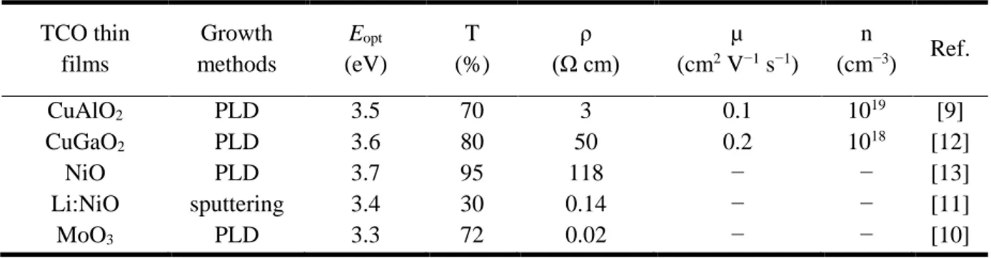
The main types of magnetic behaviors including paramagnetic, ferromagnetic and antiferromagntic are schematically illustrated in Figure 8 (a)-(e).
Figure 8. Schematic illustrations of spin interactions for several 2-D magnetic behaviors in 3-D magnetic phenomena: (a) 2-3-D paramagnetic disordered spins, (b) 2-3-D ferromagnetic ordered spins, (c) D antiferromagnetic ordered spins, (d) D ferrimagnetic ordered spins, and (e) 2-D weak ferromagnetic ordered spins. (f) Variation of M(H) for corresponding types of magnetic interactions.[43]
Figure 8(a) shows a paramagnetic behavior in ferromagnetic materials without any spins interaction. The spin coupling enables to demonstrate the parallel or antiparallel interactions for ferromagnetic or antiferromagnetic coupling, respectively (Figure 8(b)(c)). Ferrimagnet with an inverse spinel structure is caused by the antiferromagnetic coupling, and a net magnetic moment is induced, as shown in Figure 8(d). Figure 8(e) shows the magnetic ordering termed weak ferromagnet or equivalently canted antiferromagnet, which produced by the incomplete cancellation of magnetic moments in the systems where all spins are equivalent. The ferro-, antiferro-, ferrimagnetic, and weak ferromagnetic ordering occur below a critical
28
or magnetic ordering temperature, TC. Figure 8(f) shows the magnetization−magnetic field (M(H)) variations for the corresponding types of magnetic interactions [43]. The magnetization, M (= χH), where H is the applied magnetic field and χ is susceptibility. M(H) increases with increasing H prior to reaching a maximum value (the saturation magnetization). Ferro- or ferrimagnets exhibit a spontaneous magnetization, although with different saturation magnetization values.
1.1.6. Multiferroic materials
In 19th century, Maxwell equations first combined the electronic and magnetic properties. The electric and magnetic ordering in solids are most often considered separately due to the charge effects of electrons and ions, whereas electron spins govern magnetic properties. For example, in spintronics [44], the effects of spins on the transport properties of solids allow the possibility to control one by the other.
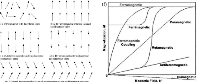
In the recent few decades, multiferroic materials showing more than one type of ferroic order in one phase simultaneously (e.g., ferromagnetism, ferroelectricity or ferroelasticity) have been extensively studied for understanding the interaction between magnetic and electric coupling, and potential multifunctional applications [45-47]. Morever, the coupling between magnetic and electric properties, called magnetoelectric effect, induces the possibility of tuning electrical polarization and magnetization by applying an Mext and Eext, respectively [48, 49], as shown in Figure 9.
29
Figure 9. Summary of all the functionalities of multiferroic materials. E and P represent electric field and polarization, H and M represent magnetic field and magnetization, and σ and ε are stress and deformation, respectively.[30]
Generally, most of studied typical multiferroics are perovskite TM oxides like TbMnO3, HoMn2O5 and bismuth compounds like BiFeO3, BiMnO3, as shown in Figure 10. The single-phase multiferroics comprise two types according the originality of ferroelectricity, including Type I: proper multiferroics and Type II: improper multiferroics.
Type I multiferroics have been known for a long time, which are good ferroelectrics and antiferromagnetic with high FE and lower magnetic ordering temperatures. The most typical materials are BiFeO3 (TC = 1100 K, TN = 643 K) [50], YMnO3 (TC = 914 K, TN = 76 K) [51], BiMnO3 and PbVO3 (Figure 10). The magnetoelectric coupling between the FE and magnetic ordering is usually weak due to the each other’s independent properties.
Type II multiferroics include rare-earth manganites such as TbMnO3, HoMn2O5 (Figure 10) with low ferroelectricity and ordering temperatures (e.g., 28 K for TbMnO3 [52]), low net magnetization due to antiferromagnetic spin-spiral structures and low polarization in
30
the order of 10−2 μC cm-2 [53]. Other, non-perovskite multiferroic oxides, such as LuFe
2O4 and
LiCu2O2 and non-oxide multiferroics such as BaNiF4 and ZnCr2Se4.
Figure 10. Classification of insulating oxides including FE, ferromagnetic and multiferroic materials and corresponding representative materials. [54]
1.2. Multiferroic Bi2FeCrO6 1.2.1. Synthesis method
Bi2FeCrO6 (BFCO) is expected to take in a simple perovskite structure with random occupancy of Fe3+ and Cr3+ on the B site, since the long range B-site ordered double-perovskite compound is not likely to form due to the same valence state and near ionic radii (rFe3+ = 0.645 Å and rCr3+ = 0.615 Å) of Fe3+ and Cr3+. Whereas some experimental results demonstrated that the ceramic Bi(Fe,Cr)O3 epitaxial thin films are isostructural to rhombohedral double-perovskite BiFeO3,
31
showing a large FE polarization of ~55 μC cm-2 and a small magnetization at RT due to the lack of Fe/Cr cation ordering along the (111) cubic direction in the samples. Nechache et al.[55] firstly reported the growth of epitaxial BFCO multiferroic thin films on adequate substrates under controlled conditions using a physical synthesis method, that is pulsed laser deposition (PLD), and characterizations of the remarkable FE and ferrimagnetic properties.
Figure 11. Pressure of oxygen (PO2) − temperature of substrate (Ts) phase diagram for thin films of the Bi–Fe–Cr–O system grown by PLD.[56]
Pulsed Laser Deposition (PLD) is one of the most useful and simple synthesis method to grow complex oxides, like LaBiFeCrO6 [57], BFCO, La2FeCrO6 [58] under controlled optimal conditions including laser fluence, substrate temperature, oxygen/gas partial pressure, etc. Thus, multiferroic BFCO thin film is fabricated by PLD techniques, generally grown on the crystalline substrates like SrTiO3 (STO), LaAlO3, (LaAlO3)0.3(Sr2AlTaO6)0.7 (LSAT), MgO and metal-oxides coated Si wafer (e.g., Nb-STO/MgO/Si wafer [59]). Nechache et al.[55] reported that a single crystal (001)-oriented BFCO phase is obtained at a substrate temperature (TS) of 680 °C and oxygen pressure (PO2) of 8 mTorr. The deviation from this oxygen pressure
32
during the BFCO growth results in the appearance of secondary phases, such as the Bi2O3 (BO) at relatively high TS and PO2; and (FeCr)3O4 (FCO) at lower TS and PO2. This dependence on
TS and PO2 is due to the presence of highly volatile bismuth in the film which is sensitive to the deposition parameters. Several elements point toward a relationship between nonstoichiometry (i.e., oxygen vacancies and cation deficiency) and the destabilization of the BFCO single phase. The various phase formation under different growth conditions is graphically summarized in the phase diagram presented in Figure 11.
1.2.2. Crystal structure and cationic ordering
The lowest energy and stable structure of double perovskite BFCO has R3 symmetry (space group # 146, rhombohedral) which is different from the cubic double perovskite due to the alternating rotations of oxygen octahedra around Fe/Cr cations. The magnetic order becomes ferrimagnetic while every Cr spin orienting upward and Fe spin downward. The experimental lattice constant a = 5.537 Å and c = 13.502 Å (α = 60.20°) are intermediate values of existing experimental results [55, 60-62]. After internal structure optimization, every atom has a displacement from that of the cubic perovskite structure.
Table 3. Optimized internal structural parameters of BFCO with the Rc crystal structure [28].
Atom Parameter Values
Bi Z1 0.0005, 0.5040 Fe/Cr Z2 0.7330 / 0.2260 O x 0.5433, 0.0511 y 0.9542, 0.9043 z 0.3937, 0.4459
33
Figure 12. Crystal structure of double perovskite Bi2FeCrO6. The left-side is used to describe the relative positions of the atoms, and the right-side is the primitive cell.[28]
The crystal structure and primitive cell are illustrated in Figure 12. The optimized parameters are summarized in Table 3. The bond lengths and Fe-O-Cr bond angle can be calculated from the structural parameters. The calculated values are summarized in Table 4.
Table 4. Bond lengths (Å) and Fe-O-Cr angle (°) of BFCO with the Rc crystal structure [28].
Furthermore, Nechache et al.[56] pointed out that the Fe/Cr cation ordering in epitaxial BFCO single phase plays a crucial role in establishing the good FE and ferromagnetic properties. They have demonstrated the presence of the Fe/Cr cation ordering and quantified it in the BFCO single phase through some experimental approaches. The alternation of octahedral FeO6 and CrO6 is achieved only in the (111) cubic direction of BFCO phase from different types of stacking in Figure 13(a). The superstructure reflections (00l), where l is 1, 2, 3, are
Bond length Fe-O 2.130, 1.971
Cr-O 1.947, 1.994
Bi-O 2.347, 2.387
2.406, 2.416
34
visible in the (001)-oriented BFCO thin films grown on single-crystal (100)-oriented STO substrates by PLD, not shown here. The reciprocal space mapping (RSM) of X-ray diffraction (XRD) around the (111) cubic reflection of STO was performed to determine the Fe/Cr cationic ordering. The RSM diagram in Figure 13(b) reveals the existence of two extra spots (1/2 1/2 1/2 and 3/2 3/2 3/2) in addition to the (111) main reflection of STO and BFCO. The periodicity of the superstructure reflections is about 4.58 Å, which is double the (111) perovskite cubic distance BFCO d½½ ½ /2 ≈ STO d111 (2.28 Å).
Figure 13. (a) Different types of Fe and Cr octahedral stacking in BFCO along (001) and (111) cubic directions; (b) RSM scan around (111) reflection for (001)-oriented BFCO films. (c) Sketch of the double-perovskite crystal structure and corresponding pseudo-cubic unit cell of BFCO, showing (111) direction.[63]
This doubling of the perovskite unit cell suggest the existence of the Fe/Cr ordering in the films along the (111) crystal structure (Figure 13(c)). A detailed analysis of the normalized intensity of the superstructure peaks was carried out to quantify the degree of Fe/Cr cationic
35
ordering, which was estimated from the normalized ratio of the superlattice peak intensity to the main (111) reflection intensity of BFCO. Thus, degree of cationic ordering, R = I222/I111 × 100%.
1.2.3. Optical properties
Optical properties of BFCO relative to the optical dielectric function, optical conductivity and optical absorption are expected to further study in theoretical and experimental research. Song
et al.[28] reported a study on electronic and optical properties of BFCO from first principle
investigation using the combination of a full-potential density-functional-theory (DFT) method with Monte Carlo simulation. They calculated the direct electronic contributions of the optical dielectric function ε(ω) and optical conductivity σ(ω) curves of the BFCO as functions of photon energy (ω). Considering that the semiconductor gaps have important impact on the low-energy parts of these optical functions, they calculated them with both Generalized Gradient Approximation (GGA) and modified Becke-Johnson exchange potential (mBJ). These results, both real (Re) and imaginary parts (Im) between 0 and 12 (or 13) eV, are presented in Figure 14.
36
Figure 14. Optical dielectric functions (a) and electric conductivity (b) as functions of photon energy, both real (solid) and imaginary (dotted) parts of double-perovskite BFCO.[28]
For Re(ε), the GGA result of the low energy limit is higher than the mBJ one, having the similar trend at the energy ≥1.5 eV. For Im(ε), the main difference appears at low energy (<1.5 eV). There is a sharp peak at 0.75 eV for the GGA result, which is related to the steep decrease in the GGA curve of Re(ε) at the same photon energy. The mBJ result of Im(ε) is equivalent to zero in this region, which indicates the broad semiconductor gap from mBJ. For the σ(ω) curves, the main difference also appears at the low energy region. Re(σ(ω)) has a peak at 1.0 eV and Im(σ(ω)) has a valley at 0.5 eV. For the higher energy, both of the σ(ω) curves have similar behaviors [28]. These calculated optical functions could be useful in exploring the optical properties of double-perovskite BFCO and others similar materials.
Figure 15. UV-visible absorption coefficient of 100 nm-thick BFCO films grown on STO substrates by PLD with various cationic ordering R and compared with BiCrO3 (BCO) and BiFeO3 (BFO) thin films.[64]
37
Additionally, the optical absorption coefficient is also a crucial important parameter for the double-perovskite multiferroic BFCO as a functional layer in solar energy conversion application. Nechache et al.[64] devoted to experimentally study the effect of Fe/Cr cationic ordering (the ratio of degree of Fe/Cr cationic ordering: R) in BFCO single phase on optical absorption properties. Figure 15 shows that the higher value of R, the higher absorption coefficient α (up to ~2.3×105 cm-1). Morever, the values of α for BFCO with various R are much more significant than both BiCrO3 (absence of Fe3+) and BiFeO3 (absence of Cr3+) thin films at visible range due to the modification of TM–oxygen bond lengths and their interaction energies including the hybridization energy and Coulomb repulsion caused by the absence of either Fe3+ or Cr3+ in perovskite structure (typical perovskite formula: ABO3) [65].
1.2.4. Multiferroic properties
The B-site ordered double-perovskites oxides with general formula A2BB'O6 are two different 3d TM ions (B and B') inducing an intrinsic strong ferromagnetic interaction. According to the Kanamori-Goodenough rules [66, 67], ferromagnetism appears when one TM ion with eg electrons (B) and another without eg electrons (B') are ordered (B-O-B') at the B-sites of the perovskite structure. In the ferroelectricity-magnetism coexisted single phase, the atoms move off the center to induce electric dipole moment (i.e., FE polarization), different from the magnetic moment (i.e., magnetization).
Recently, the multiferroic and B-site ordered (B-O-B') double-perovskite BFCO has been extensively investigated. In the predicted BFCO material by first-principles calculations [28], the ferroelectricity is due to the 6s2 lone pair on Bi3+ ions, a well-established mechanism in other multiferroics, such as BiMnO3 [68] and BiFeO3 [69], while magnetism is introduced via
38
ferrimagnetic behaviour. The coupling between neighboring Cr and Fe magnetic moments is robustly antiferromagnetic and the difference between their magnetizations yields a net magnetization for BFCO. According to the works, the hypothetical double perovskites BFCO, where Fe3+/Cr3+ should be long-range-ordered (Figure 16), would have a magnetic moment of ~2 μB per formula unit (~160 emu cm-3) at 110 K [70] resulting from the antiferromagnetic exchange interaction between 5d Fe3+ and 3d Cr3+ in opposite directions and a FE polarization of ~80 μC cm-2.
Figure 16. Long range B-site ordered double-perovskite structure of Bi2FeCrO6 with the arrangements of octahedral FeO6 and CrO6. Adapted from [63].
Nechache et al.[63] reported that B-site ordered double-perovskite BFCO single phase showed a large magnetization and FE polarization. Magnetic properties of BFCO thin films are shown in Figure 17(a) demonstrating a saturated magnetic moment of ~2×10⁻⁴ emu (electromagnetic units) measured at applied magnetic field of 5 kOe, at both 300 and 10K [56]. Additionally, the measurements of M(H) curves using SQUID magnetometer with an applied magnetic field of 10 kOe at both 300 and 10K were carried out and showed the saturation magnetization of ~145 emu per cubic centimeters (emu/cc), which corresponds to ~0.96 Bohr
39
magneton (μB) per cation site or ~1.91μB per Fe–Cr pair (i.e., ~1.91μB per BFCO formula unit) [56].
Figure 17. (a) M(H) curves measurement of mutilferroic BFCO at 300 and 10 K temperature. (b) Current vs. applied voltage curve and the corresponding FE hysteresis loop obtained at RT for a 200 nm-thick BFCO film. The solid line corresponds to the polarization hysteresis loop after subtracting the leakage contribution. PFM images of multiferroic BFCO thin films: (c) as-grown and (d) after switching FE domains. (e) Corresponding FE hysteresis loops at nanoscale.[56, 71]
The polarization effect could also govern the ferromagnetic super-exchange interaction. The large anisotropic overlap of the Bi 6s2 lone pair electrons and the surrounding hybridized Fe 3d-O 2p orbitals induced built-in electric field can facilitate their coupling to the long-range spin order by minimizing the magneto-elastic energy [56]. Thus, this could not only allow the direct coupling between the magnetization and polarization but also strongly enhance the
40
ferromagnetic super-exchange interactions, leading to a magnetic TC close to the FE transition. Recent infrared and magnetic characterization of 200 nm-thick BFCO film seems to confirm this fact [56]. FE properties of 200 nm-thick films deposited under optimum conditions are shown in Figure 17(b). BFCO films show FE property with a remnant polarization of 55–60 μC cm-2 along the (001) direction (after subtracting the leakage current contribution). To further understand the FE properties of BFCO at nanoscale, Figure 17(d) demonstrate the FE polarization imprint was switched during scanning, by applying either negative or positive voltages between the conducting tip and the electrode or conducting substrate, compared with the as-grown BFCO as shown in Figure 17(c). Further analysis of the FE character of BFCO films was performed by local remnant piezoelectric hysteresis loops,as shown in Figure 17(e).
1.3. Multiferroic materials for solar energy conversion applications
Effective use of renewable energy: solar, geothermal, hydroelectric, wind and biomass, is important for reducing greenhouse gas (e.g., CO2) emissions that does not lean upon fossil resources (e.g., coal, petroleum, natural gas, shell gas) [72]. Among them, solar energy is the most abundant, but limited by the utilization technologies. Although the harvesting and storage techniques of solar energy are attractive and promising to solve the environmental pollution problems, the implementation of solar energy technologies has been limited by high costs, relatively low efficiency and resource intermittency issues (Figure 18). Therefore, tremendous researches have been devoted to conversion and storage of solar energy, with a focus on increasing conversion efficiency and reducing manufacturing costs.
![Figure 4. Crystal structure of (a) A-site ordered double perovskite CaFeTi 2 O 6 ; (b) B-site ordered double perovskite La 2 NiMnO 6 and (c) both A- and B-site ordered double perovskite NaLaMgWO 6 .[24, 25, 29]](https://thumb-eu.123doks.com/thumbv2/123doknet/5005715.124830/29.892.117.780.109.290/figure-crystal-structure-perovskite-perovskite-ordered-perovskite-nalamgwo.webp)
![Figure 6. Atomic structures of perovskite BaTiO 3 in (a) the paraelectric cubic phase at high temperature and FE phase with upward (b) and downward (c) polarization at RT.[33]](https://thumb-eu.123doks.com/thumbv2/123doknet/5005715.124830/30.892.169.723.774.961/figure-atomic-structures-perovskite-paraelectric-temperature-downward-polarization.webp)
![Table 3. Optimized internal structural parameters of BFCO with the Rc crystal structure [28]](https://thumb-eu.123doks.com/thumbv2/123doknet/5005715.124830/38.892.110.774.949.1083/table-optimized-internal-structural-parameters-bfco-crystal-structure.webp)
![Figure 18. Efficiency−cost comparison of various solar energy conversion technologies.[72]](https://thumb-eu.123doks.com/thumbv2/123doknet/5005715.124830/47.892.212.672.114.426/figure-efficiency-comparison-various-solar-energy-conversion-technologies.webp)
![Figure 27. Principle of hydrogen production by water electrolysis using a semiconductor photoelectrode.[97]](https://thumb-eu.123doks.com/thumbv2/123doknet/5005715.124830/56.892.170.725.253.474/figure-principle-hydrogen-production-water-electrolysis-semiconductor-photoelectrode.webp)

