HAL Id: inria-00449834
https://hal.inria.fr/inria-00449834
Submitted on 22 Jan 2010
HAL is a multi-disciplinary open access
archive for the deposit and dissemination of
sci-entific research documents, whether they are
pub-lished or not. The documents may come from
teaching and research institutions in France or
abroad, or from public or private research centers.
L’archive ouverte pluridisciplinaire HAL, est
destinée au dépôt et à la diffusion de documents
scientifiques de niveau recherche, publiés ou non,
émanant des établissements d’enseignement et de
recherche français ou étrangers, des laboratoires
publics ou privés.
A Parallel and Modular Architecture for 802.16e LDPC
Codes
François Charot, Christophe Wolinski, Nicolas Fau, François Hamon
To cite this version:
François Charot, Christophe Wolinski, Nicolas Fau, François Hamon. A Parallel and Modular
Archi-tecture for 802.16e LDPC Codes. 11th EUROMICRO Conference on Digital System Design
Architec-tures, Methods and Tools (DSD 2008), Sep 2008, Parme, Italy. pp.418 - 421. �inria-00449834�
A Parallel and Modular Architecture for 802.16e LDPC Codes
Franc¸ois Charot, Christophe Wolinski
Irisa, Inria
University of Rennes 1
Campus de Beaulieu
35042 Rennes Cedex, France
{charot,wolinski}@irisa.fr
Nicolas Fau, Franc¸ois Hamon
R-Interface
Marseille Innovation BP 20038
Pˆole M´edia Belle de Mai
13302 Marseille Cedex 03
{fau,hamon}@r-interface.com
Abstract
We propose a parallel and modular architecture well suited to 802.16e WiMax LDPC code decoding. The pro-posed design is fully compliant with all the code classes de-fined by the WiMax standard. It has been validated through an implementation on a Xilinx Virtex5 FPGA component. A four or six-module FPGA design yields a throughput rang-ing from 10 to 30 Mbit/s by means of 20 iterations at a clock frequency of 160 MHz which mostly satisfies communica-tion throughput in the case of the WiMax Mobile communi-cation.
1 Introduction
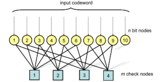
Low density parity-check (LDPC) are linear block codes. They have recently been included as error correcting codes in several new communication standards. A codeword of an (n, k) LDPC code must satisfy m = n − k parity check equations on its n codeword bits. The whole set of (n − k)equations can be depicted by means of a bipartite graph (see figure 1), composed of two kinds of nodes: bit nodes (BN), representing the bits of the codeword and check nodes (CN), representing the parity check equations. It can also be represented by a sparse parity check matrix H of size m-by-n, where n is the length of the code and m is the number of parity-check bits in the code, specifying the parity-check constraints of the bits in the codewords.
The hardware realization of an LDPC decoder is deter-mined by many strongly interrelated parameters, leading to a large design space and various implementations [1, 4, 7, 3]. For a fully parallel hardware realization, each node is instantiated and the connections between them are hard-wired. Even for relatively short block length, severe routing congestion problems occur. Therefore partly parallel archi-tectures (where the nodes of only one subset at a time are
sources) requires an architectural exploration phase based on methodologies and tools to solve complex optimization problems. 1 2 3 4 5 6 7 8 9 10 n bit nodes 1 input codeword m check nodes 2 3 4
Figure 1. Bipartite graph of a LDPC code. The parallel and modular architecture well suited to LDPC code decoding presented in this paper is made up of several processing modules communicating through an optimized interconnection structure. Each processing mod-ule includes two processing units (called bit node and check node), and a set of memory banks. The size of the architec-ture – number of modules, number of interconnection buses, size and number of memory banks – is both communication standard and throughput dependent. The size of the archi-tecture in the case of a given standard and a given through-put can be established during the space exploration process thanks to our optimization system based on a constraints programming approach.
The paper is structured as follows. Our decoding LDPC algorithm and its performance are summarized in section 2. Our architecture is outlined in section 3. Implementation results of a WiMax LDPC decoder are presented in section 4. Finally some conclusions are given in section 5.
2 LDPC Code Decoding algorithm
The LDPC decoder achieves good performance with the
model is:
rn= sn+ vn
where rnis the received noisy symbol, sn= +/-1, the
trans-mitted BPSK symbol and vnis an additive white Gaussian
noise with variance σ2 = N
O/2. The log-likelihood ratio
of bit n is:
un= (2/σ2).rn
The BP-based algorithm operates as follows. Let vn→m
denote the message sent from by the bit node n to the check
node m and let wm→n denote the message sent from the
check node m to the bit node n.
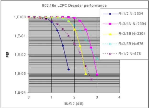
Figure 2. 802.16e LDPC decoder perfor-mance.
The check node update for each iteration of the algorithm is defined by:
wm→ni= g(vn0→m, vn1→m, ..., vndc−1→m)
where dc is the degree of the check node, it is to say the number of bit nodes connected to the considered check node.
G(x, y) = sign(x).sign(y)Min(| x |, | y |)
+ ln(1 + e−|x+y|) − ln(1 + e−|x−y|)
In [2] the following simplification is proposed:
g(x, y) = sign(x).sign(y)M in(| x |, | y |)/α (1)
Where α is a normalization factor greater than one. The bit node update for each iteration of the algorithm is defined by:
vn→mi= un+
!
mj∈M(n)
wmj→n− wmi→n (2)
The iterations are completed applying the following rule on the codeword:
hard decision "
0, if (vn→mi+ wmi→n) ≥ 0
1, if (vn→mi+ wmi→n) < 0
The figure 2 illustrates the decoder performance in terms of packet error rate (PER) when applied to the 802.16e LDPC codes. The results are given for 6-bit LLR quanti-zation and 20 decoding iterations. Two code lengths are considered: n=576 bits and n= 2384 bits with four coding rates: r=1/2, 2/3, and 3/4 and 5/6.
3 Proposed Decoding Architecture
In order to ensure at the same time flexibility and the de-manded throughput, partly parallel architectures are manda-tory. Instead of exploiting the inherent parallelism in the sub-matrices of the H parity-check matrix as in [6], we propose to have a global approach to the problem by per-forming the calculation of independent CN or BN nodes in parallel. In this section, the exploited data decomposition is first explained. We then focus on the computation distri-bution and the memory organization and show how bit node and check node computations are performed.
Our approach consists in clustering nodes of the whole set of check nodes (CN nodes) (respectively bit nodes, BN
nodes) into independent sets called CSj(respectively BSj)
according to the features of the parity check matrix H.
CSj= {CNi| 24.j ≤ i ≤ 24.(j + 1) − 1} 0 ≤ j < 11
BSj= {BNi| 24.j ≤ i ≤ 24.(j + 1) − 1} 0 ≤ j < 23
The left part of the figure 3 indicates the bit nodes
re-quired to compute two sets of check nodes: CS0 (from
CN0to CN23) and CS1(CN24to CN47). It is shown that
in order to compute CN0belonging to set CS0, a message
comes from nodes BN47, BN66, BN205, BN236, BN289
and BN312. These six bit nodes belong respectively to sets
BS1, BS2, BS8, BS9, BS12and BS13. The right part of
the figure shows that BN47belonging to set BS1also has
an edge with check node CN41belonging to set CS1.
Set BS1 is composed of bit nodes
(from 24 to 47) connected to check nodes in the Set CS1
CN24 [30, 125, 163, 170, 267, 312, 336] CN25 [31, 126, 164, 171, 268, 313, 337] CN26 [32, 127, 165, 172, 269, 314, 338] CN27 [33, 128, 166, 173, 270, 315, 339] CN28 [34, 129, 167, 174, 271, 316, 340] CN29 [35, 130, 144, 175, 272, 317, 341] CN30 [36, 131, 145, 176, 273, 318, 342] CN31 [37, 132, 146, 177, 274, 319, 343] CN32 [38, 133, 147, 178, 275, 320, 344] CN33 [39, 134, 148, 179, 276, 321, 345] CN34 [40, 135, 149, 180, 277, 322, 346] CN35 [41, 136, 150, 181, 278, 323, 347] CN36 [42, 137, 151, 182, 279, 324, 348] CN37 [43, 138, 152, 183, 280, 325, 349] CN38 [44, 139, 153, 184, 281, 326, 350] CN39 [45, 140, 154, 185, 282, 327, 351] CN40 [46, 141, 155, 186, 283, 328, 352] CN41 [47, 142, 156, 187, 284, 329, 353] CN42 [24, 143, 157, 188, 285, 330, 354] CN43 [25, 120, 158, 189, 286, 331, 355] CN44 [26, 121, 159, 190, 287, 332, 356] CN45 [27, 122, 160, 191, 264, 333, 357] CN46 [28, 123, 161, 168, 265, 334, 358] CN47 [29, 124, 162, 169, 266, 335, 359] Bit nodes CN0 BN47 BN66 BN205 BN236 BN289 BN312 Check nodes CN41 CN0 [47, 66, 205, 236, 289, 312] CN1 [24, 67, 206, 237, 290, 313] CN2 [25, 68, 207, 238, 291, 314] CN3 [26, 69, 208, 239, 292, 315] CN4 [27, 70, 209, 216, 293, 316] CN5 [28, 71, 210, 217, 294, 317] CN6 [29, 48, 211, 218, 295, 318] CN7 [30, 49, 212, 219, 296, 319] CN8 [31, 50, 213, 220, 297, 320] CN9 [32, 51, 214, 221, 298, 321] CN10 [33, 52, 215, 222, 299, 322] CN11 [34, 53, 192, 223, 300, 323] CN12 [35, 54, 193, 224, 301, 324] CN13 [36, 55, 194, 225, 302, 325] CN14 [37, 56, 195, 226, 303, 326] CN15 [38, 57, 196, 227, 304, 327] CN16 [39, 58, 197, 228, 305, 328] CN17 [40, 59, 198, 229, 306, 329] CN18 [41, 60, 199, 230, 307, 330] CN19 [42, 61, 200, 231, 308, 331] CN20 [43, 62, 201, 232, 309, 332] CN21 [44, 63, 202, 233, 310, 333] CN22 [45, 64, 203, 234, 311, 334] CN23 [46, 65, 204, 235, 288, 335] CS0 CS1
Set BS1 is composed of bit nodes
(from 24 to 47) connected to check nodes in the Set CS0
Figure 3. Dependency relations between bit nodes and check nodes.
All nodes of a given CS or BS set are processed in the same computation unit called a module. All the nodes of the set are then processed sequentially. According to the degree of parallelism of the architecture (number of mod-ules), nodes of different CS sets (respectively BS) can be processed in parallel on different modules.
The architecture is illustrated in figure 4. It is made up of several processing modules communicating through an optimized interconnection structure. Each processing module includes two processing units (called bit node and check node), and a set of memory banks. The size of the architecture– number of modules, number of interconnec-tion buses, size and number of memory banks– is both com-munication standard and throughput dependent.
Each module has its own local memory used for storing the exchanged messages between check nodes and bit nodes during the computation process (corresponding to the edges of the bipartite graph). Each local memory is composed of several memory banks allowing parallel accesses to be per-formed. The basic idea is that all components of a message can be accessed simultaneously.
Figure 4. Organization of the parallel archi-tecture.
Each module is able to process check nodes as well as bit nodes. In the case of check node processing, the data comes from their local memories. The local memories of the module contain all the messages coming from the re-lated BN sets. After the processing accomplished in the module, results are stored in the same local memories. In the case of bit node processing, the data can come from local or non-local memories according to the correspond-ing parity matrix. In the case of non-local memory, a data transfer through the interconnection structure is performed. The interconnection structure is composed of several buses (Bi). Bi allows the data reception from any
mem-ory bank MBi,kof any module Mk, or the data sending to
any MBi,k.
timized in order to speedup the application execution. This is done thanks to our optimization system based on a con-straints programming approach. The optimization system is not described in the paper. However some results obtained with the system are presented in the next section.
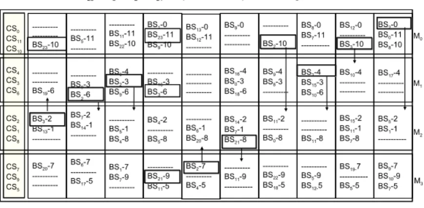
Figure 5 shows the memory organization in the case of a four-module architecture (case r = 1/2). The 12 check nodes sets that have to be calculated are distributed between the 4 modules at the rate of 3 sets per module. Six compu-tation steps (called scenarii) allow all bit node sets to be processed.
4 Case Study
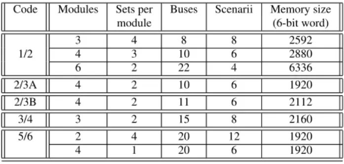
Table 1 summarizes the results of the architecture ex-ploration phase which allows different configurations of the architecture to be compared. For each code ratio of the WiMax LDPC standard, the table gives, for a given number of modules, an optimal solution in terms of CN set quantity per module, bus quantity of the interconnection structure, scenario quantity required for the computation of the BN sets and memory size required to store the messages during the decoding.
Table 1 shows that a parallel architecture composed of 4 modules connected to a 20-bus interconnection structure is able to support all the WiMax code. Each module is in charge of at most three CS sets. It includes a local memory organized into 20 banks of 3 × 96 words.
Code Modules Sets per Buses Scenarii Memory size
module (6-bit word)
3 4 8 8 2592 1/2 4 3 10 6 2880 6 2 22 4 6336 2/3A 4 2 10 6 1920 2/3B 4 2 11 6 2112 3/4 3 2 15 8 2160 5/6 2 4 20 12 1920 4 1 20 6 1920
Table 1. Optimal solutions for the different WiMAx ratios.
PM FFs Memory Slice LUT Max Frequency
18 kb block MHz
4 10 K (14%) 92 19K (27%) 192
Table 2. Implementation results of the IP on a Xilinx Virtex5 110LXT.
A synthesizable generic VHDL IP core, fully compliant with the 802.16e standard, has been developed. It covers all the modes and ratios defined in the standard. Our generic IP core allows to switch from one ratio to another on-the-fly. The core has been synthesized with Xilinx XST on a Virtex5
---BS23-10 ---BS19-6 BS3-2 BS13-1 ---BS20-7 ---BS5-11 ---BS9-3 BS2-6 BS7-2 BS14-1 ---BS6-7 ---BS17-5 ---BS11-11 BS22-10 BS6-4 BS2-3 BS9-6 ---BS5-1 BS4-8 BS1-7 BS7-9 ---BS1-0 BS23-11 BS9-10 ---BS16-3 BS3-6 BS4-2 ---BS5-8 ---BS21-9 BS11-5 BS13-0 BS12-11 ---BS6-1 BS20-8 BS2-7 ---BS4-5 BS9-0 ---BS16-4 BS0-3 BS18-6 BS14-2 BS7-1 BS21-8 ---BS11-9 - ---BS2-10 BS9-4 BS8-3 ---BS11-2 ---BS0-8 ---BS22-9 BS18-5 BS8-0 BS7-11 ---BS2-4 BS15-3 BS10-6 ---BS11-8 ---BS5-9 BS12-5 BS12-0 ---BS3-10 BS10-4 ---BS15-2 BS11-1 BS7-8 BS19-7 ---BS5-5 BS2-0 BS0-11 BS8-10 BS17-4 ---BS5-2 BS1-1 ---BS9-7 BS10-9 BS7-5 M0 M1 M2 M3
BS23, BS3, BS2, BS21 are processed in parallel using 4 modules
Bit nodes in set BS3 are processed on module M1 using messages stored in sets BS3-2 (bank MB0,2), BS3-6 (bank MB3,1) and BS3-10 (bank MB8,0)
CS0 CS11 CS10 CS4 CS3 CS6 CS2 CS1 CS8 CS7 CS9 CS5
Figure 5. Data memory organization and scenario example for bit node and check node processing.
Memory usage can be drastically reduced when switch-ing to the ASIC implementation because in the case of the FPGA implementation, the number of memories is greater than really needed. Currently 80 memories are used for message passing in this design but less than 10% of the total 18 Kbits of each memory is used. The whole design is syn-chronous and is running at 192 MHz. In order to increase the overall clock frequency, the IP core memories have a two-cycle latency.
PM ratio ratio ratio ratio ratio ratio
1/2 2/3A 2/3B 3/4A 3/4B 5/6 1 cycles/block 884 788 788 740 740 692 Throughput 2.6 3.94 3.94 4.74 4.74 5.27 4 cycle/block 236 212 212 212 212 188 Throughput 10.4 15.8 15.8 19.2 19.2 21.6 6 cycle/block 164 164 164 140 140 140 Throughput 14.84 19.78 19.78 26.34 26.34 29.26
Table 3. Performance results of the LDPC de-coder.
Table 3 gives some performance results obtained in the case of different configurations: 1, 4 and 6 processing mod-ules. The system performances are expressed by: the num-ber of cycles required for the execution of one algorithm iteration and the throughput of the IP in Mbit/sec (output payload stream rate after redundancy suppression) for 20 iterations and a 160 MHz system clock.
5 Conclusions
We have presented a parallel and modular LDPC archi-tecture. An IP core fully compliant with all the modes of the 802.16e WiMax standard has been developed and syn-thesized on a Xilinx Virtex5. A four or six-module FPGA design yields a throughput ranging from 10 to 30 Mbit/s at a clock frequency of 160 MHz. This frequency range is
compatible with the throughput requirements of the WiMax mobile standard.
Future work will consist in applying the principles of this scalable generic parallel architecture to other communica-tion standards such as the 802.11n standard. It will also include further optimizations.
References
[1] A. Blanksby and C. Howland. A 690-mW 1-Gb/s 1024-b, Rate-1/2 Low-Density Parity-Check Code Decoder. IEEE Journal of Solid-State Circuits, 37(3):404–412, March 2002. [2] J. Chen and M. P. C. Fossorier. Density Evolution for
BP-Based Decoding Algorithms of LDPC Codes and their Quan-tized Versions. In Proceedings of the IEEE Global Telecom-munications Conference, (GLOBECOM 2002), pages 1378– 1382, Nov. 2002.
[3] M. Cocco, J. Dielissen, M. Heijligers, A. Hekstra, and J. Huisken. A Scalable Architecture for LDPC Decoding. In Proceedings of the conference on Design, automation and test in Europe (DATE 2004), pages 88–93, 2004.
[4] F. Kienle, T. Brack, and N. Wehn. A Synthesizable IP Core for DVB-S2 LDPC Code Decoding. In Proceedings of the conference on Design, Automation and Test in Europe (DATE 2005), pages 100–105, 2005.
[5] D. J. C. MacKay. Good Error-Correcting Codes based on Very Sparse Matrices. IEEE Trans. Inform. Theory, 45:399–431, Mar. 1999.
[6] M. Mansour and N. Shanbhag. Architecture-Aware Low-Density Parity-Check Codes. In Proceedings of the Inter-national Symposium on Circuits and Systems (ISCAS 2003), pages 57–60, May 2003.
[7] P. Urard, L. Paumier, P. Georgelin, T. Michel, V. Lebars, E. Yeo, and B. Gupta. A 135Mbps DVB-S2 Compliant Codec based on 64800-bit LDPC and BCH Codes. In Proceedings of the Design Automation Conference, (DAC 2005), pages 547– 548, June 2005.