HAL Id: hal-01736112
https://hal.archives-ouvertes.fr/hal-01736112
Submitted on 27 Mar 2018
HAL is a multi-disciplinary open access
archive for the deposit and dissemination of
sci-entific research documents, whether they are
pub-lished or not. The documents may come from
teaching and research institutions in France or
abroad, or from public or private research centers.
L’archive ouverte pluridisciplinaire HAL, est
destinée au dépôt et à la diffusion de documents
scientifiques de niveau recherche, publiés ou non,
émanant des établissements d’enseignement et de
recherche français ou étrangers, des laboratoires
publics ou privés.
Effect of annealing environment on the memory
properties of thin oxides with embedded si nanocrystals
obtained by low-energy ion-beam synthesis
P. Normand, E. Kapetanakis, P. Dimitrakis, D. Tsoukalas, K. Beltsios,
Nikolay Cherkashin, Caroline Bonafos, Gérard Benassayag, H. Coffin, Alain
Claverie, et al.
To cite this version:
P. Normand, E. Kapetanakis, P. Dimitrakis, D. Tsoukalas, K. Beltsios, et al.. Effect of annealing
environment on the memory properties of thin oxides with embedded si nanocrystals obtained by
low-energy ion-beam synthesis. Applied Physics Letters, American Institute of Physics, 2003, 83 (1),
pp.168-170. �10.1063/1.1588378�. �hal-01736112�
Effect of annealing environment on the memory properties of thin oxides with
embedded Si nanocrystals obtained by low-energy ion-beam synthesis
P. Normand, E. Kapetanakis, P. Dimitrakis, D. Tsoukalas, K. Beltsios, N. Cherkashin, C. Bonafos, G. Benassayag, H. Coffin, A. Claverie, V. Soncini, A. Agarwal, and M. Ameen
Citation: Appl. Phys. Lett. 83, 168 (2003); doi: 10.1063/1.1588378 View online: https://doi.org/10.1063/1.1588378
View Table of Contents: http://aip.scitation.org/toc/apl/83/1 Published by the American Institute of Physics
Articles you may be interested in
A silicon nanocrystals based memory
Applied Physics Letters 68, 1377 (1996); 10.1063/1.116085 Single charge and confinement effects in nano-crystal memories Applied Physics Letters 69, 1232 (1996); 10.1063/1.117421
Silicon nanocrystal formation in annealed silicon-rich silicon oxide films prepared by plasma enhanced chemical vapor deposition
Journal of Applied Physics 101, 113510 (2007); 10.1063/1.2740335
Manipulation of two-dimensional arrays of Si nanocrystals embedded in thin layers by low energy ion implantation
Journal of Applied Physics 95, 5696 (2004); 10.1063/1.1695594
Size-controlled highly luminescent silicon nanocrystals: A superlattice approach Applied Physics Letters 80, 661 (2002); 10.1063/1.1433906
High-κ gate dielectrics: Current status and materials properties considerations Journal of Applied Physics 89, 5243 (2001); 10.1063/1.1361065
Effect of annealing environment on the memory properties of thin
oxides with embedded Si nanocrystals obtained by low-energy
ion-beam synthesis
P. Normand,a)E. Kapetanakis, P. Dimitrakis, and D. Tsoukalas Institute of Microelectronics, NCSR Demokritos, 15310 Aghia Paraskevi, Greece K. Beltsios
Department of Materials Science and Technology, University of Ioannina, Greece N. Cherkashin, C. Bonafos, G. Benassayag, H. Coffin, and A. Claverie CEMES/CNRS, 29 rue Jeanne Marvig, BP 4347, 31055 Toulouse Cedex 4, France V. Soncini
ST Central R&D Agrate, Via Olivetti 2, 20041, Agrate, Brianza, Italy A. Agarwal and M. Ameen
Axcelis Technologies, Inc., 55 Cherry Hill Drive, Beverly, Massachusetts 01915
共Received 17 October 2002; accepted 12 May 2003兲
The effect of annealing in diluted oxygen versus inert environment on the structural and electrical characteristics of thin silicon dioxide layers with embedded Si nanocrystals fabricated by very low-energy silicon implantation 共1 keV兲 is reported. Annealing in diluted oxygen increases the thickness of the control oxide, improves the integrity of the oxide and narrows the size distribution of the nanocrystals without affecting significantly their mean size (⬃2 nm). Strong charge storage effects at low gate voltages and enhanced charge retention times are observed through electrical measurements of metal-oxide-semiconductor capacitors. These results indicate that a combination of low-energy silicon implants and annealing in diluted oxygen allows for the fabrication of improved low-voltage nonvolatile memory devices. © 2003 American Institute of Physics.
关DOI: 10.1063/1.1588378兴
Memory cell structures using a metal-oxide-semiconductor field-effect transistor共MOSFET兲 with nanoc-rystals embedded within the gate SiO2 have recently at-tracted much attention for high-density, low-voltage memory applications.1Among the different techniques aiming at the fabrication of silicon dioxide films with embedded nanocrys-tals, the very-low-energy ion-beam synthesis is of substantial interest as it allows for the formation of a two-dimensional array of Si nanocrystals in thin SiO2 layers at relatively low doses and at a location tunable through the choice of implan-tation energy.2,3 Recent work on nanocrystal memories ob-tained by using the latter technique gave attractive results,4,5 suggesting that further elaboration on the fabrication routes may lead to structures of substantial impact to mainstream microelectronics. An important concern for the structures fabricated previously is related to the damage induced by implantation; such damage strongly affects the integrity of the oxide, and thus, the memory characteristics of the de-vices. In this work, we show conclusively that the latter problem can be significantly amended by performing the post-implantation annealing step in diluted oxygen. Here, the effect of the annealing atmosphere on the structural and elec-trical properties of low-energy Si-implanted SiO2 films is examined through transmission electron microscopy 共TEM兲 analysis and electrical measurements of MOS capacitors. An-nealing in diluted oxygen environment has been applied earlier6,7 only to thick oxides (⬃25 nm) implanted at high
energies 共20 to 25 keV兲 containing no nanocrystals; struc-tures examined and most of the findings reported are not comparable to those considered herein.
Silicon dioxide layers 7 and 9 nm thick were thermally grown on 8-in., p-type, 共100兲-oriented Si wafers, and subse-quently28Si-implanted with an energy of 1 keV to a dose of 2⫻1016Si⫹cm⫺2. Following the implantation step, all samples were furnace annealed under the following condi-tions: 共a兲 950 °C/30 min in inert ambient (N2) or 共b兲 950 °C/15 min in N2 ambient followed by 950 °C/15 min in N2 diluted oxygen 共1.5% O2 per volume兲, or 共c兲 950 °C/30 min in N2 diluted oxygen, hereafter referred as A1, A2, and A3 treatments, respectively. Fabrication of Al electrodes on both sides of the samples was followed for capacitance and current–voltage measurements of MOS ca-pacitors. Cross-sectional high-contrast and high-resolution TEM 共HRTEM兲 analysis as well as plane-view dark-field TEM inspection were performed on selected samples.
TEM examination of 7-nm-thick Si-implanted samples subsequently annealed following the A1 and A3 thermal treatments reveals the presence of a thin band of silicon nanocrystals (⬃2 nm in thickness兲 in the oxide layers 共see Fig. 1兲. A significant oxide swelling 共5.5 nm, including the nanocrystal band width兲 was observed for the A1 annealed samples. Effects of swelling for low-energy heavily Si-implanted oxides2,3 and silicon substrate8 have been previ-ously reported. Overall change共swelling or shrinking兲 of ox-ide thickness can be caused by a host of factors. 共A兲 Space taken by the implanted species. 共B兲 Implantation of recoils
a兲Electronic mail: [email protected]
APPLIED PHYSICS LETTERS VOLUME 83, NUMBER 1 7 JULY 2003
168
that congest deeper in the matrix leaving vacancies behind9 can also significantly contributed to volume changes.共C兲 Re-moval of near-surface atoms from the oxide 共sputtering ef-fect兲 during implantation that would ‘‘reduce’’ the A and B contributions to oxide swelling has to be taken into account but remains difficult to evaluate as the sputtering yield is very sensitive to surface roughness and any change in sur-face stoichiometry. 共D兲 Possible change of density and also generation of strains as a result of crystallization.共E兲 Partial loss of implanted species upon substantial annealing. Other contributions are possible, as a result of incorporation of oxi-dizing species10 from the air共F兲 or wet cleaning before an-nealing 共G兲. Some pertinent contributions can be quantified while some others require further exploration. In addition, as there will be an interaction between some of the contribu-tions it may not be possible for one to provide percentage contributions as there will be no additivity. It is of interest that additional TEM examination reveals that total swelling is slightly reduced共by ⬃0.5 nm兲 upon 950 °C annealing; this reduction may be due to a partial annealing of vacancies and/or to D and E contributions. We also find that the con-tribution from F is negligible as the same degree of swelling is observed whether the sample is wet-cleaned and then an-nealed or anan-nealed without cleaning.
In addition, TEM examination reveals that the thickness of the oxide layer increases by about 6.5 nm after the A3 treatment. The differences in oxide thickness (⬃1 nm) ob-served between the A1 and A3 thermal treatments are mainly due to an increase of the thickness of the control oxide共the oxide layer between the top of the nanocrystal layer and the gate electrode兲. It is suggested that the observed oxide thick-ness enhancement is strongly related to a chemical reaction between excess silicon atoms and oxygen atoms. It is be-lieved that during annealing in diluted oxygen of the Si-implanted oxides examined herein, the consumption of oxy-gen atoms by excess silicon atoms mainly takes place in the upper-half part of the Si-implanted distribution, thus leading to an increase of the control oxide thickness. TEM observa-tions on 9-nm-thick oxides show that the structures obtained through A1 and A3 treatments follow the trends reported in Fig. 1 for 7-nm samples, with an additional thickness of about 2 nm of injection oxide共part of the oxide in between the Si/SiO2 interface and the bottom of the nanocrystal layer兲. Furthermore, a combination of cross-sectional high-resolution and plane-view dark-field TEM analysis indicates
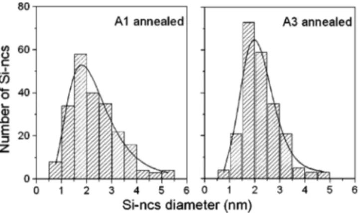
that the nanocrystals are quasispherical in shape with a mean-diameter of about 2 nm 共see Fig. 2兲. While no signifi-cant dependence of the nanocrystal mean-size on the anneal-ing treatment was detected, TEM examination shows that a more uniform nanocrystal size distribution is obtained after the A3 treatment compared with the A1 treatment.
The effect of annealing ambient on the electrical proper-ties of Si-implanted oxides has been examined through high-frequency 共1 MHz兲 C – V measurements under white light illumination conditions. The gate voltage was swept from inversion to accumulation and back to inversion at a rate of 0.5 V/s. The capacitor area was 100⫻100m2. White light illumination was used to avoid deep depletion conditions that can occur at large positive gate voltages. The structural modifications induced by a post-implantation annealing in diluted oxygen are clearly reflected in the C – V characteris-tics of 9-nm-thick Si-implanted samples reported in Fig. 3. In case of samples annealed following the A1 treatment 关Fig. 3共a兲兴, while no significant flat-band voltage shift (⌬VFB) is detected when the gate voltage is swept from⫹2 V to ⫺2 V and back to ⫹2 V, higher negative gate voltages lead to a positive voltage shift. This positive voltage shift is due to
FIG. 1. Structure of 7-nm-thick SiO2 samples implanted with 2
⫻1016
Si⫹cm⫺2at 1 keV and annealed following the A1 or A3 treatment. The mean thickness of the nanocrystalline layer thickness is about 2 nm in both cases. A3 thermal treatment leads to an increase of the control oxide by approximately 1 nm. A polysilicon film was deposited for TEM examina-tion. Dimensions were evaluated from cross-sectional HRTEM and TEM under defocused bright-field conditions共see Refs. 3 and 11兲.
FIG. 2. Nanocrystal size distribution measured from plane-view TEM im-ages of 7-nm-thick SiO2annealed according to the A1 or A3 treatment. The
number-average size共mean size兲 is around of 2 nm for both samples.
FIG. 3. High-frequency C – V curves for a 9-nm-thick oxide layer implanted with 2⫻1016Si/cm2at 1 keV and subsequently annealed following共a兲 the A1 treatment or 共b兲 the A3 treatment. 共a兲 Negative gate voltage causes electron injection into the oxide from the gate共or hole extraction from the oxide, see inset兲 and a sweep of Vgfrom accumulation (⫺Vg) to inversion
(⫹Vg) traces the curve indicated by the arrow pointing to the right.共b兲 High
positive and negative gate voltages cause, respectively, electron and hole injection into the oxide from the substrate共inset兲.
169
negative charge trapped into the oxide following electron injection from the gate electrode. If the annealing sequence uses a thermal treatment in diluted oxygen共treatment A2 or A3兲, no hysteresis appears in the C – V curves at positive or negative gate bias lower than 5 V关Fig. 3共b兲兴. Higher positive or negative gate voltages cause the C – V characteristics to shift in the direction of stored negative or positive charges, respectively. In this case, charge trapping occurs through electron and hole injection from the substrate into the oxide. We suggest that as a result of implantation damage recovery and control oxide swelling during annealing in diluted oxy-gen, the integrity of the control oxide is significantly re-stored, charging from the gate is not detectable and effective charge injection from the substrate occurs.
The effect of the A1, A2, and A3 post-implantation ther-mal treatments on the memory window of 7-nm-thick oxide layers is shown in Fig. 4. In comparison with the A1 treat-ment, the magnitude of⌬VFBas a function of the gate
volt-age sweep strongly increases after the A2 and A3 thermal treatments. It is believed that such an increase is due mainly to the improved quality of the overall oxide and enhanced thickness of the control oxide. This view is further supported by the observed gate current versus gate voltage characteris-tics under accumulation conditions of Si-implanted oxides subsequently annealed following the A1, A2, and A3 treat-ments 共inset of Fig. 4兲. It is clear that annealing in diluted oxygen leads to oxides with a strongly reduced conductivity. Finally, in view of the significant charging observed at small gate voltages共despite the large injection oxide thick-ness兲, it is inferred that the integrity of the injection oxide remains affected by the implantation process after annealing in N2/O2 ambient. It is suggested that remaining structural defects 共e.g., excess of silicon atoms兲 enhance the conduc-tivity of the injection oxide, through probably a trap-assisted direct tunneling current, thus leading to an effective charge injection into the nanocrystals at lower voltages than those required for a thermal tunnel oxide of equivalent thickness. A substantial contribution of these defects to the charge trap-ping reported herein is not excluded.
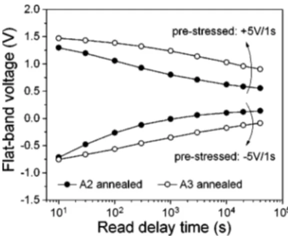
Measurements of the charge retention time at room tem-perature have been performed for 7-nm-thick A2 and A3 ox-ide layers through application of a⫾5 V gate voltage stress for 1 s. The flat-band voltage after electron 共write兲 or hole
共erase兲 injection as a function of waiting time is shown in
Fig. 5. For the A2 sample, the flat-band voltage window significantly narrows within the first 15 min and subse-quently decreases from 0.8 to 0.4 V through a waiting time of 11 h with a possible trend for stabilization. The A3 sample provides substantially larger windows for the range of times explored, with a window of about 1 V, corresponding to a waiting time of 11 h. Additional experiments performed on the same type of samples but with an additional 15-nm-thick deposited oxide reveal very similar window decay rates, thus indicating that charge loss occurs through the injection oxide and not through the control gate oxide.
Overall, appropriate midly-oxidative annealing of low-energy Si-implanted thin oxides was shown to lead to im-proved electrical characteristics pertinent to low-voltage nonvolatile memory cell applications.
This work was a part of the NEON project and was funded by the EC as GROWTH GRD1-2000-25619.
1H. I. Hanafi, S. Tiwari, and I. Khan, IEEE Trans. Electron Devices ED-43, 1553共1999兲.
2P. Normand, D. Tsoukalas, E. Kapetanakis, J. A. Van Den Berg, D. G. Armour, J. Stoemenos, and C. Vieu, Electrochem. Solid State Lett. 1, 88
共1998兲.
3M. Carrada, C. Bonafos, G. Ben Assayag, D. Chassaing, P. Normand, D. Tsoukalas, V. Soncini, and A. Claverie, Mater. Sci. Eng., B共in press兲. 4
E. Kapetanakis, P. Normand, D. Tsoukalas, and K. Beltsios, Appl. Phys. Lett. 80, 2794共2002兲.
5E. Kapetanakis, P. Normand, D. Tsoukalas, K. Beltsios, J. Stoemenos, S. Zhang, and J. van den Berg, Appl. Phys. Lett. 77, 3450共2000兲. 6P. K. Gin, V. Raireri, G. Franzo, and E. Rimini, Phys. Rev. B 65, 012110-1
共2001兲.
7A. Kalnitsky, M. I. H. King, A. R. Boothroyd, J. P. Ellul, and R. A. Hadaway, IEEE Trans. Electron Devices ED-34, 2372共1987兲.
8A. Kalnitsky, A. R. Boothroyd, J. P. Ellul, E. H. Poindexter, and P. J. Caplan, Solid-State Electron. 5, 523共1990兲.
9
J. Gyulai, in Handbook of Ion Implantation Technology, edited by J. F. Ziegler共Elsevier Science, New York, 1992兲, pp. 69–117.
10B. Schmidt, D. Grambole, and F. Herrmann, Nucl. Instrum. Methods Phys. Res. B 191, 482共2002兲.
11
G. Ben Assayag, C. Bonafos, M. Carrada, A. Claverie, P. Normand, and D. Tsoukalas, Appl. Phys. Lett. 82, 200共2003兲.
FIG. 4. Flat-band voltage shift (⌬VFB) as a function of the gate voltage round sweep for 7-nm-thick oxide layers implanted with 2⫻1016Si/cm2at
1 keV and subsequently annealed following the A1, A2, or A3 treatment. Inset: Magnitude of the dark gate current under accumulation conditions as a function of negative ramped gate voltage共1 V/s兲.
FIG. 5. Data retention characteristics of 7-nm-thick oxide layers implanted with 2⫻1016Si/cm2 at 1 keV and subsequently A2 or A3 annealed. The
magnitude of the applied gate voltage stress was⫹5 V or ⫺5 V for 1 s.