To link to this article :
DOI: 10.1002/pssr.201004392URL :
http://dx.doi.org/10.1002/pssr.201004392This is an a uthor-deposited version pu blished in: http://oatao.univ-toulouse.fr/
Eprints ID:
5864To cite this version:
Souchier, Emeline and Cario, Laurent and Corraze, Benoit and Moreau,
Philippe and Mazoyer, Pascale and Estournès, Claude and Retoux, Richard
and Janod, Etienne and Besland, Marie-Paule First evidence of resistive
switching in polycrystalline GaV4S8 thin layers.
(2011) Physica status
solidi (RRL) - Rapid Research Letters, vol. 5 (n° 2). pp. 53-55. ISSN
1862-6270
O
pen
A
rchive
T
oulouse
A
rchive
O
uverte (
OATAO
)
OATAO is an open a ccess reposi tory that co llects the work of To ulouse res earchers
and makes it freely available over the web where possible.
Any correspondence concerning this service should be sent to the repository administrator: staff-oatao@listes.diff.inp-toulouse.fr
www.pss-rapid.com
First evidence of resistive switching
in polycrystalline GaV
4S
8thin layers
Emeline Souchier1 , Laurent Cario1 , Benoit Corraze1 , Philippe Moreau1 , Pascale Mazoyer2 , Claude Estounès3 , Richard Retoux4 , Etienne Janod1
, and Marie-Paule Besland*, 1
1
Institut des Matériaux Jean Rouxel, Université de Nantes, UMR CNRS 6502, 2 rue de la Houssinière, BP 32229, 44322 Nantes, France
2
STMicroelectronics, 850 rue Jean Monnet, 38920 Crolles, France
3
CIRIMAT, UMR CNRS 5085 – UPS –INP, 118 route de Narbonne 31062 Toulouse Cedex 4, France
4
CRISMAT, UMR CNRS 6508, ENSICAEN, 6 Bd Maréchal Juin, 14050 Caen Cedex 4, France
Keywords thin films, resistive switching, GaVS, magnetron sputtering
*
Corresponding author: e-mail Marie-Paule.Besland@cnrs-imn.fr,Phone: +00 33 2 40 37 39 66, Fax: +00 33 2 40 37 39 59
Non-volatile resistive switching (RS) phenomena have recently attracted much attention because of their potential applications in next-generation non-volatile memories as alternatives to current flash memory technology. This emerging class of so-called resistive RAM (RRAM) [1] is based on functional materials that exhibit two stable re-sistive states, i.e. a high resistance state (HRS) and a low resistance state (LRS), and a reversible non-volatile resis-tive switching (RS) under electric pulses. A large variety of transition metal oxides (NiO, TiO2, SrTiO3, manganites, …) or chalcogenides are known to exhibit such RS [2–6]. It is worth noting, that all RS reported so far in these mate-rials were explained by mechanisms based on thermoche-mical or electrochethermoche-mical effects [1].
Recently we have discovered a reversible and non-volatile RS on single crystals of the AM4X8(A = Ga, Ge; M = V, Nb, Ta; X = S, Se) compounds [7–11]. The RS mechanism in these compounds is still unclear, but we did not evidence such thermochemical or electrochemical ef-fects so far. On the other hand, we have recently evidenced that the RS is driven by the electric field [10] and is asso-ciated with an unconventional electrostrictive effect [8].
Using this original RS could be of interest to build up new RRAM devices. However, prior to envision such develop-ments, two major challenges have to be tackled. The first one is to obtain stoichiometric thin layers of these chalco-genide compounds, which is non-trivial due to the high vo-latility of the chalcogen (S or Se) during the deposition. The second challenge is to recover on polycrystalline thin layers the RS properties observed only in single crystals so far. In this Letter, we focus on the deposition of thin layers of GaV4S8 and we show the existence of an electric-pulse-induced RS in theses polycrystalline samples. A detailed study of the resistive switching and associated mechanism is beyond the scope of this Letter and will appear in a sepa-rate paper.
Thin layers of GaV4S8 were deposited for the first time by RF magnetron sputtering in pure argon using a home-synthesized GaV4S8 target. Prior to the deposition, the cy-lindrical 50 mm diameter dense and stoichiometric target (90–95% of theoretical density) was made by Spark Plas-ma Sintering (SPS) technique [12] starting from a poly-crystalline GaV4S8 powder. As reported in previous works [13, 14], transfer to a thin layer of a complex ternary
mate-Recently a new type of reversible and non-volatile resistive switching was discovered in single crystals of Mott insulators AM4X8 (A = Ga, Ge; M = V, Nb, Ta; X = S, Se). Here we
re-port on the first synthesis of thin layers (thicknesses in the 100 to 1000 nm range) of GaV4S8 by RF magnetron
sputte-ring process. Energy dispersive spectroscopy, X-ray
diffracti-on and TEM analyses attest the high quality of polycrystalline GaV4S8 thin layers. Electrical measurements demonstrate that
deposited GaV4S8 thin films exhibit a non-volatile reversible
resistive switching at room temperature with writing/erasing times of ~ 10 µs and a memory window (Rhigh – Rlow)/ Rlow > 33%.
rial is favoured by soft deposition conditions. In the pre-sent study, thin layers of GaV4S8 were thus deposited on different substrates (Si(100), Si/SiO2 and Si/SiO2/Au) at low deposition pressure and RF power, respectively 40 mTorr and 60 W (i.e. 3 W cm–2). Details on optimizati-on of the depositioptimizati-on process will be published later [15].
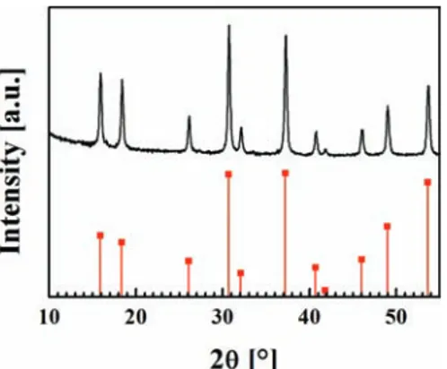
The as-deposited thin layers are sulfur deficient with a composition close to GaV4S5, as determined by Energy Dispersive Spectroscopy (EDS) and amorphous since a featureless X-ray diffraction (XRD) pattern is obtained. A one hour ex-situ annealing at 600 °C in a sulfur-rich at-mosphere restores the targeted stoichiometric composition GaV4S8 and the expected crystalline structure. The XRD pattern (Fig. 1) of the annealed thin layer (top) exhibits ex-actly the same diffraction peaks as those in the JCPDS file (n°01-070-3602) referenced for GaV4S8 (bottom). Besides, the pattern does not reveal any preferential orientation, sin-ce the relative peak intensities remain unchanged com-pared to the JCPDS file.
The annealed thin layer exhibits a granular morphology with a grain size in the 30 nm range as displayed on the Scanning Electron Microscope images (SEM) of a 1 µm thick layer after post-annealing (Fig. 2a and b). HRTEM observations performed with a JEOL 2010 FEG, STEM, at an acceleration voltage of 200 kV, are in good agreement (Fig. 2c) since TEM analyses reveal a bulk granular struc-ture with average crystallite size in the 10 nm to 30 nm range. EDS chemical analysis at the nanoscale confirms the stoichiometric composition GaV4S8.
Electron diffraction patterns were recorded for a spot size of 300 nm2, starting from the silicon substrate and the bottom interface towards the bulk layer. Nano-diffraction pattern of the bulk is consistent with a GaV4S8 phase with-out any secondary phase. Comparison of a bulk crystal-lized grain HRTEM image with simulated images [16] at various defocus and thickness values along the [110] zone axis evidences without any doubt that the obtained layer is the crystalline GaV4S8 phase (Fig. 2d). These results con-firm that the thin layers exhibit after annealing the same chemical and structural characteristics as the bulk material GaV4S8.
Figure 1 (online colour at: www.pss-rapid.com) XRD pattern of
the annealed thin layer (top) compared with the GaV4S8 JCPDS
file n°01-070-3602 (bottom).
Figure 2 SEM images of the thin layer surface (a) and cross
section (b) after the annealing step. HRTEM image of the bottom interface GaV4S8/Au (c) and comparison of HRTEM
im-age of a bulk crystallized grain in the annealed thin layer with simulated images at various focusing along the zone axis (110) (d).
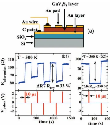
Finally, the electrical properties of GaV4S8 thin layers were investigated with Au/GaV4S8/Au/SiO2/Si MIM struc-tures (Fig. 3a). Electrical contacts on bottom and top gold electrodes were taken thanks to 10 µm diameter gold wires with conductive carbon paste on pads in the micrometer range (size 50 µm u 50 µm). The HRTEM image reveals the high quality of the MIM structures (Fig. 2c) with an abrupt transition at the bottom interface Au/GaV4S8 between the gold electrode and the GaV4S8 layer. The variation of the thin layer resistance was investigated by applying at 300 K a series of r2.5 V/10 µs pulses (red in Fig. 3b) to the device. The resistance (blue in Fig. 3b) was measured at low level (10–3 V) after each pulse. As shown in Fig. 3, each 10 µs pulse induces a writing or eras-ing resistive switcheras-ing. These characteristics are compara-ble with the 1 µs writing time achieved in Flash technology and even much better than their typical erasing times of 10 ms [17]. Figure 3(b1) displays a cycling behavior of our device between two resistance states with a switching ratio (Rhigh – Rlow)/Rlow of about 33%. This switching ratio, though not very large, is comparable with values obtained with Magnetic RAM (MRAM) at their early stage of their development [18]. Morevover the emerging Spin Torque Transfer – MRAM memories also display similar values of switching ratio [19]. In some cases, a switching ratio of 200 – 300% (see Fig. 3(b2)) can even be observed at room temperature on our GaV4S8 based device.
At this step, it is worth noting that our electrical meas-urements were performed on very basic devices using very large pads of 50 µm u 50 µm. This may complicate the evaluation of the performance of our device compared to other RRAM or MRAM devices already under industriali-sation development. For example, the large pad size leads
Figure 3 (online colour at: www.pss-rapid.com) (a) Schematic
representation of the Au/GaV4S8/Au/SiO2/Si MIM structure
used for electrical measurements with a top electrode size of 50 µm u 50 µm. (b) Examples of reversible and non-volatile re-sistive switchings obtained on a 1 µm thick GaV4S8 thin layer at
300 K with 10 µs pulses of r2.5 V with switching ratio of |33% (b1) and |250% (b2).
to small resistance values of our device that may be too small for applications. However, starting from the basic re-lation for resistance, R = UL/S, we can estimate that future
devices with pad sizes of |500 nm u 500 nm will be
around the M: in their high resistance state Rhigh. Conver-sely we expect the low resistance Rlow to be less modified by this downscaling, provided that the low resistance state results from a heterogeneous state as usually observed in other systems. This downscaling of the pad size should therefore enhance the switching ratio. We also note that, even if the downscaling will probably degrade its value, the current density required to switch between two resist-ance states is equal to 3 kA/cm2 using our current pad size, i.e. much lower size than the values given for emerging
memory devices such as MRAM (1 MA/cm2) [20] or
PCRAM (200 kA/cm2) [17].
In conclusion, we have successfully deposited GaV4S8 thin films using a low power and low pressure RF magnetron sputtering process followed by a short ex-situ annealing in sulfur rich atmosphere. The obtained stoichio-metric and crystalline thin films exhibit a granular mor-phology with grain sizes in the 10 – 30 nm range. Electrical measurements in MIM configuration with Au electrodes demonstrated that these GaV4S8 polycrystalline thin films
exhibit at room temperature a reversible resistive switching with fast writing/erasing times of about 10 µs [21], similar to the one observed initially on single crystals. All these characteristics demonstrate the potential of the AM4X8 compounds for RRAM non-volatile memory applications. Our results stand therefore as the first necessary step to-wards any further development.
References
[1] R. Waser and M. Aono, Nature Mater. 6, 833 (2007). [2] S. Q. Liu, N. J. Wu, and A. Ignatiev, Appl. Phys. Lett. 76,
2749 (2000).
[3] A. Beck, J. G. Bednorz, Ch. Gerber, C. Rossel, and D. Wid-mer, Appl. Phys. Lett. 77, 139 (2000).
[4] K. Szot, W. Speier, G. Bihlmayer, and R. Waser, Nature Mater. 5, 312 (2006).
[5] D. C. Kim et al., Appl. Phys. Lett. 88, 202102 (2006). [6] L. Goux, J. G. Lisoni, M. Jurczak, D. J. Wouters, L.
Cour-tade, and Ch. Muller, J. Appl. Phys. 107, 024512 (2010). [7] C. Vaju, L. Cario, B. Corraze, E. Janod, V. Dubost, T. Cren,
D. Roditchev, D. Braithwaite, and O. Chauvet, Adv. Mater.
20, 2760 (2008).
[8] V. Dubost, T. Cren, C. Vaju, L. Cario, B. Corraze, E. Janod, F. Debontridder, and D. Roditchev, Adv. Funct. Mater. 19, 2800 (2009).
[9] C. Vaju, L. Cario, B. Corraze, E. Janod, V. Dubost, T. Cren, D. Roditchev, D. Braithwaite, and O. Chauvet, Microelec-tron. Eng. 85, 2430 (2008).
[10] L. Cario, C. Vaju, B. Corraze, V. Guiot, and E. Janod, Adv. Mater., in press, DOI: 10.1002/adma.201002521 (2010).
[11] L. Cario, B. Corraze, E. Janod, C. Vaju, and M. P. Besland, PCT Int. Appl. PCT/EP2008/052968 (2008).
[12] C. Elissalde, M. Maglione, and C. Estournes, J. Am. Ceram. Soc. 90, 973 (2007); and PNF2 CNRS National Platform http://pnf2.dr14.cnrs.fr.
[13] M. P. Besland, H. Djani-Ait Aissa, P. R. J. Barroy, S. La-fane, P. Y. Tessier, B. Angleraud, M. Richard-Plouet, L. Brohan, and M. A. Djouadi, Thin Solid Films 495, 86 (2006).
[14] M. P. Besland, C. Borderon, S. Le Tacon, M. Cavellier, M. Richard-Plouet, D. Albertini, D. Averty, P. Y. Tessier, H. W. Gundel, L. Brohan, and M. A. Djouadi, Integrated Ferroelectrics 94, 94 (2007).
[15] E. Souchier, L. Cario, B. Corraze, P. Moreau, E. Janod, and M.-P. Besland, to be published.
[16] P. Stadelmann, Ultramicroscopy 21, 131 (1987).
P. Stadelmann, http://cimewww.epfl.ch/people/Stadelmann/ jemsWebSite/jems.html.
[17] International Technology Roadmap for Semiconductors, Emerging Research Devices (2007) – http://www.itrs.net/. [18] J. S. Modera et al., Phys. Rev. Lett. 74, 3273 (1995).
N. Nishimura et al., J. Appl. Phys. 91, 5246 (2002). [19] Y. Huai et al., J. J. Appl. Phys. 45, 3835 (2006).
Y. Huai, AAPPS Bulletin 18, 33 (2008). S. Mangin et al., AAPPS Bulletin 18, 41 (2008). [20] C. Chapert et al., Nature Mater. 6, 813 (2007).
[21] E. Souchier, M.-P. Besland, B. Corraze, L. Cario, E. Janod, and J. Martial, French patent, 09/51744, March 2009.