O
pen
A
rchive
T
OULOUSE
A
rchive
O
uverte (
OATAO
)
OATAO is an open access repository that collects the work of Toulouse researchers and
makes it freely available over the web where possible.
This is an author-deposited version published in :
http://oatao.univ-toulouse.fr/
Eprints ID : 18256
To link to this article :
DOI: 10.1109/EMCCompo.2017.7998085
URL :
http://dx.doi.org/10.1109/ECMSM.2017.7945864
To cite this version :
Boyer, Alexandre and Gonzalez Sentis, Manuel Antero
and Ghfiri, Chaimae and Durier, André Modeling methodology of the
conducted emission of a DC-DC converter board. (2017) In: EMC Compo
2017 (The 11th International Workshop on the Electromagnetic
Compatibility of Integrated Circuits), 4 July 2017 - 8 July 2017 (Saint
Petersburg, Russian Federation).
Any correspondence concerning this service should be sent to the repository
administrator:
[email protected]
Study of the thermal aging effect on the conducted
emission of a synchronous buck converter
A. Boyer
1(1) CNRS, LAAS, 7 avenue du colonel Roche Univ. de Toulouse, INSA, LAAS, F-31400 Toulouse,
France [email protected]
M. A. Gonzalez Sentis
2, C. Ghfiri
1,2, A. Durier
2 (2) IRT Saint-Exupéry, 118 route de Narbonne, CS 44248,Toulouse, France
[email protected], [email protected]
Abstract—This paper studies the impact of the accelerated
thermal aging on the conducted emission produced by a synchronous buck converter. The most degraded devices mounted on the DC-DC converter are identified and modeled in order to simulate the evolution of conducted emission and anticipate risks of non-compliance to emission requirements.
Keywords— DC-DC converter; electromagnetic emission; accelerated aging; degradation modeling
I. INTRODUCTION
Because of their high power efficiency, switch-mode power supplies (SMPS) are widely used in electronic applications [1]. However, one main drawback of SMPS is the noise produced by the switching activity, responsible for conducted and radiated electromagnetic emission (EME). Therefore, the management of the parasitic emission of SMPS is a frequent topic in the literature on electromagnetic compatibility (EMC). Numerous papers dealt with the origin and the modeling of EME, and also the development of design guidelines to improve these issues [2] [3]. Several recent studies presented the long-term behavior of SMPS. As a result of the degradation of the electrolytic capacitors which are used to filter the output voltage of SMPS, an increase of ripple in the output voltage of SMPS was illustrated in [4] [5]. Another consequence is the increase of EME, as shown in [6], which is associated with the degradation of filtering passive devices.
This work is an extension of [6], where the different devices that form a synchronous buck converter (capacitor, inductor, ferrite bead, diode, power MOSFET) are stressed thermally. Their impact on the evolution of EME is studied by simulation. Besides, the study presented in [6] focuses only on the conducted emission (CE) at the output of the DC-DC converter. This work includes the measurement and the simulation of the CE at the input of the DC-DC converter. the paper is organized as follows: the first section describes the studied DC-DC converter, the tested devices and the accelerated aging method. The second section presents the experimental results of characterization of stressed devices and their modeling. In the last section, the model of stressed devices are used to simulate the effect of thermal aging on the CE produced by the DC-DC converter. The influence of aging of different filtering passive devices is compared.
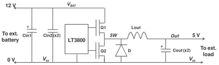
II. PRESENTATION OF THE CASE STUDY A. Description of the DC-DC converter
The studied synchronous buck converter is mounted on a 55x58 mm four-layer board. This type of circuit is one of the major contributor of conducted and radiated emission in electronic systems. A simplified schematic of the converter is presented in Fig. 1. It is based on the LT3800 controller from Linear Technology, configured in step-down operation to convert the 12 V voltage provided by a battery into a 5 V regulated voltage for a maximum current of 10 A. This circuit drives the gates of two power NMOSFET (Q1, Q2) mounted in D2PAK package. A Schottky diode (D) is mounted in parallel to Q2. The switching frequency is set to 200 KHz. An external dummy load is connected to the regulated output node (Out) during the CE characterizations. The capacitors Cin1 and
Cin2 filter the CE at the power supply input VBAT, and Lout and
Cout devices the regulated output Out. The list of components
mounted on the converter board is given in Table I.
12 V ! ! To ext. load LT3800 Lout D !"# 5 V To ext. battery $%&' $(( 0 V )* $(( Q1 Q2 Cout (x2) Cin1 Cin2 (x2)
Fig. 1. Electrical diagram of the studied DC-DC converter
The characterization of the CE produced by the DC-DC converter follows the recommendations given by CISPR16 standard. The measurements are done in a semi-anechoic chamber. The DC-DC converter is connected to the power supply source through a 1.2 m cable, placed at 5 cm over a large conductive ground reference plane, and (50 !H+5 ")//50 " LISN compliant to CISPR16-1-2 to characterize CE that propagates along the power supply cable. Additionally, a 150 " probes, defined according to the IEC61967-4 standard [7], is placed at the regulated output Out to characterize the CE along the DC-DC converter output. Both measurements are done between 9 kHz and 100 MHz.
A SPICE compatible model has been developed to simulate the CE produced by the DC-DC converter. The description and the validation of the model is presented in [8]. This work is supported by the IRT Saint-Exupéry Robustesse Electronique project sponsored by Airbus Operations, Airbus Group Innovations, Continental Automotive France, Hirex Engineering, Nexio, Safran Electrical & Power, Thales Alenia Space France, Thales Avionics and the French National Agency for Research (ANR).
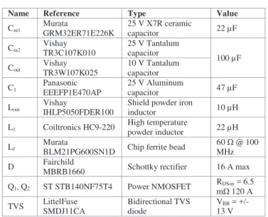
B. Overview of tested components
The characteristics of the filtering passive devices, power MOSFET and Schottky diode mounted on the DC-DC converter are given in Table I. Additional components, which are not actually mounted on the converter board during CE characterization, are also tested. They are often mounted on SMPS for EMC purpose: an aluminium electrolytic capacitor C1, a high temperature powder inductor L1, a chip ferrite bead
Lf. These devices could be added on the DC-DC converter for
filtering purpose. Moreover, a bidirectional Transient Voltage Suppressor (TVS) diode, dedicated to filter out transient overvoltage coupled on the power supply input, is also studied. Most of the components operates on the temperature range -55°c to 125°c, except the aluminium capacitor given up to 85°c and the high temperature inductor which can operate up to 155°c without any derating.
TABLE I. TESTED DEVICE CHARACTERISTICS
Name Reference Type Value
Cin1 Murata GRM32ER71E226K 25 V X7R ceramic capacitor 22 µF Cin2 Vishay TR3C107K010 25 V Tantalum capacitor 100 µF Cout Vishay TR3W107K025 10 V Tantalum capacitor C1 Panasonic EEEFP1E470AP 25 V Aluminum capacitor 47 µF Lout Vishay IHLP5050FDER100
Shield powder iron
inductor 10 µH L1 Coiltronics HC9-220 High temperature
powder inductor 22 µH Lf Murata
BLM21PG600SN1D Chip ferrite bead
60 " @ 100 MHz D Fairchild
MBRB1660 Schottky rectifier 16 A max Q1, Q2 ST STB140NF75T4 Power NMOSFET RDSon = 6.5
m" 120 A TVS LittelFuse SMDJ11CA Bidirectional TVS diode V13 V BR = +/-
For each type of device, five samples are tested. Depending on the nature of the component, different measurements are made to characterize the effect of aging. The impact of aging on linear passive devices is observed through the evolution of their impedance profile in frequency domain. S-parameter measurements are performed using a vector network analyzer to extract the impedance profile of passive devices between 9 kHz and 1 GHz. I(V) measurements of Schottky and TVS diodes and power NMOSFET are made with a high power pulse curve tracer Tektronix 371. The voltage dependence of their junction and gate capacitances is also extracted with the curve tracer Agilent B1505A.
C. Accelerated aging
Accelerated aging test is always applied to obtain reliability data of electronic components in a short period. In order to accelerate the converter aging, The passive devices listed in Table I are placed two weeks (336 h) in a thermal oven, which regulates the ambient temperature at 150 °C. The stress temperature in this test could ensure a relative short
aging time without damaging the tested devices definitively. The passive devices are characterized before the stress, after one week (168 h) and at the end of the stress (336 h). Moreover, three converter boards are also placed in the thermal oven. They are biased and loaded by 10 " resistors. III. CHARACTERIZATION AND MODELING OF THERMAL STRESS
EFFECT ON DEVICES A. Experimental results
Table II provides a summary of the extent of the degradations observed on the tested devices after the thermal stress. The degradation concerns mainly the filtering devices. Two passive devices are seriously degraded: aluminium capacitor and iron powder inductor. The other devices are either unaltered or their characteristics are partially modified. The following paragraphs provide more details about the experimental results.
TABLE II. SUMMARY OF OBSERVED DEGRADATION ON TESTED DEVICES
Name Type Stress effect
Cin1 25 V X7R ceramic capacitor None
Cin2 25 V Tantalum capacitor
Moderate Cout 10 V Tantalum capacitor
C1 25 V Aluminum capacitor High
Lout Shield powder iron inductor High
L1 High temperature powder inductor None
Lf Chip ferrite bead Moderate
D Schottky rectifier Moderate Q1, Q2 Power NMOSFET Moderate
TVS Bidirectional TVS diode Moderate
Fig. 2 presents the measured evolution of the impedance of the aluminium electrolytic capacitor. A decrease of the capacitance value is observed but the most significant effect for EMC is the increase of its equivalent serial resistance (ESR). For CE point of view, it has a major impact in low frequency. This trend is confirmed by previous study [4]. As observed in [6], the ESR increases slowly at the beginning of lifetime, but this trend speeds up at the end of lifetime.
Fig. 2. Evolution of the impedance of the electrolytic capacitor C1 before and
after thermal aging
Other capacitor types do not suffer such major degradations. Ceramic capacitors are unaffected by the thermal stress. This result confirm their high robustness pointed out in numerous publications and technical notes [9].
A small but significant increase of the ESR of tantalum capacitors is visible between 10 kHz and 1 MHz as shown in Fig. 3.
Fig. 3. Evolution of the impedance of the output tanalum capacitor Cout after
thermal aging
The iron powder inductor is also considerably degraded by the thermal stress, as shown in Fig. 4. As observed in [6], the self-resonant frequency and the quality factor decline, and the impedance reduces between 4 and 100 MHz. This change can have a major impact on its filtering performance. This evolution is explained by a degradation of the organic binding material of the powder, which leads to an increase of core loss caused by the thermal stress [10]. As observed in [6], the degradation rate is more important at the lifetime beginning.
Fig. 4. Evolution of the impedance of the iron powder inductor Lout after thermal aging
Fig. 5. Evolution of the impedance of the ferrite bead Lf after thermal aging
The impact of thermal aging can be minimized if powder inductors without organic binder are used, such as the reference HC9-220. As claimed by the manufacturer, this device can operate at high temperature (at least up to 150°c) without any significant changes in its impedance profile. A significant decrease of the impedance of the ferrite bead, especially its real part, is also measured, as shown in Fig. 5. However it remains modest enough to induce a serious degradation of its filtering performances.
The I(V), C(V) and Z(f) tests done on the Schottky diode shows that only the on-resistance changes, without any changes of the forward voltage and junction capacitance. The increase of the Ron resistance after 336 hours of thermal stress is comprised between 50 and 100 % depending on the tested sample (Fig. 6). Nevertheless, this increase remains modest and has no significant effect on EMC.
Fig. 6. Evolution of the I(V) curve of the Schottky diode
Fig. 7. Evolution of the I(V) curve of the TVS diode
The TVS diode remains functional after this thermal stress but a gradual evolution due to thermal aging is visible on the I(V) characteristic of the TVS diode, as shown in Fig. 7. It is mainly due to an increase of the on-resistance. A little increase of the breakdown voltage is also visible. The junction capacitance is not affected. Depending on the tested sample, the relative increase of on-resistance from 40 to 200 %. Although this evolution has no consequence on CE, the performances of the TVS to suppress transient disturbances are partially degraded.
The I(V) curves of the power NMOSFET are also partially modified after the thermal aging, as shown in Fig. 8. This effect can be explained by a little increase of the threshold
voltage of the MOSFET. However, the on-resistance remains unchanged, as the gate and junction capacitances. This change has no major consequences on CE.
Fig. 8. Evolution of the I(V) curve of the power NMOSFET
B. Passive device model extraction
In order to simulate the effect of device degradation on the evolution of CE produced by the DC-DC converter, electrical model of aged devices are constructed from measurements done after thermal stress. Only filtering devices (capacitors and inductors) are addressed.
Fig. 9 presents the equivalent electrical model of the tantalum capacitor Cout before stress. The same structure can
be used to model aluminium capacitor. As shown by VNA measurement results, the thermal stress affects mainly the ESR of these capacitors. An analysis of measurement results and the electrical models show that the same model topology can be kept to model stressed capacitors. Only the elements dedicated to the ESR modeling have to be updated to take into account the effect of the thermal stress. The ESR is modeled by a series of parallel R-C cells in order to simulate its non linear evolution in frequency domain. The number of R-C cells and R and C values are adjusted to fit simulated and measured ESR. Fig. 10 present comparisons between measured and simulated impedances of aluminium capacitors, before and after 336h thermal stress, which show a good agreements.
+),-./012-345652212-,78-9122(:
Fig. 9. General structure of the electrical model of aluminium and tantalum capacitor
Fig. 10. Comparison between measurement and simulation of the impedance of a 25 V 47 µF aluminium capacitor C1 before and after 336h thermal stress
Fig. 11 describes the electrical model of the iron powder inductor Lout before stress. An analysis of measurement results
and the electrical models show that the same model topology can be kept. Only the parallel parasitic capacitance and the loss resistance Rp_L1 have to be modified to take into account for the effect of the thermal stress. Their values are adjusted to fit simulated and measured impedance. Fig. 12 presents comparisons between measured and simulated impedances of the iron powder inductor, before and after thermal stress.
Fig. 11. Electrical model of the iron powder inductor Lout1 before thermal
stress
Fig. 12. Comparison between measurement and simulation of the impedance of th iron powder inductor Lout before and after 336h thermal stress
IV. STUDY OF THE INFLUENCE OF COMPONENT AGING ON THE EVOLUTION OF CONDUCTED EMISSION
In this part, the models of stressed component are used to simulate the evolution of the CE of the DC-DC converter due to thermal stress. A model dedicated to the simulation of the DC-DC converter has been built and validated previously [8].
Firstly, the effect of the thermal stress on the DC-DC converter with the original design described in Fig. 1 is analyzed by simulation. The simulation results are then compared with CE measurement done on stressed converters to validate the relevance of the model. Secondly, the model is used to study the evolution of CE if other filtering devices were mounted on the DC-DC converter. To facilitate comparison between measured and simulated CE, only spectrum envelops are displayed.
A. Simulation of the effect of thermal stress on the conducted emission of the DC-DC converter
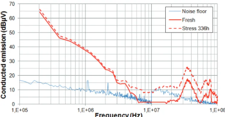
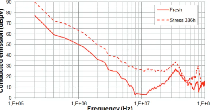
Figs. 13 and 15 present the CE measured at the input and output of the DC-DC converter, before and after thermal stress. The same trends are observed on the three tested converters. An important increase of the output CE is measured between 4 and 100 MHz, which reaches up to 15 dB. However, the input CE remains constant after aging. On both measurement results, a resonance is clearly visible at 34 MHz. It is due to the resonance loop formed by the junction capacitances of the Schottky diode and the MOSFETs and the parasitic inductances of the input decoupling capacitors and PCB traces. This resonance frequency remains stable after aging since these parasitic capacitances and inductances are unaffected by the thermal stress, as confirmed by experimental results shown in part III.
Figs. 14 and 16 present the simulated CE at the input and output of the DC-DC converter, with the models of either the sound or stresses tantalum capacitors and iron powder inductor. The influence of aging of the other components (ceramic capacitor, Schottky diode, MOSFET) is neglected. The simulation reproduces the measured evolution of the CE. A slight increase (less than 1 dB) is predicted below 1 MHz but it remains too small to be detectable in measurement. This increase is due to the moderate increase of the ESR of the tantalum capacitor Cout. Above 4 MHz, an increase that can
reach up to 15 dB is observed which is related to the degradation of the inductor Lout. The model also confirms the
invariability of the input CE, which is dependent on the input filtering capacitors. In spite of the moderate degradation of tantalum capacitor Cin2, the ceramic capacitors Cin1 provide a
sufficiently small ESR that compensates completely the ESR increase of the tantalum capacitor.
Fig. 13. Evolution of the measured output conducted emission spectrum
Fig. 14. Evolution of the simulated output conducted emission spectrum
Fig. 15. Evolution of the measured input conducted emission spectrum
Fig. 16. Evolution of the simulated input conducted emission spectrum
B. Prediction of the effect of thermal stress on conducted emission with different filtering devices
The model confirms the evolution of the CE due to thermal aging, which is mainly related to the gradual degradation of filtering devices. No increase of the input CE is visible since ceramic and tantalum capacitors are robust to thermal stress, contrary to iron powder inductor. The rise of its losses alters the CE at the output side of the DC-DC converter.
The model of the DC-DC converter can be reused to predict the evolution of the CE if other capacitors and inductors are mounted. Three scenarios are tested. In the first scenario, the CE is simulated if only aluminium capacitors C1
were mounted on the DC-DC converter board. The evolutions of input and output CE are presented in Figs. 17 and 18. Compared to the evolution shown in the previous part, an important rise of the input and output CE is observed up to 20
MHz, because of the serious degradations of aluminium capacitors. Above 20 MHz, the increase of the output CE is related to the degradation of iron powder inductor. This result confirms that aluminum capacitors should not be used for applications in harsh environments, otherwise significant increase of CE may arise.
Fig. 17. Prediction of the evolution of the output conducted emission spectrum if only aluminium capacitors are mounted
Fig. 18. Prediction of the evolution of the input conducted emission spectrum if only aluminium capacitors are mounted
In the second scenario, the input CE is simulated if only tantalum capacitors were mounted. Only a slight increase of the input CE is observed below 1 MHz (Fig. 19), which reaches nearly 2 dB at the fundamental frequency. Even if ceramic capacitors were replaced by tantalum capacitors, the CE evolution would remain reasonable.
Fig. 19. Prediction of the evolution of the input conducted emission spectrum if only tantalum capacitors are mounted
In the last scenario, the output CE is simulated if the high temperature inductor L1 replaces the iron powder inductor Lout.
The simulation confirms that the robustness of this inductor to thermal stress prevents the output CE increase above 4 MHz.
V. CONCLUSION
This paper has presented a study about the influence of thermal stress on the conducted emission produced by a synchronous buck converter. The effect of thermal stress on various passive and active devices (capacitors, inductors, ferrite bead, MOSFET, Schottky and TVS diodes) was characterized and modeled to simulate the evolution of conducted emission. The model reproduced correctly the measured evolution. It was also used to predict how the conducted emission would change if other filtering devices were used. This type of modeling and simulation approach is helpful to anticipate the risks of non-compliance of electronic equipments to EMC requirements after several years of operation.
,1;161<91(-[1] C. Basso, Switch-Mode Power Supplies SPICE Simulations and Practical Designs, McGraw Hill Professional, 2008.
[2] K. Kam, D. Pommerenke, A. Bhargava, C. Lam, R. Steinfeld, F. Centola, “Analysis and Mitigation Techniques for Broadband EMI from Synchronous Buck Converter”, IEEE Electromagnetic Compatibility Magazine, Vol. 1, Quarter 3, 2012.
[3] K. Mainali, R. Oruganti, “Conducted EMI Mitigation Techniques for Switch-Mode Power Converters: A Survey”, IEEE Transactions on Power Electronics, Vol. 25, No 9, September 2010.
[4] A. Lahyani, P. Venet, G. Grellet, P.J. Viverge, “Failure Prediction of Electrolytic Capacitors During Operation of a Switchmode Power Supply,” IEEE Trans. Power Electr., vol. 13, no 6, Nov. 1998.
[5] Y. Chen. “Electrolytic capacitor failure prediction of lc filter for switching-mode power converters”, Industry Applications Conference, 2005. Fortieth IAS Annual Meeting, 2(2):1464 – 1469, Oct 2005. [6] H. Huang, A. Boyer, S. Ben Dhia, “Analysis and Modelling of Passive
device degradation for a long-term electromagnetic emission study of a DC-DC converter”, 26th Eur. Symp. on Reliability of Electron Devices, Failure Physics and Analysis (ESREF 2015), Oct. 2015.
[7] IEC 61967-4 – edition 1.1: Integrated circuits - Measurement of electromagnetic emissions, 150 kHz to 1 GHz - Part 4: Measurement of conducted emissions – 1 "/150 " direct coupling method, 2006-07. [8] A. Boyer, M. G. Sentis, C. Ghfiri, A. Durier, " Modeling methodology
of the conducted emission of a DC-DC converter board", submitted to EMCCompo 2016.
[9] Knowles, Application note AN0006, “Capacitance Ageing of Ceramic Capacitors,Explanation of the natural ageing process resulting in logarithmic loss of Capacitance”, Technical report
[10] J.Kindmark and F. Rosen, “Powder Material for Inductor Cores, Evaluation of MPP, Sendust and High flux core characteristics”, Master of Science Thesis, Chalmers University of Technology, Geoteborg, Sweden, 2013.