HAL Id: hal-01935110
https://hal-univ-rennes1.archives-ouvertes.fr/hal-01935110
Submitted on 7 Dec 2018
HAL is a multi-disciplinary open access archive for the deposit and dissemination of sci-entific research documents, whether they are pub-lished or not. The documents may come from teaching and research institutions in France or abroad, or from public or private research centers.
L’archive ouverte pluridisciplinaire HAL, est destinée au dépôt et à la diffusion de documents scientifiques de niveau recherche, publiés ou non, émanant des établissements d’enseignement et de recherche français ou étrangers, des laboratoires publics ou privés.
Impact of the post-thermal annealing on OFETs using
printed contacts, printed organic gate insulator and
evaporated C-60 active layer
Zhi Tao, Tayeb Mohammed-Brahim, Wei Lei, Maxime Harnois, Emmanuel
Jacques
To cite this version:
Zhi Tao, Tayeb Mohammed-Brahim, Wei Lei, Maxime Harnois, Emmanuel Jacques. Impact of the post-thermal annealing on OFETs using printed contacts, printed organic gate insula-tor and evaporated C-60 active layer. Solid-State Electronics, Elsevier, 2018, 150, pp.51-59. �10.1016/j.sse.2018.10.011�. �hal-01935110�
Impact of the post-thermal annealing on OFETs using printed contacts, printed
organic gate insulator and evaporated C60 active layer
Zhi Taoa,b,*, Tayeb Mohammed-Brahima, Wei Leib, Maxime Harnoisa, Emmanuel Jacquesa
a
Institut d’électronique et des Télécommunication de Rennes, UMR CNRS 6164, Université de Rennes 1, Campus de Beaulieu, 35042 RENNES Cedex (France)
b
School of Electronic Science and Engineering, Southeast University, Nanjing 210096, People’s Republic of China
Corresponding author: phone: +33 0663445554; E-mail: tz-0001@163.com
Present address: Institut d’électronique et des Télécommunication de Rennes, UMR CNRS 6164, Université de Rennes 1, Campus de Beaulieu, 35042 RENNES Cedex (France)
Abstract
Towards fully printed organic electronics, bottom-gate, bottom contacts fullerene based organic FETs (OFETs) are fabricated using inkjet printing drop-on-demand technology for the deposition of gate contact, organic gate insulator and source and drain contacts. The last layer of this structure that is the semiconducting fullerene C60
film, is deposited by thermal evaporation at ambient temperature. Using physical and electrical analysis, the electrical performances are optimized by studying the effect of the thickness of the C60 film and of the post-thermal annealing of the OFET. A
quantitative relationship between the crystalline structure of the C60 semiconducting
layer (grain size and surface roughness) and the electrical performance of the OFETs is demonstrated. The best performance as determined from the values of the electrical parameters of the OFETs are obtained for 90 nm thick C60 film and after an annealing
of the OFET at 200°C. The answer of present nearly fully printed OFETs to a voltage pulse applied to the gate lead to a switching time of 13 ms, and then to application frequency of some 10Hz. This result opens the way to potential main application in electronic circuits for the treatment of analog signals coming from the human body activities.
Keywords: inkjet printing drop-on-demand, Organic FET, physical
1 Introduction:
Now, flexible electronics becomes a major research domain due to the fast-growing market. The overall revenue of wearable technology was $38 billion in 2017 and it is expected to grow over $85 billion in 2022 [1]. The dominant sectors will be the healthcare and medical, fitness and wellness. The main requirement for flexible or even stretchable devices is the use of ultra-flexible materials. The first parameter indicating the flexibility of a material is its Young modulus. With their very low Young modulus, organic materials are considered fitting perfectly the requirement of flexibility. The main purpose is then to fabricate electronic devices using organic materials.
P-type Organic Field Effect Transistors (OFETs) have exhibited the better performance compared with n-type OFETs. However, for the most efficient electronics, both N-type and P-type OFETs are demanded. Then, intense research is done to increase the performance of N-type OFETs. Among n-type organic semiconductors, fullerene shows great potential with reliable common field effect mobility close to 1 cm2V-1s-1 [2]. The field effect mobility has been even higher, 6 cm2V-1s-1, by using fullerene deposited at 250°C by hot-wall epitaxy [3]. Fullerene OFET presents not only interesting mobility but also a high electrical stability. By changing the gate insulator, Zhang et. al [4]succeeded in fabricating fulle ren e b a s e d O F E T with high electrical stability under continuous polarization. The drain current degradation was about 3.1% during 2 h under bias stress. These performances were obtained thanks to the use of photolithography process and high cost deposition techniques. Indeed, to fabricate organic transistors, technologies involve usual deposition and photolithography techniques [5] and other new ones as deposition in solution by different ways spin-coating, drop-casting and printing using shadow hard or software masks [6,7].
Considering the huge promising market, the chosen technology has to be made easily at the lowest cost possible, on large area and at enough low temperature to be compatible with flexible substrate. Deposition in solution, particularly printing technology, fulfill these requirements and become now more and more used. Among several printing technologies, inkjet printing drop-on-demand technology is more promising [8,9]. More than the common properties of these techniques, low cost and easy to use, inkjet printing adds the low consumption of materials, the well-controlled process leading to considerable reproducibility and the possibility to fabricate very small features.
Present work fits with the perspective of low cost and easy processed fully organic electronics, by trying to fabricate bottom-gate, bottom contacts fullerene based OFETS using inkjet printing drop-on-demand technology. Our previous works [10,11] optimized the printing of silver on glass as gate contact and on photoresist SU8 as source and drain contacts and the printing of this photoresist SU8 as gate insulator. The present work focuses on the deposition of fullerene C60 by thermal
combined with photolithography processing, the solution process such as printing leads to thicker deposited films. Then, in a bottom-gate, bottom contacts structure of the OFETs, the high aspect ratio between the drain and source contacts and the gate insulator imposes the use of thick semiconducting active layer. Present work will highlight the influence of the thickness of the C60 active layer on the performance of
nearly fully printed C60 based bottom gate – bottom contacts OFETs.
The effect of the post-thermal annealing on the as-fabricated OFETs with different thickness of C60 active layer will be studied also. In our knowledge, no such
work, combining the studies of the thickness and the post-thermal annealing on C60
OFETs, was previously done. It will lead to determine the optimum OFET’s processing parameters.
Consequently, for the first time, a quantitative relationship between the crystalline structure of the C60 active layer (grain size and surface roughness) and the
electrical performance of the OFETs is demonstrated.
2 Experimental
2.1 Transistor fabrication and characterization
Fig.1 shows a schematic cross-section of the C60 OFET fabricated following
bottom gate and bottom contacts geometry. This figure highlights the problematic of the high aspect ratio between the drain and source contacts and the gate insulator. The thickness of the active layer has to be enough to insure good coverage between the source and drain contacts.
.
Fig. 1: Cross-section of the C60 OFETs using bottom gate and bottom contacts geometry. The figure highlights the problematic of the high aspect ratio between the drain and source contacts and the
gate insulator
As illustrated in Fig.2, after cleaning the glass substrate with acetone, ethanol, and deionized water for 10 mins sequentially, the silver gate electrode was printed on the substrate (keeped at 50°C) with a thickness of 200nm using 256 nozzles Q-class printhead (Dimatix©)(Fig2.b). Before spin coating the gate insulator layer, the substrate with silver gate electrodes is baked at 110°C for 30min allowing nanoparticules based ink sintering. Then, 1.2μm thick uncrosslinked SU8 2000 series photoresist (Bisphenol A Novolak epoxy; MicroChem) is spin-coated at a speed of 4500r/min during 60 seconds (Fig2.c). This layer will be used as polymeric gate insulator. After UV exposure and development (SU8 micro Dev, MicroChem), the SU8 layer was baked at 115°C during 15min.The baked SU8 layer is then submitted to 2mins
UV-Ozone treatment to adjust SU8 wetting behavior [10-12] ready for the printing of source and drain contacts. Drain and source electrodes were printed at 50°C using different patterns (width of the electrodes W=4000µm, distance between the electrodes L=150µm, and the thickness of the electrodes D=205nm in Fig2.d). Finally, C60 film is thermally evaporated as the active layer of the transistor at room
temperature under vacuum (2x10⁻⁷ mbar) with a constant deposition rate of 0.15A/s (Fig2.e).
The C60 active layer was deposited with four different thicknesses, 60 nm, 90 nm,
125nm and 250 nm in the purpose to study the effect of its thickness. The OFET is then characterized electrically, as deposited and after annealing at 3 different temperatures, 160°C, 200°C and 250°C, during 5 mins. Electrical characterization was performed in dark and under nitrogen atmosphere using a 2636A Keithley (Fig2.f).
Fig. 2: Fabrication process of C60 OFET
2.2 Morphological characterization and topography parameters extraction of the C60
active layer.
In the purpose to study the effect of the temperature during the final annealing of the OFET, the morphology of the C60 active layer was analyzed using Atomic Force
Microscopy (AFM). An Atomic Force Microscope (AFM VEECO Di Caliber) was utilized in tapping mode on an area of 1x1 µm2. To describe the topography of the surface, we use the Power Spectral Density Function (PSDF). Its formulation is given by [26]:
(1)
Here S is the 2-dimensional PSDF, L2 is the scanned surface area, N is the number of data points in both X and Y direction of scanned area, hmn is the surface profile
height at position (m,n), fx and fy are the spatial frequencies in X and Y directions
respectively, ΔL is the sampling interval. Based on the AFM images (1µmx1µm), the RMS roughness (σ) and the lateral correlation length (τ) were calculated from these PSDF functions (support files). Besides, the lateral correlation length (τ) is related to the grain size.
2.3 Electrical parameter extraction
As the most important electrical parameters, the field effect mobility μ (cm2.V.s-1), the sub-threshold slope SS (V.decade-1), the threshold voltage VTH (V), the contact
resistance Rc (Ω), the minimum off-state current Ioff (A), the on/off current ratio Ion/Ioff
are utilized to evaluate the performance of the thin-film transistor.
In linear regime, µ, SS and VTH are calculated from the equation 2 of the drain
current ID (VDS << (VGS-VTH)):
(2)
Where the W, L and Cins are the width, the length of the channel and the capacitance
of the gate insulator per area unit, respectively. The slope of ID-VGS curve at constant
VDS is the transconductance gm given by:
(3)
The threshold voltage VTH is the gate voltage axis intercept of ID-VGS curve
plotted in linear part. The field effect mobility µ is deduced from the extraction of gm.
The subthreshold slope SS is extracted from ID-VGS curve plotted in
semi-logarithmic scale using:
(4)
The contact resistance Rc is calculated from the equation of the drain-source
resistance RDS:
(5)
where Rc is the contact resistance, assumed similar for both source and drain
contacts.
3 Results and discussions
3.1 Effect of the semiconductor annealing temperature on the morphology of the C60
thin film on the OFET.
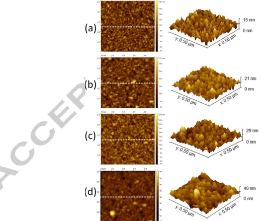
3.1.1 Morphology of C60 active layer as a function of the annealing temperature.
morphology of its C60 active layer, the thickness of this layer was fixed at 125nm. The
morphology was studied as deposited and after annealing at 160°C, 200°C, 250°C. As illustrated in Fig.3, the 2D, 3D and line scan AFM images of C60 thin film as
deposited and after annealing at 160°C, 200°C and 250°C exhibit that C60
morphology depends on the annealing temperature. From the 2D AFM images, the surface roughness increases and the number of grains decreases in the same area when the annealing temperature increases. Quantitatively, the RMS roughness s and grain size t were calculated using the equation (1) and reported in Table 1.
Table 1: RMS roughness and grain size calculated using PSDF formulation (1)
Annealing Temperature (°C) Roughness (nm) Grain size (nm) As-deposited 1.42 4.72 160 1.75 7.70 200 1.91 13.46 250 2.72 14.16
Morphological parameters (roughness and grain sizes values) continuously increase when annealing temperatures increase. Furthermore, the grain size increases more when such temperature is below 200°C than between 200°C and 250°C.
Fig. 3: 2D ( ) AFM images, corresponding 3D enlarged ( ) (a) as-deposited; and after annealing at 160Cº (b), 200°C (c) and 250°C (d)
3.2.1 OFET with 125 nm thick C60 active layer as a function of the annealing
temperature
and after an annealing at 3 different temperatures, 160°C, 200°C and 250°C. All the OFETS have the same size (channel width and length equals to 4000 µm and 150µm, respectively).
Fig.4: (a)Mean transfer characteristics (VD=20V) and (b) output characteristics (VG=20V) of several
OFETs having the same size (channel width W=4000 µm, channel length L=150 µm) and 125 nm thick C60 active layer, measured as-fabricated and after annealing at 160°C, 200°C and 250°C.
All the OFET’s parameters such as threshold voltage, subthreshold slope, field effect mobility, on-current, improve when the annealing temperature increases. The value of these parameters is reported in Table 2 and plotted as a function of the annealing temperature in Fig. 5a.
Table 2
Main mean electrical parameters of several OFETs having the same size (channel width W=4000 µm, channel length L=150 µm) and 125 nm thick C60 active layer, measured as-fabricated and after
annealing at TA=160°C, 200°C and 250°C. VTH is the threshold voltage, SS the subthreshold slope, µ
the field effect mobility, RC the contact resistance, µ after RC the mobility after correction by RC, Ioff is
the minimum current and Ion/Ioff is the ratio between the maximum current and the minimum current
TA (°C) VTH (V) SS (V/dec) µ (cm2/V.s) Rc () µ after Rc (cm2/V.s) Ioff (A) Ion/Ioff Unannealed 19.3 9.3 5.3x10⁻⁵ 8x10⁶ 5.8x10⁻⁵ 1.6x10⁻¹¹ 125 160 20 7 4.2x10⁻³ 2x10⁶ 4.47x10⁻³ 3.4x10⁻¹¹ 4.7x10³ 200 11.2 4 1.44x10⁻² 1.7x10⁶ 1.46x10⁻² 2x10⁻¹⁰ 2.85x10³ 250 6.2 6.2 1.46x10⁻² 2x10⁶ 1.5x10⁻² 2x10⁻⁹ 270
Table 2 highlights that the main electrical parameters (i.e., threshold voltage, subthreshold slope, mobility) are strongly impacted by annealing temperature (especially bellow 200°C). It seems that these electrical parameters are governed by the grain size.
The contact resistance decreases after the annealing at 160°C and then stabilizes. Its value stays much lower than the channel resistance and then the corrected mobility by removing the effect of the contact resistance, does not change drastically. This conclusion was expected due to the starting linear increase of the drain current as can be observed in the output characteristics. Moreover, the off-current increases when the
annealing temperature increases. The increase seems to be due to the improvement of the active layer after annealing and then to better conductive layer. Considering these preliminary observations, it seems that the optimum annealing temperature is 200°C. The different parameters after this annealing are similar to the 250°C annealing ones. Moreover, the on-current to off-current ratio is higher that its value after 250°C annealing.
To understand the behavior of the main parameters depending on the annealing temperature, we can try to highlight a relationship between the AFM and the electrical characterizations. The mobility and the grain size present similar behavior as shown in Fig. 5b. Both, mobility and grain size strongly increase when temperature increases until 200°C and a little bit when the grain size increases between 200°C and 250°C. The subthreshold slope SS presents a specific behavior as it increases between 200°C and 250°C. Such behavior can be understood from the usual equation of SS (6) as a function of the defects density in the channel Nep and at the interface between the
channel and the gate insulator NSS [14]
(6)
Cins is the capacitance per area unit of the gate insulator and sc is the relative
dielectric constant of the semiconducting active layer.
On the one hand, if the C60 active layer is considered as a polycrystalline material,
Nep is the defect density concentrated mainly in the grain boundaries. The defect
density at the interface NSS depends at least partially on the roughness of the interface
between the channel and the active layer. Note that, the grain size was previously determined by AFM measurements. Meanwhile, Fig.5c compares the behavior of SS, the roughness and the grain size determined from AFM measurements. SS decreases whereas the grain size and the roughness increase before 200°C. It seems that this decrease of SS is governed mainly by the decrease of the defect density inside the channel due to the increase of the grain size. Between 200°C and 250°C, SS increases, the grain size increases only a little bit however the roughness increases strongly. In conclusion, as the grain size and then the defect density inside the channel saturates more or less, the increase of SS is mainly attributed to the increase of the roughness.
Fig.5: (a) Behavior of the mean threshold voltage VTHMEAN , subthreshold slope SSMEAN and field effect
mobility, when the annealing temperature increases; (b) Similar behavior of the mobility and the grain size as a function of the annealing temperature; (c) Behavior of the subthreshold slope SS, the surface roughness and the grain size as a function of the annealing temperature; (d) Semi-logarithmic plot of
ID/(VG-Vmin) versus 1/(VG-Vmin) for OFETs annealed at 160°C and 200°C
Coming back to the link between the mobility and the grain size, the conduction models in polycrystalline materials can be apply, particularly the conduction in thin-film transistors with polycrystalline active layer. If we assume that polycrystalline materials are composed by a chain of crystalline regions with superficial discrete traps at the grain boundaries, the drain current, ID, and the gate
voltage, VG, of these transistors are found [15-16] to be related in the subthreshold
regime to:
(7) W and L are the width and the length of the channel. Cins is the capacitance per
area unit of the gate insulator. Vmin is the gate voltage at the minimum of ID from
which the channel start to form and then ID start to increase. VD is the drain voltage. q
is the electronic charge. t is the thickness of the channel. NT, is the superficial
concentration of defects in the grain boundaries. S is the permittivity of the
semiconducting active layer. kT is the thermal energy.
In this model [17], the mobility is thermally activated following the relationship: (8)
where Eb is the barrier energy at the grain boundary.
The relation (7) is valid when the electron concentration in the channel (in the case of N-type transistor) is larger than a critical concentration N*=NT/G in which G
is the size of the grains. Using this relation (7), the semi-logarithmic plot of ID/(VG-Vmin) versus 1/(VG-Vmin) may be fitted with a linear function. The slope of the
function is proportional to NT2.
As shown in Fig.5d, semi-logarithmic plot for OFETs annealed at 160°C and 200°C. Both plots have a linear range. The departure from the linearity occurs at larger 1/(VG-Vmin) and the slope of the linear functions is lower for 200°C annealed
OFET than for 160°C annealed OFET, meaning lower slope for largest grain size OFET. Larger 1/(VG-Vmin), corresponding then to larger N*=NT/G, means larger
grains in 200°C annealed OFET.
The slope of the linear function can lead us to calculate NT. Besides the physical
constant q, 0 and k, the relative dielectric constants are taken 2.7 for SU8 gate
insulator [18] and 5 for C60 film [19]. The thickness of the gate insulator is 1.2 µm.
The actual unknown is the thickness t of the channel. To jump this difficulty, we can take the channel extending into the full thickness of the active layer that is not realistic, but can give an order of the minimum defect density in the grain boundaries. An order of the maximum defect density can be obtained considering very thin channel, 3 nm for example.
Taking then t=125 nm, the calculated superficial defect density NT at the grain
boundaries is 3x10¹¹/cm2 and 2.5x10¹¹/cm2 for 160°C and 200°C annealed OFETs. NT
increases to 1.9x10¹²/cm2 and 1.6x10¹²/cm2 for 160°C and 200°C annealed OFETs if we consider a channel thickness of 3 nm (~2-unit cells of C60 crystalline network).
The first observation is the low defect density in the grain boundaries of such organic material. For comparison, the same model gives an order of 1012/cm2 for NT
in polycrystalline silicon transistors considering a channel thickness of 30 nm [20]. The second observation is the slight difference between the values of NT in both
OFETs, even if NT is lower in 200°C annealed OFETs. The large difference between
the mobility values in these OFETs is mainly due to the large increase of the grain size and not to a decrease of the defect density inside the grain boundaries, leading to much lower N*=NT/G ratio in 200°C annealed OFET. In conclusion, the mobility is
primarily governed by the grain size (or the number of grains in the channel) than by the defect density in the grain boundaries. Importantly, this direct quantitative link between the physical structure of the active layer and the electrical parameters of organic transistor was never encountered in the literature in our knowledge.
In a summary of this section, the effect of the annealing temperature on printed C60 OFET’s properties has been studied. Optimum parameters are obtained for 200°C
annealing temperature. Furthermore, compare to OFET annealed at 250°C, OFET annealed at 200°C show similar mobility, lower subthreshold slope and higher on-current to off-current ratio.
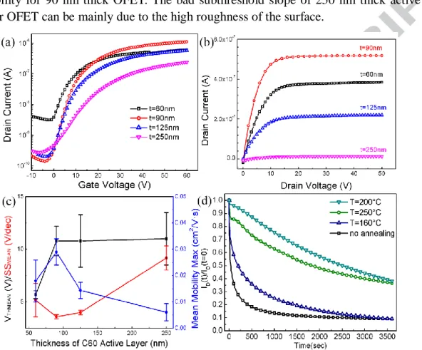
3.3 Effect of the thickness of the C60 active layer on the OFET annealed at 200°C
Another experimental parameter that can influence the properties of the OFETs is the thickness of the C60 active layer. Following the previous study, the effect of this
thickness on the properties of the OFETs, annealed at 200°C after their fabrication, is presented hereafter.
Fig. 6 shows the mean transfer and output characteristics of 4 OFETs having a C60 active layer with a thickness of 60nm, 90 nm, 125 nm or 250nm. All the OFETS
µm. The best characteristics are obtained for an active layer of 90 nm thick. The behavior of the electrical parameters as a function of the thickness is shown also in Fig. 6c and their values are presented in Table 3. It seems that the low performance of the 60 nm thick active layer OFETs is probably due to low coverage between the active layer and the 205 nm thick source and drain contacts. The performance of 90 nm thick and 125 nm thick active layer OFETs are more or less similar with higher mobility for 90 nm thick OFET. The bad subthreshold slope of 250 nm thick active layer OFET can be mainly due to the high roughness of the surface.
Fig. 6: (a), (b), (c): Mean transfer and output characteristics of several OFETs having the same size (channel width W=4000 µm, channel length L=150 µm) and a C60 active layer with a thickness of
60nm, 90 nm, 125 nm or 250nm. The behavior of their mean electrical parameters (Threshold voltage, subthreshold slope and mobility) is also reported. (d) Drain-current of OFETs using 90 nm thick C60 active layer un-annealed and annealed at different temperatures, 160°C, 200°C, 250°C as a function of
the time under 40V gate-source voltage and 20V drain-source voltage Table 3
Main mean electrical parameters of several OFETs having the same size (channel width W=4000 µm, channel length L=150 µm) and a C60 active layer with a thickness tC60 of 60nm, 90 nm, 125 nm or
250nm, all annealed at 200°C. VTH is the threshold voltage, SS the subthreshold slope, µ the field effect
mobility, RC the contact resistance, µ after RC the mobility after correction by RC, Ioff is the minimum
current and Ion/Ioff is the ratio between the maximum current and the minimum current.
tC60 (nm) VTH (V) SS (V/dec) µ (cm2/V.s) Rc () µ after Rc (cm2/V.s) Ioff (A) Ion/Ioff 60 5,7 5,2 1.8x10⁻² 2.7x10⁶ 1.9x10⁻² 3x10⁻⁹ 180
90 10,8 3,6 2.9x10⁻² 7.5x10⁵ 2.95x10⁻² 1.4x10⁻¹⁰ 7.8x10³
125 10,8 4 1.4x10⁻² 1.2x10⁷ 1.7x10⁻² 2x10⁻¹⁰ 2.85x10³
250 11 9,2 6.1x10⁻³ 1x10⁷ 6.5x10⁻³ 2.7x10⁻¹⁰ 870
In conclusion, the best conditions to prepare the evaporated C60 active layer of
printed bottom-gate/bottom-contacts OFETs, are obtained with a thickness of 90 nm and a post-thermal annealing equal 200°C.
To re-inforce this conclusion, the drain-current of OFETs using 90 nm thick C60
active layer and annealed at different temperatures, was plotted as a function of the time when constant gate voltage VGS and drain voltage VDS are applied. Under
VGS=40V and VDS=20V, the drain current decreases with the time (Fig. 6d). In these
conditions, the 200°C annealed OFETs have the slowest decrease leading to more reliable value of the current under constant biasing.
3.4 Dynamic behavior of the optimized printed C60 based OFET
Defining then the best conditions to prepare the evaporated C60 active layer of
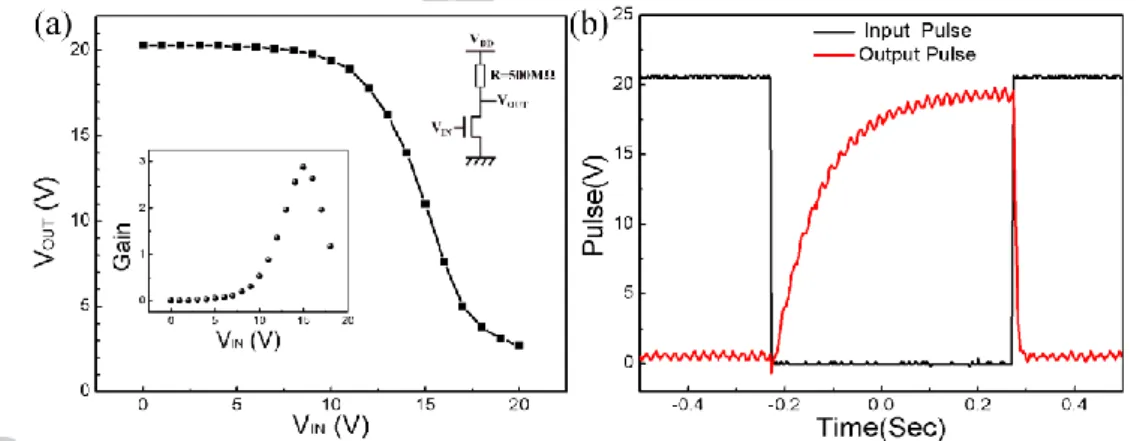
printed bottom-gate/bottom-contacts OFETs and knowing their static performances, is a prerequisite step to evaluate their optimum dynamic performance. The dynamic performance is studied through the behavior of resistive loaded OFET under square pulsed voltage applied to its gate.
Static output characteristic of the OFET as an inverter is presented in Fig.7. The load resistance R is fixed to 500M and the circuit is biased by VDD=20V.
Fig. 7: (a) Static output characteristic of printed C60 based OFET loaded by 500MΩ resistance and
(b) its response to 1Hz pulse. The inset shows the gain of the inverter with a maximum value of 3.
In these polarization conditions, the inverter has a gain (maximum of the differentiation dVOUT/dVIN) of 3 (Fig.7a). This value depends on the load resistance of
course. But, it is in the order of the gain of organic based OFETs inverters [21]. The minimum output voltage VOL with the maximum input voltage VIN is explained by the
resistance value of the channel in on-state compared to the load resistance.
More interestingly than the static characteristic, the dynamic response of the OFET to a voltage pulse gives a better idea of its performance. When applying 20V pulse of 0.5 second duration (1 Hz frequency) to the gate of the OFET, the behavior of the output voltage gives its time response (as shown in fig.7b). When the gate-source voltage switches from 20V to 0V, the OFET status switches from the on-state to the off-state and then the output voltage has to switch from nearly 0V to nearly 20V. The
switch time is defined usually by the time from 10% to 90% of the maximum voltage. In the case of the present OFET, the switching time is 220 ms. This time is due to the load resistance as its value is much lower than the resistance of the channel in off-regime, 500M compared to some hundreds G.
The more significant time is the switching time between the off-state and the on-state that depends nearly only on the transistor. This time corresponds to the decrease of the output voltage from the maximum to the minimum value. The switching time from 90% to 10% of the maximum voltage is 13 ms here. Present OFET can answer to more than 10Hz frequency. However, the frequency can be increased more by optimizing the overlap between the gate contacts and source and drain contacts and by chemically modifying the surface of drain and source electrodes before the deposition of C60 active layer as we have done previously for photolithography processed C60 OFETs where 1.5 cm2/V.s was obtained [22]. In fact, the frequency can be considered depending on the applications. For example, 100Hz frequency is enough if OFETs are integrated into a treatment electronic circuit of signals coming from human body activities. Such 100Hz frequency can be reached with such process improvement.
4 Conclusion
The main purpose of present work was devoted to the optimization of the last deposited layer in bottom-gate bottom contacts printed C60 based OFET. This last
deposited layer is a film of C60.The first steps of the process were the printing of the
silver gate contact, the photoresist SU8 gate insulator, the drain and source silver contacts. All these steps were previously optimized and the results were published in different papers [10,11]
The effect of the post-annealing temperature of the fabricated OFET was studied firstly. Direct correlation between the structure of the C60 film (grain size, surface
roughness) as analyzed from AFM observation and electrical parameters of the OFET was highlighted. More than the correlation, proportionality between the grain size and the field effect mobility was evidenced. The surface roughness is effective only when the grain size does not change a lot. The proportionality between the grain size and the mobility led us to involve the usual Seto model [17] and its derivatives established for polycrystalline films and thin film transistors based on. Treatment of the experimental curves fit well with this model leading us to the calculation of the defect density in the grain boundaries. In our knowledge, such detailed analysis was never made before on the effect of the post-annealing temperature on organic transistors. Determining the 200°C optimum post-annealing temperature, the thickness of the C60
active layer was optimized at 90 nm and confirmed by electrical stability study of the drain current during continuous polarization of the transistor. Considering the potential main application of such transistors in electronic circuits for the treatment of analog signals coming from the human body activities, the response of present OFETs to a voltage pulse applied to the gate was measured. A switching time of 13 ms was obtained, leading to application frequency of some 10Hz.
chemical modification of the surface of the contacts will be done soon in the goal to improve the stability and to increase the working frequency. The use of active charge (another NMOS OFET) in pseudo-CMOS inverter will be integrated soon in the purpose to get symmetric answer to a voltage pulse (similar rise time and fall time) will be done very soon. Finally, the integration of printed pentacene based P-type OFET is planned to reach the final goal of CMOS electronics.
References:
[1] Hayward J., Chansin, Zervos H., Wearable Technology 2017-2027: Markets, Players, Forecasts, IDTechEx report, 2017.
[2] Kobayashi S, Takenobu T, Mori S, Fujiwara A, Iwasa Y. Fabrication and characterization of C 60 thin-film transistors with high field-effect mobility. Applied physics letters. 2003;82:4581-3.
[3] Anthopoulos TD, Singh B, Marjanovic N, Sariciftci NS, Montaigne Ramil A, Sitter H, Colle M & de Leeue DM. High performance n-channel organic field-effect transistors and ring oscillators based on C 60 fullerene films. Applied Physics Letters. 2006;89:213504.
[4] Zhang X-H, Domercq B, Kippelen B. High-performance and electrically stable C 60 organic field-effect transistors. Applied Physics Letters. 2007;91:092114.
[5] Singh M, Haverinen HM, Dhagat P, Jabbour GE. Inkjet printing—process and its applications. Advanced materials. 2010;22:673-85.
[6] Romain M, Chevrier M, Bebiche S, Mohammed-Brahim T, Rault-Berthelot J, Jacques E & Poriel C. The structure–property relationship study of electron-deficient dihydroindeno [2, 1-b] fluorene derivatives for n-type organic field effect transistors. Journal of Materials Chemistry C. 2015;3:5742-53.
[7] Sirringhaus H, Kawase T, Friend R, Shimoda T, Inbasekaran M, Wu W & Woo EP. High-resolution inkjet printing of all-polymer transistor circuits. Science. 2000;290:2123-6.
[8] Calvert P. Inkjet printing for materials and devices. Chemistry of materials. 2001;13:3299-305.
[9] de Gans BJ, Duineveld PC, Schubert US. Inkjet printing of polymers: state of the art and future developments. Advanced materials. 2004;16:203-13.
[10] Robin M, Kuai W, Amela-Cortes M, Cordier Sp, Molard Y, Mohammed-Brahim T, Jacques E & Harnois M. Epoxy based ink as versatile material for inkjet-printed devices. ACS applied materials & interfaces. 2015;7:21975-84.
[11] Moon SJ, Robin M, Wenlin K, Yann M, Bae BS, Mohammed-Brahim T, Jacques E & Harnois M. Morphological impact of insulator on inkjet-printed transistor. Flexible and Printed Electronics. 2017;2:035008.
[12] Le Borgne B, De Sagazan O, Crand S, Jacques E, Harnois M. Conformal Electronics Wrapped Around Daily Life Objects Using an Original Method: Water Transfer Printing. ACS applied materials & interfaces. 2017;9:29424-9.
[13] Senthilkumar M, Sahoo N, Thakur S, Tokas R. Characterization of microroughness parameters in gadolinium oxide thin films: A study based on extended power spectral density analyses. Applied surface science. 2005;252:1608-19.
[14] Rolland A, Richard J, Kleider J, Mencaraglia D. Electrical properties of amorphous silicon transistors and MIS‐ devices: comparative study of top nitride and bottom nitride configurations. Journal of the electrochemical society. 1993;140:3679-83.
[15] Levinson J, Shepherd F, Scanlon P, Westwood W, Este G, Rider M. Conductivity behavior in polycrystalline semiconductor thin film transistors. Journal of Applied Physics. 1982;53:1193-202.
[16] Bonnaud O, Mohammed-Brahim T, Ast DG. Poly-Si Thin Film and Substrate Materials. Thin Film Transistors: Polycrystalline Silicon Thin Film Transistors Bd. 2004;2:8-94.
[17] Seto JY. The electrical properties of polycrystalline silicon films. Journal of Applied Physics. 1975;46:5247-54.
[18] Bebiche S. OTFTs de type N à base de semiconducteurs π-conjugués: fabrication, performance et stabilité: Rennes 1; 2015.
[19] Chern G, Mathias H, Testardi L, Seger L, Schlenoff J. Low-frequency dielectric permittivity of C 60. Journal of superconductivity. 1995;8:207-10.
[20] Mourgues K, Rahal A, Mohammed-Brahim T, Sarret M, Kleider J, Longeaud C, Bachrouri A & Romano-Rodriguez A. Density of states in the channel material of low temperature polycrystalline silicon thin film transistors. Journal of Non-Crystalline Solids. 2000;266:1279-83.
[21] Chang JS, Facchetti AF, Reuss R. A Circuits and Systems Perspective of Organic/Printed Electronics: Review, Challenges, and Contemporary and Emerging Design Approaches. IEEE Journal on Emerging and Selected Topics in Circuits and Systems. 2017;7:7-26.
[22] Robin M, Harnois M, Molard Y, Jacques E. Improvement of n-type OTFT electrical stability by gold electrode modification. Organic Electronics. 2016;39:214-21.
Figure Captions
Fig. 1: Cross-section of the C60 OFETs using bottom gate and bottom contacts geometry. The figure highlights the problematic of the high aspect ratio between the drain and source contacts and the gate insulator
Fig. 2: Fabrication process of C60 OFET
Fig. 3: 2D ( ) AFM images, corresponding 3D enlarged ( ) (a) as-deposited; and after annealing at 160Cº (b), 200°C (c) and 250°C (d)
Fig. 4: (a)Mean transfer characteristics (VD=20V) and (b) output characteristics (VG=20V) of several
OFETs having the same size (channel width W=4000 µm, channel length L=150 µm) and 125 nm thick C60 active layer, measured as-fabricated and after annealing at 160°C, 200°C and 250°C.
Fig. 5: (a) Behavior of the mean threshold voltage VTHMEAN , subthreshold slope SSMEAN and field
effect mobility, when the annealing temperature increases; (b) Similar behavior of the mobility and the grain size as a function of the annealing temperature; (c) Behavior of the subthreshold slope SS, the surface roughness and the grain size as a function of the annealing temperature; (d) Semi-logarithmic plot of ID/(VG-Vmin) versus 1/(VG-Vmin) for OFETs annealed at 160°C and 200°C
Fig. 6: (a), (b), (c): Mean transfer and output characteristics of several OFETs having the same size (channel width W=4000 µm, channel length L=150 µm) and a C60 active layer with a thickness of
60nm, 90 nm, 125 nm or 250nm. The behavior of their mean electrical parameters (Threshold voltage, subthreshold slope and mobility) is also reported. (d) Drain-current of OFETs using 90 nm thick C60 active layer un-annealed and annealed at different temperatures, 160°C, 200°C, 250°C as a function of the time under 40V gate-source voltage and 20V drain-source voltage
Fig. 7: (a) Static output characteristic of printed C60 based OFET loaded by 500MΩ resistance and (b)
its response to 1Hz pulse. The inset shows the gain of the inverter with a maximum value of 3.
Table Captions
Table 1: RMS roughness and grain size calculated using PSDF formulation (1)
Table 2: Main mean electrical parameters of several OFETs having the same size (channel width W=4000 µm, channel length L=150 µm) and 125 nm thick C60 active layer, measured as-fabricated and
after annealing at TA=160°C, 200°C and 250°C. VTH is the threshold voltage, SS the subthreshold slope,
µ the field effect mobility, RC the contact resistance, µ after RC the mobility after correction by RC, Ioff
is the minimum current and Ion/Ioff is the ratio between the maximum current and the minimum current
Table 3: Main mean electrical parameters of several OFETs having the same size (channel width W=4000 µm, channel length L=150 µm) and a C60 active layer with a thickness tC60 of 60nm, 90 nm,
125 nm or 250nm, all annealed at 200°C. VTH is the threshold voltage, SS the subthreshold slope, µ the
field effect mobility, RC the contact resistance, µ after RC the mobility after correction by RC, Ioff is the
Investigation of thermal annealing process influence on printed n-type OFET Investigation of organic semiconductor layer thickness impacts on C60 OFET Investigation on relationships between OFET stability and C60 crystalline structure Investigation on Pseudo-CMOS inverter logic circuits