Titre:
Title
: Tunable diplexer for cognitive radio RF front-end modules
Auteurs:
Authors
: Erick Emmanuel Djoumessi et Ke Wu
Date: 2014
Type:
Article de revue / Journal articleRéférence:
Citation
:
Djoumessi, E. E. & Wu, K. (2014). Tunable diplexer for cognitive radio RF front-end modules. Universal Journal of Electrical and Electronic Engineering, 2(7), p. 278-285. doi:10.13189/ujeee.2014.020703
Document en libre accès dans PolyPublie
Open Access document in PolyPublieURL de PolyPublie:
PolyPublie URL: https://publications.polymtl.ca/4854/
Version: Version officielle de l'éditeur / Published versionRévisé par les pairs / Refereed Conditions d’utilisation:
Terms of Use: CC BY
Document publié chez l’éditeur officiel
Document issued by the official publisherTitre de la revue:
Journal Title: Universal Journal of Electrical and Electronic Engineering (vol. 2, no 7)
Maison d’édition:
Publisher: Horizon Research Publishing
URL officiel:
Official URL: https://doi.org/10.13189/ujeee.2014.020703
Mention légale:
Legal notice:
Ce fichier a été téléchargé à partir de PolyPublie, le dépôt institutionnel de Polytechnique Montréal
This file has been downloaded from PolyPublie, the institutional repository of Polytechnique Montréal
Tunable Diplexer for Cognitive Radio RF
Front-end Modules
Erick Emmanuel Djoumessi
1,*, Ke Wu
21Intel Corporation, Libertyville, 60048, Illinois, United States
2Poly-Grames Research Center, Ecole Polytechnique de Montreal, Montreal, H3T1J4, Quebec, Canada
*Corresponding Author: [email protected]
Copyright © 2014 Horizon Research Publishing. All rights reserved.
Abstract
This paper describes the design andmeasurement of a varactor-tuned planar diplexer for reconfigurable multi-mode/multi-standard transceiver front-end modules. The proposed diplexer of 3 cm × 1.8 cm is composed of two tunable dual-mode bandpass filters with two varactor diodes. The diplexer channels are 8.8% relative bandwidth at 2.48 and 3.2 GHz for 25 V biased voltage, while 7.5% and 4.1% are obtained at 2.075 and 2.606 GHz for 5 V, respectively. The center-frequency tunability for lower and upper channel filters bands are 21.4% and 20.4%, respectively. Measured insertion loss varies from 2.4 to 4.8 dB and 2.8 to 5 dB for the two channels over the tuning frequency range with better than 30-dB isolation. The lower channel filter (with higher capacitance) presents a better 1-dB compression measurement point (P-1dB) over the tuning frequency range.
Keywords
Tunable Diplexer, Dual-Mode Filter,Tunable Transceiver, Varactor Diode, Cognitive Radio, SDR
1. Introduction
Bluetooth, IEEE802.16 and IEEE802.11a/b/g wireless radio technologies for personal area networks (PAN), wireless metropolitan area networks (WMAN) and wireless local area networks (WLAN), have been developed to meet different cellular phone service requirement. Thus, wireless platforms are equipped with more and more radio transceivers operating in parallel on chips to satisfy those needs. However, the power consumption, cost and interference between radios chipsets are major problems encountered by those systems. An emerging solution is related to the development of reconfigurable microwave components to realize radio systems that can dynamically detect available channel access in order to improve overall spectrum usage. In [1], a Ka-band ferroelectric thin film/dielectric diplexer was realized as a critical part of a
discriminator–locked tunable oscillator. Moreover, tunable RF front-end components that have largely been studied and implemented for the future software defined cognitive radio systems (SDCR) are RF filters [2], [3], couplers [4], [5] ], and demodulators [6]. In this letter, a varactor-tuned planar dual-mode bandpass filter is used to design a tunable diplexer. Simulations and measurements results of S-parameters and 1-dB compression point for different biased voltage are also presented.
2. Varactor-Tuned Dual-Mode
Bandpass Filter
Fig. 1(a) shows the structure of the proposed tunable diplexer. It consists of two capacitively loaded second-order microstrip dual-mode bandpass filters (BPF) and a tee junction connecting the individual BPFs to a common input port 1. Let the upper and lower filters be named filter 1 and filter 2, respectively. The microstrip dual-mode resonator is widely used to design bandpass filters due to its compact size and selectivity. A tunable dual-mode bandpass filter was presented in [3]. However, very little effort has been focused on its detailed analysis. For our analysis purpose, such a square microstrip dual-mode resonator can be represented as a resonant cavity with TMz
mn0 modes. The analytical
expressions of EM fields within the cavity have well been detailed in [7]. According to the boundary conditions, the analytical expressions of electric and magnetic fields within the cavity are given by Eq. (1), where indexes m, n characterize modes and kc, ω are respectively the propagation constant and the angular frequency. Amn and εeff stand for mode magnitude and dielectric effective permittivity. 0 0 cos cos z mn m n m m E A x y a a π π ∞ ∞ = = =
∑ ∑
2 eff z x c j E H k y ωε ∂ = ∂ (1) 2 eff z y c j E H k x ωε ∂ = − ∂ Universal Journal of Electrical and Electronic Engineering 2(7): 278-285, 2014 279
(a)
(b)
Figure 1. (a) Layout of the proposed tunable diplexer based-on two
identical two-pole dual-mode bandpass filter loaded with two different capacitances, (b) equivalent circuit of a dual-mode bandpass filter
The first resonant degenerated modes TM100 and TM010 within the cavity are characterized by the frequency given as fc= 2/ λg (μεeff)1/2, where λg is the guided wavelength evaluated at the center operation frequency, and εeff stands for dielectric effective permittivity. To illustrate and facilitate the design principle of the tunable diplexer, Fig. 1(b) presents a circuit model of the two pole dual-mode BPF (as shown in Fig. 1(a)). Both degenerated modes are represented by L1,2C1,2, series resonators, magnetically coupled through coupling coefficient M12, used to model the perturbation pxp in combination with capacitor Cp1,2. Cross-coupling capacitor C3 models the direct coupling between the input and output (I/O) ports (as shown in Fig 1(a) by variable d) and it is used to create a pair of transmission zeros for improving the dual-mode filter selectivity. The external quality factor Qext1= Qext2 [8] can be found from coupling gap s1 and line width w1.
To validate the proposed circuit model, the tunable filter 1 is designed at f1= 3.2 GHz by using EM software ADS Momentum [9]. The substrate used is Rogers RT/Duroid 6010 with thickness of 0.635 mm and relative permittivity εr= 10.2. Geometrical dimensions are wp = 0.593 mm, w1 = 0.1523 mm, w = 0.3 mm, l1 = 2.43 mm, l2 = 1.3 mm, l3 = 1.2 mm, l4 = 1.7 mm, l5 = 3.5 mm, s1 = 0.1524 mm, wn= 0.15 mm, ln= 3.2 mm and Cvar1= Cp1= 0.45 pF. Circuit model [see Fig. 1(b)] parameters values are given as: Lin= Lout= 12.4 nH, Cin= Cout= 0.22pF, L1= L2= 10 nH, C1= C2= 0.25 pF, M12= 0.04, C3= 0.1pF. Analytical expressions of the external/unloaded quality factors (Qext, Qu) [4], and
coupling coefficients K12 are given by:
(2)
where f01 and f02 represent the two resonant frequencies modes TM100 and TM010. f0, f2-f1 and IL (insertion loss) are for the center operation frequency, 3-dB bandwidth and insertion loss in dB, respectively. Fig. 2 shows the computed values of Q and K12 against gap s1 and for different values of Cvar1 and Cp1. As the loaded capacitances Cvar1= Cp1= Cvar increase with a constant value of s1, the external Qext increases (i.e: 3-dB bandwidth decreases and Qu increases) (see Fig. 2(a)). However, the insertion loss increases with the loaded Cvar, as a consequence of mismatch. Maximum values of Qu= 96, 110, 117 are obtained at different s1= 0.05, 0.16, 0.26 mm for various Cvar= 0.45, 0.65 and 0.85 pF, respectively. Fig. 2(a) shows that Q-factor at different Cvar, can be controlled by simply tuning gap s1. On the other hand, ratio f02/f01 and coefficient K12 against capacitance Cp1 are shown in Fig. 2(b) for different values of Cvar1= 0.45 and 0.65 pF, respectively. To keep a constant K12= M12= 0.04 (3-dB bandwidth) at different center-operation frequency defined by Cvar= 0.45 and 0.85 pF, the value of Cp1 should be 0.425 to 0.92 pF (see Fig. 2(b)).
(a)
(b)
Figure 2. (a) External and unloaded quality factor, (b) two degenerate mode
frequencies and their coupling coefficients for different values of loading capacitances Cvar and Cp.
via Cp2 C var2 Cvar2 Cvar2 Cvar2 wn Ln l1 l4 l2 s1 l3 pxp wp D<λg/4 w 1 2 3 l1 l4 l4 l l2 l2 l s1 l3 px px p pxpx wp wp w w 2 via Cp Cp C2 C var Cvar C 2 Cvar Cvar C 2 Cvar Cvar C 2 Cvar Cvar C 2 wn Ln 3 Channel filter 1 Channel filter 2
w1 l5 l6 y x z Cp1 Cvar1 Cvar1 l7 d d C1 C2 Input port C1 C1 C Mode 1 C2 C2 C Mode 2 M12 C3 Qext1 Cin Lin L1/2 L1/2 Outputport Qext2 Cout Lout L2/2 L2/2 2 2 02 01 12 2 2 02 01 f f k f f − = + 0 2 1 ext
f
Q
f
f
=
−
/20(1 10
ext)
u ILQ
Q
=
−−
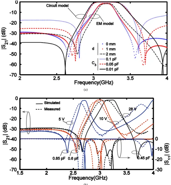
Typical simulated responses of the circuit and (EM) model as shown in Fig. 3(a). Both models show responses with a pair of transmission zeros at the edge of the filter bandpass for various values of C3 (0.01, 0.05, 0.1 pF) and d (0, 1, 2 mm) to demonstrate the influence of the transmission zeros on the insertion loss. When the value of C3 increases (d decreases), the upper and lower stopband transmission zeros will be closer to the passband edges with the stable passband insertion loss that is essentially not degraded. The circuit model shows a broadband frequency response than the EM model. This is mainly due to the ideal lossless lumped elements used in the circuit model that result to an IL=0. Eq. (2) also shows that as IL increase, the 3-dB bandwidth decrease (see Fig. 3(a)).
Finally, capacitances Cvar1 and Cp1 are replaced by identical varactor diodes, denoted by C. The chip varactor diode used is the MSV34,069 from Aeroflex Metelics, with capacitance variation from 0.4 to 2.5 pF over a 30-V bias voltage with equivalent resistance of 0.8 Ω. As shown in Fig. 3(b), simulated and measured results (S21 and S11) at different bias voltage are in good agreement. The measured insertion losses at the center operation frequency vary from 2.2 to 5.2 dB with 20.7% ((fmax-fmin)/(fmax+fmin)/2) center-frequency tunable range from approximately 2.6 to 3.2 GHz. The frequency shift observed between the simulation and measurement results are mainly due to the wire bonding effect used to connect the varactor diode to the microstrip line.
(a)
(b)
Figure 3. (a) Circuit model and EM simulated frequency responses of a dual-mode BPF for various values of C3 and d with M12= 0.04 and Cp= Cvar= 0.45pF,
Universal Journal of Electrical and Electronic Engineering 2(7): 278-285, 2014 281
3. Electronically Tunable Diplexer
A tunable dual-mode BPF has been designed and experimentally validated for the diplexer upper channel band by using a varactor diode MSV34069. The same procedure is used to design the lower channel filter 2 with the center frequency at f2= 2.6 GHz. A varactor diode MSV34075, with capacitance variation from 0.7 to 4 pF over a 30-V bias voltage with equivalent resistance of 0.5 Ω, is used to reduce the filter size and thus the same bias voltage supply (Vb) as for the upper channel filter 1 is also preserved. Geometrical dimensions of tunable BPF 2 are the same as for the filter 1, except length l4= 2.4 mm and capacitance Cvar2= Cp2= 0.8 pF. Connection of both tunable BPF 1 and 2 to the common input port 1 is realized by T-junction with physical lengths l6= 6 mm and l7= 7.7 mm. Fig. 4 shows the fabricated tunable diplexer prototype. Simulation and measurement S-parameters are shown in Figs. 5 for different capacitances Cvar1,2 and biased voltage Vb. Bias voltage range Vb, corresponding to the tuning capacitance range (from 0.45 to 0.85 pF for MSV34069 and from 0.8 to 1.2 pF for MSV34075), covers about 25 to 5 volt. The tunable upper and lower channel filters exhibit 20.4% and 21.4% tunable range from approximately 2.606 to 3.2 GHz, and 2.075 to 2.48 GHz. The measured 3-dB bandwidth in the tuning range is around 8.8% at 2.48 and 3.2 GHz for 25 V biased voltage, while 7.5% and 4.1% are obtained at 2.075 and 2.606 GHz for 5 V, respectively. The measured insertion loss losses (S31 and S21) vary from 2.4 to 4.8 dB and 2.8 to 5 dB for the two channels over the tuning frequency range with better than 30-dB isolation (S23). Such insertion losses are mainly due to the combination of substrate dielectric loss and
silicon varactor diode loss that increases as the bias voltage decreases (capacitance increases). The measured return loss (S11, S22, and S33) at the common port 1, output port 2 and 3 are from -7 to -20 dB in the upper and lower passbands.
Figure 4. Photograph of fabricated tunable diplexer
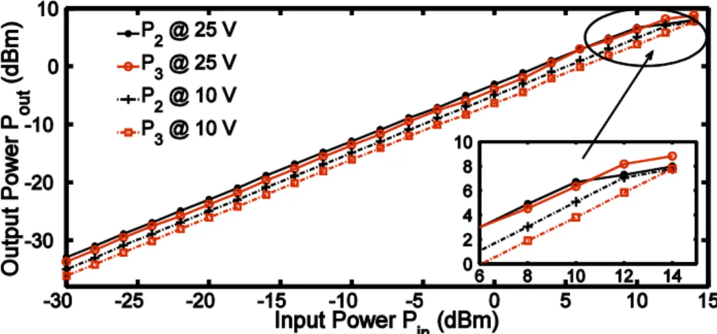
Since varactor diodes MSV34069 and MSV34075 present nonlinear characteristics, a RF input signal tone (Pin) level is applied at common port 1 of the diplexer and the output signal (Pout) level is measured at ports 2 and 3. Fig. 6 shows the measured Pout versus Pin for bias voltage Vb= 25 and 10 volt, corresponding to the lower/upper center-operation frequency of 2.2/2.8 GHz and 2.51/3 GHz, respectively. As shown in Fig. 6, the Pout signal level saturation suggests a better 1-dB compression point (as well as linearity) and insertion loss for the lower channel BPF 2 (loaded with diode MSV34075), than its upper counterpart with varactor MSV34069. These results suggest the usefulness of BPF 2 and BPF 1 as transmit and receive channel pasbands, respectively. (a) (RX) Channel filter 1 2 3 1 (TX) Channel filter 2 Varactor Varactor
(b)
(c)
(d)
Figure 5. Simulated and measured results of magnitudes of S11, S21, S31, S22, S33 and S23 for ((a), (b)) Cvar1= Cp1= 0.45 pF, Cvar2= Cp2= 0.8 pF, Vb= 25 v, and
Universal Journal of Electrical and Electronic Engineering 2(7): 278-285, 2014 283
Figure 6. Output power level Pout at ports 2 and 3 against input power level Pin at port 1, for different biased voltage Vb= 10, 25 v.
3. Conclusion
A frequency-agile diplexer is proposed and experimentally validated by using tunable dual-mode bandpass filters. The diplexer compact size of 3 cm × 1.8 cm is achieved with two types of silicon varactor diode. Both adjacent channel center-frequency tunabilities are 21.4% and 20.4% with isolation better than 30 dB. The proposed diplexer can be used for tunable multi-mode/multi-standard transceiver systems.
Acknowledgements
The authors thank the technical personal of Poly-Grames Research Center, Ecole Polytechnique de Montreal, in the fabrication and mounting of the diplexer prototype.
REFERENCES
[1] F., A. Miranda, G. Subramanvam, K. Van, F. W. Romanofsky, “A K-band (HTS gold)/ferroelectric thin film/dielectric
diplexer for a discriminator locked tunable oscillator,” IEEE Trans. Applied Supercon., vol. 9, no. 2, pp. 3581-3584, June 1999.
[2] M. A. El-Tanani, and G. M. Rebeiz, “A two-pole two-zero tunable filter with improved linearity,” IEEE Trans. Microw. Theory Tech., vol. 57, no. 4, pp. 830-840, April. 2009. [3] E. E. Djoumessi, M. Chaker, and K. Wu, “Varactor-tuned
dual-mode bandpass filter for wireless applications, ” in Radio Wireless Conf., Jan. 2009, pp. 646-649.
[4] M., H., Lehmann, T., Knoechel, “Systematic design of reconfigurable quadrature directional couplers,” IEEE MTT-S, pp. 1009-1012, June. 2009.
[5] E. E. Djoumessi, and K. Wu, “Varactor-tuned multiband six-port front-end for wireless applications,” Asia-Pacific Conf., pp. 1-5, Dec. 2008.
[6] E. E. Djoumessi, and K. Wu, “Tunable multi-band direct conversion receiver for cognitive radio systems,” IEEE MTT-S, pp. 217-220, Jun. 2009.
[7] J.S Hong, M. J. Lancaster, Microstrip Filters for RF/Microwave Applications, New York: Wiley, 2001. [8] K. Chang, L. H. Hsieh, Microwave Ring Circuits and Related
Structures: New York: Wiley, 2004.