HAL Id: tel-01848782
https://tel.archives-ouvertes.fr/tel-01848782
Submitted on 25 Jul 2018HAL is a multi-disciplinary open access archive for the deposit and dissemination of sci-entific research documents, whether they are pub-lished or not. The documents may come from teaching and research institutions in France or
L’archive ouverte pluridisciplinaire HAL, est destinée au dépôt et à la diffusion de documents scientifiques de niveau recherche, publiés ou non, émanant des établissements d’enseignement et de recherche français ou étrangers, des laboratoires
Development of novel organic optoelectronic
technologies for biomedical applications
Shahab Rezaei Mazinani
To cite this version:
Shahab Rezaei Mazinani. Development of novel organic optoelectronic technologies for biomedical applications. Other. Université de Lyon, 2017. English. �NNT : 2017LYSEM028�. �tel-01848782�
THESE de DOCTORAT DE L’UNIVERSITE DE LYON
opérée au sein de
l’Ecole des Mines de Saint-Etienne
Ecole Doctorale N° 488Sciences, Ingénierie, Santé
Spécialité de doctorat : Microélectronique Discipline : Bioélectronique Organique
Soutenue publiquement le 16/10/2017, par : Shahab REZAEI MAZINANI
Development of Novel Organic Optoelectronic
Technologies for Biomedical Applications
Devant le jury composé de :
Président : Christophe Bernard Directeur de recherche 1, INSERM,
Aix-Marseille Université
Rapporteurs : John de Mello Professor, Imperial College London
Alexander Fleischmann Chargé de recherche 1, INSERM, Collège de France
Examinateurs : Andreas Offenhäusser Professor, Forschungszentrum Jülich, Helmholtz-Gemeinschaft
Paschalis Gkoupidenis Group leader, Max Planck Institute for Polymer Research
Directeur de thèse : George Malliaras Professor,
Ecole des Mines de Saint-Etienne
Co-encadrante : Esma Ismailova Associate Professor,
ABSI Nabil CR Génie industriel CMP AUGUSTO Vincent CR Image, Vision, Signal CIS AVRIL Stéphane PR2 Mécanique et ingénierie CIS BADEL Pierre MA(MDC) Mécanique et ingénierie CIS
BALBO Flavien PR2 Informatique FAYOL
BASSEREAU Jean-François PR Sciences et génie des matériaux SMS BATTON-HUBERT Mireille PR2 Sciences et génie de l'environnement FAYOL
BEIGBEDER Michel MA(MDC) Informatique FAYOL BLAYAC Sylvain MA(MDC) Microélectronique CMP
BOISSIER Olivier PR1 Informatique FAYOL
BONNEFOY Olivier MA(MDC) Génie des Procédés SPIN BORBELY Andras MR(DR2) Sciences et génie des matériaux SMS BOUCHER Xavier PR2 Génie Industriel FAYOL BRODHAG Christian DR Sciences et génie de l'environnement FAYOL BRUCHON Julien MA(MDC) Mécanique et ingénierie SMS CAMEIRAO Ana MA(MDC) Génie des Procédés SPIN CHRISTIEN Frédéric PR Science et génie des matériaux SMS DAUZERE-PERES Stéphane PR1 Génie Industriel CMP DEBAYLE Johan MR Sciences des Images et des Formes SPIN DEGEORGE Jean-Michel MA(MDC) Génie industriel Fayol DELAFOSSE David PR0 Sciences et génie des matériaux SMS DELORME Xavier MA(MDC) Génie industriel FAYOL DESRAYAUD Christophe PR1 Mécanique et ingénierie SMS
DJENIZIAN Thierry PR Science et génie des matériaux CMP DOUCE Sandrine PR2 Sciences de gestion FAYOL DRAPIER Sylvain PR1 Mécanique et ingénierie SMS FAUCHEU Jenny MA(MDC) Sciences et génie des matériaux SMS FAVERGEON Loïc CR Génie des Procédés SPIN FEILLET Dominique PR1 Génie Industriel CMP FOREST Valérie MA(MDC) Génie des Procédés CIS FRACZKIEWICZ Anna DR Sciences et génie des matériaux SMS GARCIA Daniel MR(DR2) Sciences de la Terre SPIN GAVET Yann MA(MDC) Sciences des Images et des Formes SPIN GERINGER Jean MA(MDC) Sciences et génie des matériaux CIS GOEURIOT Dominique DR Sciences et génie des matériaux SMS GONDRAN Natacha MA(MDC) Sciences et génie de l'environnement FAYOL GONZALEZ FELIU Jesus MA(MDC) Sciences économiques FAYOL GRAILLOT Didier DR Sciences et génie de l'environnement SPIN GROSSEAU Philippe DR Génie des Procédés SPIN GRUY Frédéric PR1 Génie des Procédés SPIN GUY Bernard DR Sciences de la Terre SPIN HAN Woo-Suck MR Mécanique et ingénierie SMS HERRI Jean Michel PR1 Génie des Procédés SPIN KERMOUCHE Guillaume PR2 Mécanique et Ingénierie SMS KLOCKER Helmut DR Sciences et génie des matériaux SMS LAFOREST Valérie MR(DR2) Sciences et génie de l'environnement FAYOL
LERICHE Rodolphe CR Mécanique et ingénierie FAYOL MALLIARAS Georges PR1 Microélectronique CMP MOLIMARD Jérôme PR2 Mécanique et ingénierie CIS MOUTTE Jacques CR Génie des Procédés SPIN
NEUBERT Gilles FAYOL
NIKOLOVSKI Jean-Pierre Ingénieur de recherche Mécanique et ingénierie CMP NORTIER Patrice PR1 Génie des Procédés SPIN O CONNOR Rodney Philip MA(MDC) Microélectronique CMP OWENS Rosin MA(MDC) Microélectronique CMP PERES Véronique MR Génie des Procédés SPIN PICARD Gauthier MA(MDC) Informatique FAYOL PIJOLAT Christophe PR0 Génie des Procédés SPIN
PINOLI Jean Charles PR0 Sciences des Images et des Formes SPIN POURCHEZ Jérémy MR Génie des Procédés CIS
ROUSSY Agnès MA(MDC) Microélectronique CMP ROUSTANT Olivier MA(MDC) Mathématiques appliquées FAYOL
SANAUR Sébastien MA(MDC) Microélectronique CMP STOLARZ Jacques CR Sciences et génie des matériaux SMS TRIA Assia Ingénieur de recherche Microélectronique CMP VALDIVIESO François PR2 Sciences et génie des matériaux SMS VIRICELLE Jean Paul DR Génie des Procédés SPIN WOLSKI Krzystof DR Sciences et génie des matériaux SMS
EMSE : Enseignants-chercheurs et chercheurs autorisés à diriger des thèses de doctorat (titulaires d’un doctorat d’État ou d’une HDR)
Spécialités doctorales Responsables :
SCIENCES ET GENIE DES MATERIAUX K. Wolski Directeur de recherche MECANIQUE ET INGENIERIE S. Drapier, professeur GENIE DES PROCEDES F. Gruy, Maître de recherche SCIENCES DE LA TERRE B. Guy, Directeur de recherche SCIENCES ET GENIE DE L’ENVIRONNEMENT D. Graillot, Directeur de recherche
Spécialités doctorales Responsables
MATHEMATIQUES APPLIQUEES O. Roustant, Maître-assistant INFORMATIQUE O. Boissier, Professeur SCIENCES DES IMAGES ET DES FORMES JC. Pinoli, Professeur GENIE INDUSTRIEL X. Delorme, Maître assistant MICROELECTRONIQUE Ph. Lalevée, Professeur
à jo ur : 03/02/ 2017
Saint-Étienne
NNT°: 2017LYSEM028 Shahab REZAEI MAZINANI
DEVELOPMENT OF NOVEL ORGANIC OPTOELECTRONIC TECHNOLOGIES FOR BIOMEDICAL APPLICATIONS
Speciality: Microelectronics
Key words: Organic photodetector, bulk heterojunction, biomedical devices, bioelectronics, optical electrophysiology
Abstract:
Organic optoelectronic devices have many promising qualities for biomedical applications. Or-ganic photodetectors (OPD), one type of such devices, have yet to be utilized for the detection of signals in the brain, to the best of our knowledge. The goal of this thesis was to explore the use of OPDs, based on different electron-donor and -acceptor materials in neuroscience ap-plications. Different types of minimal-structure OPDs are presented, which have an excellent sensitivity and a high potential for incorporation into existing microfabrication methods. The organic sensors were utilized for monitoring the brain’s intrinsic optical signals and fluorescent calcium dynamics. Additionally, another aspect of these devices is presented (in combination with organic electrochemical transistors (OECT)): neuroinspired electronics, electronics that mimic biology. This thesis establishes the promise of OPDs for monitoring brain activities, which would lead to their integration, as high-sensitive micron-scale optical sensors in organic neural probes. Such device would result in exploring optical biological activities in the deep brain on the cellular level and would push the frontiers of optical-electrophysiology by giving a better understanding of complex mechanisms of the brain function and neurodegenerative diseases.
École Nationale Supérieure des Mines de
Saint-Étienne
NNT°: 2017LYSEM028 Shahab REZAEI MAZINANI
DEVELOPPEMENT DES TECHNOLOGIES OPTOELECTRONIQUES A BASE DES MATERIAUX ORGANIQUES POUR LES APPLICATIONS DANS LE BIOMEDICAL
Spécialité : Microélectronique
Mots clefs : Photodétecteur organique, bulk heterojunction, applications biomédicales, bioélectronique, électrophysiologie optique
Résumé:
Les dispositifs optoélectroniques organiques possèdent plusieurs avantages pour les appli-cations dans le domaine du biomédical. Le photodétecteur organique (OPD) est un type de dispositif optoélectronique qui n’est pas encore utilisé pour la détection d’activité cérébrale. L’objectif de cette thèse a été d’explorer l’utilisation des OPD, constitués de différent matériaux donneur-accepteur d’électrons, dans le domaine des neurosciences. Nous avons présenté différent types d’OPD possédant une structure minimale, une excellente sensibilité et un grand potentiel d’intégration dans les méthodes de microfabrication existantes. Les détecteurs or-ganiques ont été utilisés pour l’enregistrement de signaux optiques intrinsèques et de signaux fluorescents reflétant l’activité du calcium dans le cerveau. De plus, un autre aspect des OPD est présenté (en combinaison avec les transistors électrochimiques organiques (OECT)) : des systèmes électroniques biomimétiques basé sur une architecture électronique neuro-inspirée. Cette thèse démontre le potentiel des OPD pour enregistrer des activités cérébrales. Elle ouvre une nouvelle perspective, grâce à leur grande sensibilité, comme capteur optique en combinaison avec des dispositifs neuronaux implantables. Ceci élargira les frontières de l’électrophysiologie optique pour explorer les mécanismes complexes du cerveau et des maladies neurodégénératives.
Acknowledgements
I believe that the perception of time, in a sense that how fast or slow it passes is a personal point of view and depends on many factors, such as daily life or professional occupations and of course age. This rises two questions: Why when we are very young, sweet summer time is long and one hour waiting feels like one day? Why we’re in the end of our third decade of life, one day can pass like one hour? There are many explanations on how the time accelerates by ageing to our vision, but I am not going in this direction.
My view about how the three years of my PhD life passed, is a paradox. I see it as the fastest slow-time of my life! A progressive accomplishment of aims, while practicing patience and exploring new horizons. Lights and shades passed and the passion of searching for knowledge
blowed me hither and thither in a wayward course [Bertrand Russell]. A lot of events and
changes happened so fast that I coud not find their time.
It was my pleasures to be among great scientists at the department of Bioelectronics (BEL), where I found my self always at home and at Traverse, where I found my home. I did my PhD in this exceptional department where there was a life going on beside work, because of the people who were part of it and the people who established it with their philosophy; George Malliaras and Roisin Owens.
I owe the greatest thanks to my supervisors, George Malliaras and Esma Ismailova for the best opportunities that they provided me during these three years. I am always thankful of Esma who, gave me the opportunity to join BEL; an occasion that changed my life. I am grateful of all the kind supports and attentions of George, who will be always a role-model for me in life. It was a unique chance to work with the philosophy of freedom in research in BEL. It was a big change in my life to move from Vienna to Aix-en-Provence. This led to finding Aix-en-Provence my home with the enormous kindness of my French family "les Faillards". Durant ces années, j’ai profité du soutien de l’Ecole des Mines, en particulier Esma, George, M. Lalevée, Mme. Villaréal, Mme. Jamen, M. Duflot, M. Ray.
I will always remember the presence of these people beside my supervisors, who gave shape to my PhD: Paschalis Gkoupidenis, Anton Ivanov, Alexandra Rutz and Rodney O’Connor. Pascalis taught me how to think when facing a problem and how to find the way to solve it, in nutshell academic thinking. This was not just limited to conducting a research, but also invaluable lessons in life and I will always be grateful. I thank Anton for all his supports during my PhD. He supervised me in neuroscience and electrophysiology and showed me how to find my way in this domain. I would like to thank Christophe Bernard, his research group and especially
Anton for always welcoming me warmly. Without this freedom at Christophe’s lab it would not have been possible to achieve this work. Alexandra taught me scientific writing, how to see my research in different angles and how to present it. Scientific writing needs a lot of practice, corrections and patience. Incredibly, she never refused to put her valuable time to correct me. I am grateful of all the kind attentions of Rod shaping the final phase of my PhD by bringing new aspects and motivating me to push the project forward. I am always thankful that he presented me Paris Neuroscience School, which had a big influence on the final phase of my PhD and also my post-doctoral carrier. I would like to thank Esma, George and Rod for their invaluable supports, to send me to this school, where I found this opportunity to meet the excellent neuroscience community of Paris.
During these years in BEL, I had several precious occasions of meeting great professors who visited our department for sabbatical. Among them, I had the honour of working with Pro-fessor John de Mello, who supervised me in optoelectronics. I am grateful for his invaluable supports during the second year along with Kirsty Roy. It was my pleasure to meet Professor David Martin and his family, who taught me precious lessons in life.
I had the honour of being representative of PhD student at the graduate school, where I had the chance of meeting remarkable people, including M. Desrayaud, and to experience the French democratic system in fine details. For this, I should thank all the PhD students who chose me as their representative; Véronique for giving me the motivation to candidate myself and George for his supports. Going to Saint-Étienne, communicating thoughts and difficulties of PhD students and participating in important decisions were a unique experiences that I will always remember as a highlight in my activities during these three years.
The flowing life in BEL was of course was because of its amazing people. I would like to thank Jolien, my friend and amazing office-mate, for listening to always and for the best moments during three years. I will always remember my kind friends Anna-Maria and Mahmoudy, with whom we started our PhD together and finished together as well. I thank my friend Thomas for his helps during these three year and also for his kind attentions to improve my French. I would like to thank my friend Ilke for all the fun moments and all his helps. I thank my friend Gerwin for the best moments and for his patience to listen to me always. I thank Sophia for her input (page 52) during her one month internship with me and for the best moments. I would like to thank all my friends and colleagues for the best memories and fruitful discussions and good supports, Chris, Isabel, Sahika and Robert, Mary and Adam, Babis, Ana, Jake, Adel, Michel, Vincenzo and Viviana, Marcel, Seiichi, Johnathan and Liza, Eloïse, Yi, Donata, Marc, Susan, Miriam, Bastien, Séverine, Pierre, Dimitris, Magali, Aimie, Federica, Clemens, Carol and Amale.
I would like to thank the technical staff of the clean room at "Centre Charpak", in particular Gaëlle Rondeau, Thierry Camilloni, Sylvain Nolot, Cyril Calmes and Jessica Mazuir for all their works. Without their support BEL’s scientific achievements would not have been possible. I would like to thank also the administrative staff of Centre Charpak, especially Michelle Gillet and Anaïs Balaguer for their works in the background of our research, which are crucial for the functioning of the system.
Acknowledgements
ami Amir-Pasha. Je suis reconnaissant de toutes ses aides et attentions pendant mon doctorat. Je remercie infiniment mon cher professeur, Armand, pour m’avoir soutenu durant neuf ans et pour m’avoir enseigné l’excellence de la culture et de la pensée scientifiques.
Quand je contemple cette période, je trouve la présence de ma chère et adorable Lucie, qui a soufflé une nouvelle joie dans ma vie. Je suis reconnaissant de sa patience, de son attention et de son encouragement qui m’ont donné la force pour réussir la dernière année de mon doctorat. Je remercie également sa famille.
In the end, I dedicate this thesis to my family, who brought me their best support through all the stages to provide me the best conditions. Without them it would not have been possible to achieve PhD. All my love to my parents, aunts and uncle.
Connais-tu le pays où les citronniers fleurissent, où, dans la feuillée sombre, rougissent les oranges d’or ? Un vent léger descend du ciel bleu, le myrte croît discret, et le laurier superbe, le connais-tu bien ?
Johann Wolfgang von Goethe
Les années d’apprentissage de Wilhelm Meister 1796
Contents
Acknowledgements i
List of figures vii
Abstract ix
1 Background and State-of-the-Art 1
1.1 The nervous system . . . 1
1.1.1 Neurons and glia cells and cellular diversity in the nervous system . . . . 2
1.1.2 Synapses . . . 3
1.1.3 Neuronal circuits . . . 3
1.2 Generation of electrical signals in nerve cells . . . 4
1.2.1 Ionic movements and generation of electrical signals . . . 4
1.2.2 Action potential . . . 5
1.2.3 The ionic basis of action potential . . . 6
1.2.4 Recording of intracellular electrical activity and local field potential . . . 6
1.2.5 Rebalancing mechanism of ionic concentration . . . 6
1.2.6 Visual cortex neurons and primary visual system’s function . . . 7
1.3 Label-free and fluorescent indicator-based optical recording in neuroscience . 8 1.3.1 Common imaging devices and light detectors . . . 9
1.3.2 Optical and fluorescent indicator technology . . . 10
1.3.3 Optical imaging of fast intrinsic signals . . . 10
1.3.4 Optical imaging of slow intrinsic signals . . . 10
1.3.5 Comparison of label-free optical recording and fluorescent imaging . . . 10
1.4 Organic optoelectronics . . . 11
1.4.1 Conjugated polymers . . . 11
1.4.2 Fullerene derivatives . . . 13
1.4.3 Bulk heterojunction . . . 14
1.4.4 Organic photodetector’s electrical characteristics . . . 16
1.4.5 Stability and life-time of organic photodetectors . . . 17
1.5 State-of-the-art of optical detection using OPD . . . 19
2 Monitoring Intrinsic Optical Signals in Brain Tissue with Organic Photodetectors 23
2.1 Abstract . . . 23
2.2 Résumé . . . 23
2.3 Introduction . . . 24
2.4 Device characteristics and experimental setup . . . 25
2.5 Results . . . 25
2.6 Conclusions . . . 29
2.7 Materials and methods . . . 30
3 Monitoring Fluorescent Calcium Signals with High Performance Organic Photode-tectors 33 3.1 Abstract . . . 33
3.2 Résumé . . . 34
3.3 Introduction . . . 34
3.4 Device characteristics and experimental aspect . . . 36
3.5 Results . . . 37
3.6 Conclusions . . . 41
3.7 Materials and Methods . . . 41
4 Orientation Selectivity with Organic Photodetectors and An Organic Electrochemi-cal Transistor 43 4.1 Abstract . . . 43
4.2 Résumé . . . 43
4.3 Introduction . . . 44
4.4 Materials and Methods . . . 45
4.5 Results . . . 46
4.6 Conclusions . . . 49
5 Conclusions and Future Perspectives 51 5.1 Conclusions . . . 51
5.2 Discussion and future perspectives . . . 52
5.2.1 Short-term technical perspectives . . . 52
5.2.2 Short-term application perspectives . . . 55
5.2.3 Long-term technical perspectives . . . 55
5.2.4 Long-term application perspectives . . . 59
Bibliography 74 Acronyms 75 Acronyms . . . 76
List of Figures
1.1 The principal regions of human’s Central Nervous System . . . 1
1.2 Neuron and glia cells . . . 2
1.3 Synaptic connection . . . 3
1.4 Generation of electrical signals arising from transmembrane ion fluxes . . . 4
1.5 Action potential . . . 5
1.6 Effect of the reduction of N a+concentration on action potential . . . . 6
1.7 Recording of single cell’s activity and local field potential . . . 7
1.8 Ionic concentration rebalancing mechanism . . . 7
1.9 Orientation selectivity phenomenon in visual cortex . . . 8
1.10 Common imaging approaches . . . 9
1.11 Conjugated polymers mentioned in this thesis . . . 12
1.12 Absorption spectra of widely used electron donor polymers . . . 13
1.13 Chemical structure of PC60B M and PC70B M . . . 13
1.14 Absorption spectra of PC60B M and PC70B M . . . 14
1.15 General structure of organic photodetector . . . 15
1.16 Bulk heterojunction energy level diagrams . . . 15
1.17 Electrical characteristics of organic photodetector . . . 17
1.18 Processes leading to the degradation of donor-acceptor layer . . . 19
2.1 Schematics of the experimental setup and characteristics of the OPD device . . 26
2.2 Monitoring of epileptiform activities . . . 27
2.3 Monitoring of physiological activities . . . 29
3.1 Calcium staining in in-vitro and ex-vivo and the OPD Characteristics . . . . 36
3.2 Optical signal due to high pottasium depolarization from cultured cells . . . 38
3.3 Fluorescent calcium signal evoked by electrical stimulation . . . 39
3.4 Fluorescent calcium signal evoked by a short electrical stimulation . . . 40
4.1 Schematic of the proposed device . . . 46
4.2 Spatial map . . . 47
4.3 Orientation slectivity . . . 48
5.1 Schematic of three classes of orthogonal materials and phase separated solutions 53 5.2 Operating principle of optogenetics in neuroscience . . . 57
5.3 Multifunctional optogenetic probe . . . 58 5.4 Promising technologies for future all-organic multifunctional probes . . . 58
Abstract
Optical measurement is one of the most widely-used methods in biology and medicine. The scope of the applications of this method is so broad that includes from monitoring different diseases in a whole organism like brain (e.g. MRI scan) to investigating biological mechanisms in one neuron. This method in biology has shown tremendous advancements for monitoring metabolism, gene expression, dynamics of free ions and ion channels. Optical measurement encompasses microscopy techniques and light detector devices such as built-in high affinity silicon photodetectors in commercially available cameras.
Generally in neuroscience, optical activities are reported using two methods, i.e. monitoring of label-free optical activities of the brain tissue exposed to a light source and visualizing dynamics of ions and ion channels using optical and fluorescent indicator dyes (genetically and chemically labeled). The first method reports the effect of cell swelling and shrinkage arising form different cellular mechanisms such as cell volume regulation and metabolism, which is still not completely known. The second method reports functional aspects of cellular and neuronal network signalling, indicating how electrical signals, such as action potentials integrate in cells and neuronal network. Among different types of ions, calcium (Ca)2+is almost involved in all the biological processes and generates versatile signals. Understanding its functions helps to broaden our knowledge about fundamental mechanisms in life science. Undoubtedly, light detector devices and sensors play an important role for presenting opt-electrophysiological activities. The widely used charge-coupled device (CCD) and metal-oxide-semiconductor (CMOS) cameras based on inorganic photodetectors have shown to have certain drawbacks, such as relatively high noise level (high dark current density (DCD) of silicon photodetectors) and relatively slow image scanning unit, which make them less suitable for detecting very fast and low-amplitude activities. On the other hand, the cost of op-timizing these systems is high. This is why there are new trends in developing and employing organic photodetector (OPD) devices in imaging and sensor systems, since they are low-cost, highly sensitive and offer the tunability of their chemical and physical characteristics. These organic devices have shown important improvements in the critical parameters for optical detection, such low DCD, hence a better performance than their inorganic counterparts. Investigation of the OPD performance for optical detection in biomedical applications, sets the aim of this PhD thesis.
The first chapter intends to present an overview on the related concepts of this work, from understanding of fundamentals of the dynamics of ions in the brain and organic
optoelectron-ics to the state-of-the art of highly-sensitive OPD devices, which are also used in imaging and sensor systems. A brief summery of critical criteria for reaching high sensitivity in OPD will be described, such as linear dynamic range (LDR) and low DCD. This will give the idea of how OPD devices are finding their place in optical sensor applications.
In the second chapter the great potential of widely-used and well-known active materials, i.e. poly(3-hexylthiophene-2,5-diyl) (P3HT) and [6,6]-Phenyl C61 butyric acid methyl ester (PC60B M ), in biomedical optical detection will be presented. After an overview on the
in-strumentation issues in label-free optical imaging and the state-of-the-art of the biomedical application of optoelectronic devices, it will be shown how OPD resolves the issue of real-time recording of electrophysiological and optical signals in pathophysiological and physiological conditions.
Then, the third chapter focuses on the application of a new polymer eXtra Large Bandgap Polymer (XPL6) blended with [6,6]-Phenyl C70 butyric acid methyl ester (PC70B M ) with
tai-lored optoelectronic properties for the detection of near-UV fluorescent activities of Ca2+ ions. These ions were marked with a chemical fluorescent indicator dye. This chapter starts with an introduction to the state-of-the-art and the current methods of light detection in fluorescent microscopy. Then after giving an overview on the latest advancements in the biomedical applications of organic optoelectronic devices, the great potential of this highly sensitive device in detecting ultra-low amplitude PC70B M signals will be demonstrated both
in-vitro and ex-vivo.
Furthermore, the fourth chapter aims to demonstrate the potential of neuro-inspired functions and architectures in designing electronic systems. Neuro-inspired electronics is a new trend, where the goal is to integrate models of the efficient data processing mechanisms of neuronal networks for their simplicity and efficiency for novel designs of electronic devices. This work shows the reproducing the neuromorphic function of orientation selectivity (a phenomenon in the visual cortex) by combining OPD and organic electrochemical transistor (OECT) for emulating the visual system’s function. After an introduction to the current trends of OECT and neuro-inspired devices, it will be shown that OPD is used as a simple model of the retina in combination with OECT for emulating the receptive field and the visual cortex cell activity. In the final chapter, the main results that were obtained during this PhD will be summerized and discussed, then future perspectives will be introduced.
Key words: Organic photodetector, bulk heterojunction materials, biomedical devices, bio-electronics, optical electrophysiology
1
Background and State-of-the-Art
1.1 The nervous system
The brain serves as the most sophisticated organ in the nervous system of all vertebrate animals. The nervous system (Figure 1.1) is a complex system, whose appropriate functionality depends on its elementary components, their interconnections and organization [1]. This system receives a big amount of information from sensory system then integrates them, in order to determine body reactions [2].
(a) Central Nervous System. (b) Human Brain.
1.1.1 Neurons and glia cells and cellular diversity in the nervous system
The central nervous system consists of more than 100 billion neurons and several times as many supporting cells. In this system, cells can be divided into two broad categories: the nerve cells, neurons, and supporting cells called neuroglia (or glia) [2, 3]. A neuron (Figure 1.2a) receives incoming signals through synapses that are located majorly on the neuronal dendrites and cell body. Depending on the type of neurons, there might be a few hundreds to more than 200,000 synaptic connections (Figure 1.2b) from input fibers. Conversely, the output signal leaves the neuron from an axon. Then, the axon contains many branches to other cells and parts of the nervous system. Most synapses have the special feature that the signal normally propagates in the forward direction, from the preceding neuron’s axon terminal to dendrites of subsequent neurons. This feature is crucial for specific nervous functions [2, 3]. In contrast to neurons, supporting cells are not capable of electrical signalling. There exists three kinds of glia cells: astrocytes, oligodendrocytes, microglial cells (Figure 1.2c). The major function of astrocytes is to conserve physiological chemical conditions for neurons. Oligodendrocytes function is to form myelin of neural axons. And microglial cells are involved in defence mechanism against external bodies. Neurons and glia have many similar typical cell compartments in common, including mitochondria and a variety of vesicular structures [3]. The diversity of cell types in the nervous system is wider than any other organ. This can be categorizied by physiological activity, morphology and molecular identity etc. Undoubtedly, the great cellular diversity of the nervous system is one of the most important factors of the capacity of its complicated networks that are mediated by sophisticated behaviours [3].
Figure 1.2 – a) Structure of a neuron, consisted of a cell body, an axon and multiple dendrites. b) Structure of a synapse, for connecting the axon of one neuron to the dendrite/soma of another. c) Different neuroglial cells in the Central Nervous System. Adapted from [3].
1.1. The nervous system
1.1.2 Synapses
The synapse is the junction point of consecutive neurons. It determines the spreading di-rection of neuronal signals though the nervous system. The synaptic transmission of signals can be easy or difficult, depending on the synapse type. Also synaptic transmission can be controlled by inhibitory or excitatory signals from other regions of the nervous system, such as opening and closing synapses in a specific neural circuit. In addition, the response of some postsynaptic neurons can be with a large or few number or output impulses. Therefore, the synaptic performance is highly selective and versatile, like often blocking of weak signals while passing strong ones and amplification of some weak signals and channeling them in different directions [2] (Figure 1.3). The two main types of synapses are chemical and electrical. In a chemical synaptic connection, one preceding neuron emits a chemical substance called a neurotransmitter, which bonds to receptor proteins in the next neuron’s membrane for variety of functions, such as excitation, inhibition or modification of the sensitivity. More than 40 important neurotransmitters have been discovered thus far. Some of the best known are acetylcholine, norepinephrine, epinephrine, histamine, gamma-aminobutyric acid (GABA), glycine, serotonin, and glutamate [2]. Electrical synaptic connection functions based on allowing passive ionic current to flow through the gap junction pores in a neuronal network. The usual source of such current is the potential difference generated locally by the electrical signal. Gap junctions consist of hexameric complexes formed by the ensemble of subunits called connexons, which are present in both the pre- and postsynaptic membranes [3].
Figure 1.3 – Demonstration of a neurotransmitter at a synapse, showing a) its presence, b) release, and
c) the postsynaptic presence of specific receptors. Adapted from [3].
1.1.3 Neuronal circuits
Neurons are organanized into ensembles of neuronal circuits for processing different and spe-cific types of informations and providing sensation, perception and behaviour. The synaptic connection is the communication unit of such circuit and their structure varies according to
different functions [3].
1.2 Generation of electrical signals in nerve cells
Nerve cells transmit information by generating electrical signals. Intrinsically, neurons are not good electrical conductors, however they generate electrical signals based on the ion flow mechanism across their plasma membranes (Figure 1.4) and all kind of electrical signals arise from transmembrane ion fluxes [3].
Figure 1.4 – Generation of electrical signals arising from transmembrane ion fluxes. Adapted from [4].
1.2.1 Ionic movements and generation of electrical signals
An electric potential is generated across the neuron’s membranes due to difference in the cross-membrane ionic concentration, and the cell membranes’ permeability to different ions in a selective way. These two facts underly two different kinds of proteins in the cell membrane and cross-membrane ion channels. Firstly, the gradient of ion concentration is organized by active transporter proteins, which actively transport ions across the cell membrane according to the concentration gradients. Secondly, cell membranes are selectively permeable due to ion channels, which are proteins that permit ions to pass the cell membrane in the direction of ionic concentration gradient. Therefore, ion transporters and channels’ mechanism are in a contrary way, which results in the generation electrical signals based on potential difference between intra- and extra-cellular spaces [3, 5]. In the resting membrane potential state, neurons have a negative potential and between -40 to -90 mV. When action potential takes place, it leads to increasing the resting membrane potential in a transient manner and turns the transmembrane potential to positive potential [3].
1.2. Generation of electrical signals in nerve cells
1.2.2 Action potential
• Resting state. At the resting potential most of the voltage-gated sodium (Na)+channels of the axon membrane are closed (Figure 1.5.1) [4].
• Depolarization. As the result of a stimulus, Na+ion channels open and Na+ions diffuse into the cell. This leads to the reduction of the magnitude negative potential inside the membrane potential. This inflow of Na+results in depolarization and opening of more Na+channels and diffusion of more Na+ions. Action potential occurs when the depolarization level passes the threshold value (about -55mV) (Figure 1.5.2) [4]. • Rising phase. Once the action potential initiates, it gains a magnitude that is
indepen-dent of the stimulus (Figure 1.5.3) [4].
• Repolarization/Falling phase. Inactivation of voltage-gated Na+ channels happens shortly after their opening, which halts Na+inflow and most voltage-gated potassium (K)+channels open, leading to a fast outflow of K+ions. These two important events increase the membrane potential to under the threshold level. This is called falling phase (Figure 1.5.4) [4].
• Hyperpolarization/Undershoot. In this phase, Na+channels close, however some K+ channels are still open. This results in the diffusion of K+out of the neuron, which leads to shift the membrane potential toward -90mV. Then the gated K+channels close and the membrane potential returns to the resting state (Figure 1.5.5) [4].
1.2.3 The ionic basis of action potential
Hodgkin and Katz assessed the role of Na+in action potential generation by removing it from the external medium in their experiment. It was found out that lowering the concentration of external Na+results in the reduction of both the rate of rise of the action potential and its peak amplitude (Figure 1.6). [3, 6]. Therefore, the extra- and intra-cellular ionic exchange is the ionic basis of action potential.
(a) An evoked action potential with the normal intra- and extra-cellular ionic concentration.
(b) Reduction of Na+ concentra-tion results in the reducconcentra-tion the signal’s amplitude
(c) Action potential’s recovery by rebalancing Na+concentration
Figure 1.6 – Effect of the reduction of Na+concentration on action potential [3].
1.2.4 Recording of intracellular electrical activity and local field potential
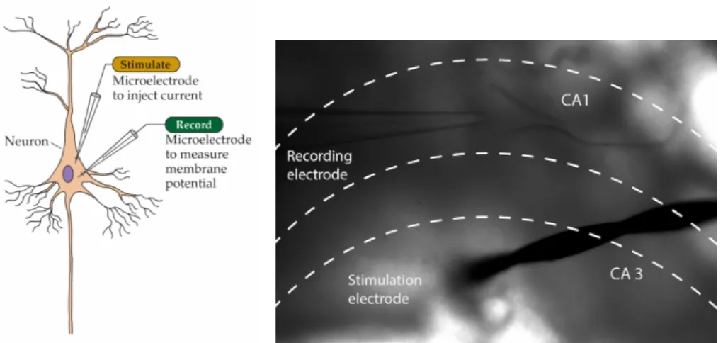
Two common approaches for measuring electrical signals of nerve cells are intracellular (Figure 1.7a) and extracellular recordings (Figure 1.7b). In extracellular electrophysiological measurement, an electrode is placed at the proximity of a cell for detecting its activities and in intracellular recording, the electrode is implanted in the cell [3]. Extracellular recording moni-tors the extracellular electric field, local field potential (LFP) with submillisecond temporal resolution and it can be used as a facet of the neuronal communication. A major benefit of this method is it well known biophysics of its measurements. Extracellular field results from the superposition of overall contributions of any excitable membrane such as dendrite, soma, axon etc., transmembrane currents and electrical signals. Therefore, any transmembrane cur-rent results in intracellular and extracellular voltage deflection. The waveform characteristics of LFP is proportional to the contribution of sources and and depend on the brain tissue’s properties [5].
1.2.5 Rebalancing mechanism of ionic concentration
The movement of ions and organic molecules (osmolytes) across cell membranes results in imbalances; in other words, a change in osmotic pressure. By use of channels and transporters, osmolytes, and as a result water, move to rebalance the initial concentrations (Figure 1.8). The water flux to rebalance the cell, results in cell swelling or shrinkage and is referred to as the mechanism of cell volume regulation [7, 8].
1.2. Generation of electrical signals in nerve cells
(a) Single neuron’s internal record-ing and stimulation. Adapted from [3].
(b) Recording of LFP from mouse’s hippocampus.
Figure 1.7 – Recording of single cell’s activity and local field potential.
Figure 1.8 – Based on the osmotic pressure’s level, water can diffuse though the cellular wall (lipid bilayer) or via the acquaporin channels, channels for cellular water exchange. In addition, it can be diffused against its gradient by cotransporters, such as glutamate using the driving force of Na+in order to move the water and the neurotransmitters against their gradient. Adapted from [7].
1.2.6 Visual cortex neurons and primary visual system’s function
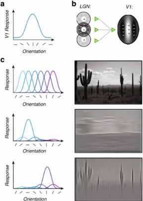
In the primary visual cortex, the majority of neurons are sensitive to the orientation of a visual stimulus [9]. Approximately every sensory neuron in this area is tuned selectively to the ensemble of visual inputs, whether it would be a simple image, such as oriented lines like in Figure 1.9 or a sophisticated visual scene. In primary visual cortex, neurons are responsive preferentially to edges or to particular orientations [10]. The receptive field (RF) is an area of the visual system influenced by the neuronal discharge. The RF is the main structure for studying the physiology of neurons with visual response, since it transforms the visual image to neuronal activity as an inherent function of space-time domain. The RF is mapped using the powerful technique of white-noise analysis to characterize RF for neurons spatio-temporally. In the visual system, the information is transferred from retina through the lateral neniculate nucleus (LGN) to the visual cortex, in a sequential manner. Figure 1.9b presents one of the main configurations of spiking neurons. The organization of retinal ganglion cells and LGN
neurons is approximately circular. In the center-surrounded configuration the polarities of center part and surrounding part are reversed. In this configuration, the RF center responds to bright stimuli (center ON, positive sign) and the surround responds to dark stimuli (center OFF, negative sign). In simple cells, most of the geniculate input is spatially oriented (Figure 1.9c) and is transferred to the primary visual cortex and the elongated subregions response to bright or dark stimuli [11, 12].
Figure 1.9 – a) An example of a typical model of orientation selectivity tuned to a specific function. In this example neuron has a preference of vertical orientations. The orientation tuning’s bandwidth is in the range of 30–40°. b) Sensory neurons in V1, in all the possible ways of orientation are selective. The combination of their activities gives the ability of analyzing visual scenes. As an example, for the desert scene, channels that are selective to horizontal orientations respond to the clouds. Channels that are selective to vertical orientations respond to to the cacti. The combination of their activity, makes us enable to detect all the elements in the scene. c) A model presenting excitatory convergence of orientation selectivity. In this model, three LGN neurons and their circular RF are illustrated. They lie vertically next to each other. The afferents from LGN cells converge to a V1neuron; this effect shows the
orientation selectivity. In this example, it applies for vertically oriented contours. Adapted from [10].
1.3 Label-free and fluorescent indicator-based optical recording in
neuroscience
Optical recording of neurophysiological activity is done using imaging techniques (a.k.a. functional imaging), mainly using two methods; label-free method, including optical imaging of fast [13] and slow intrinsic signals recorded from changes in the optical properties of
1.3. Label-free and fluorescent indicator-based optical recording in neuroscience
brain tissue [14] and fluorescent imaging of different ions labeled with fluorescent indicator dyes [15].
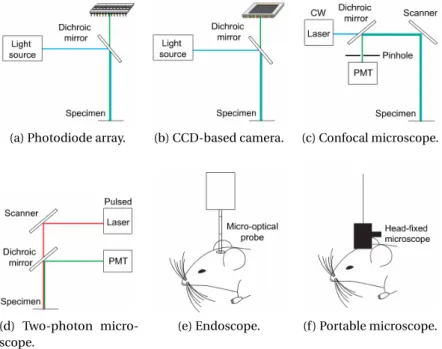
1.3.1 Common imaging devices and light detectors
Figure 1.10 illustrates the major instrumentation types of imaging used in biology. The light sensing device is usually mounted on a microscope in combination with a light source. The type of light source combination depends indeed on the application. The light source is used for the excitation of fluorescent indicators and lightening samples. Two imaging approaches (Figures1.10a and b) involve wide-field microscopy [16, 17], one in combination with multi-pixel photodiode arrays (Figures1.10a) and other in combination with intensified CCD and CMOS cameras (Figure 1.10b) [16]. CCD cameras comprise of densely packed multi-pixel photodiode arrays and in contrast to classical multi-pixel photodiodes, they comprise of a serial signal read-out mechanism. The utilization of photodiode array method is rare, since they provide a relatively low spacial resolution, however they are characterized by a very high speed and dynamic range. On the other hand, modern cameras provide a high spatial and temporal resolution but the serial read-out mechanism limits their temporal resolution relatively and they have a high noise level [16,18]. In order to image the activities of fluorescent indicators deeply in the brain, confocal (Figure 1.10c) and two-photon microscopy (Figure 1.10d) are the most commonly used methods in fixed-position microscopy. There exists specialized tools for the fluorescent imaging of freely moving animals also, such as endoscopic and portable head-mounted microscopic approaches (Figures 1.10e,f ) [16].
(a) Photodiode array. (b) CCD-based camera. (c) Confocal microscope.
(d) Two-photon micro-scope.
(e) Endoscope. (f ) Portable microscope.
1.3.2 Optical and fluorescent indicator technology
One of the most important aims of neuroscience is the understanding of nervous system’s information processing and encoding from cellular to circuit level. The tremendous develop-ment of optical and fluorescent indicators for reporting neuronal functions has enabled this field to monitor activities of ions and ion channels in any region of interest in the brain. The indicators can be divided into two groups, chemical and genetically encoded indicators. The chemical indicator, which is the traditional kind, has been developed initially for in-vitro appli-cation, then its utility was expanded to in-vivo appliappli-cation, giving the possibility of targeting a single cell by injection techniques. Genetically encoded indicators, broadened monitoring functional neuronal activities enormously by providing the possibility of targeting a specific type of cell or ion channel in any region interest in the brain for visualizing activities. These indicators can be grouped based on their target into two sets: optical and fluorescent indica-tors for monitoring ion channel activities such as voltage or Ca2+channels and for visualizing concentration gradients of specific type of ions, such as Ca2+, K+, Na+etc. [15, 16, 19].
1.3.3 Optical imaging of fast intrinsic signals
Hill et al. [20] in the pioneering description of fast intrinsic optical changes indicated that they take place coincidently with neuronal activity. These fast changes occur during the voltage changes (polarization changes) when action potential happens, which can be probably due to the reorientation of the membrane proteins. Light detection in label-free optical imaging is traditionally performed by CCD cameras in combination with a wide-field microscope [21]. This technique lets to image the functional mechanism of optical changes of the brain tissue with a spacial resolution of 50µm. This current technology is still limited for doing more investigation of the optical changes of a single neuron during polarization [22].
1.3.4 Optical imaging of slow intrinsic signals
Slow intrinsic optical changes can be detected more easily using CCD cameras in any region of the brain. These signals arise from cell swelling and the superposition of several sources that contribute in their formation including electrical, majorly action potentials and multiple optical processes [6], such as metabolic activities that cause molecular oxidation, blood volume changes chromophore redox and light scattering etc. [14].
1.3.5 Comparison of label-free optical recording and fluorescent imaging
Fluorescent indicator imaging technique and label-free optical imaging method have their advantages and disadvantages. Their major difference is the time resolution of the signals, which concerns slow intrinsic optical changes and fast signals with submillisecond resolution arsing from fluorescent indicators. In addition, the constraints in the technology for studying fast intrinsic optical changes should be taken intro account. However, each of these signals
1.4. Organic optoelectronics
present different information about various kinds of neuronal and circuit functions; thus, replacing one by another is not the case. In addition, the advantage of optical imaging of the intrinsic optical changes is that in contrast to using dyes, problems such as photo-dynamic and -bleaching damages, as well as pharmacological secondary effects do not exist [22].
1.4 Organic optoelectronics
Organic optoelectronics field has received a tremendous attention for its plethora of appli-cations in organic photovoltaics [23], light-emitting diodes, organic photodetector for imag-ing [24, 25] and biomedical utilizations [26]. This technology notably offers the possibility of low-cost fabrication, modifiability of chemical and physical characteristics through molecular synthesis and design. Also they provide the ease of fabrication, which is mainly due to the pos-sibility of the solution deposition of active materials in the room temperature from very small (µm-feature) to large area flexible substrates [27]. One of the most innovative technologies of organic optoelectronics is sensors based on OPD [28], which has illustrated a high sensitivity. The active layer of such devices (like a typical architecture of organic photovoltaic devices) is composed of an electron donor and an electron acceptor material, where the electron donor is a semiconducting polymer with a low ionization potential (IP). In most cases, the electron acceptor material is a small molecule, such as fullerene derivatives with a high electron affnity (EA), but it can be also another conjugated polymer or a semiconducting metal-oxide, which is referred to hybrid devices [29–31]. Other photovoltaic device technologies use small organic molecule as electron donor material. Kallmann and Pope in their early work, back in 1959, presented an early organic photovoltaic made from anthracene [32]. Today, bulk hetero-junction (BHJ) structures [23, 33, 34] based on small-molecule photovoltaics present a power conversion efficiency (PCE) above 10% in single-junction binary devices (comprising of single donor-acceptor (D-A) materials) [35–37]. These improvements in the device performance is due to the design and synthesis of novel D-A polymers, illustrating optimized energy levels and band-gaps in order to reach high PCE [38–44].
1.4.1 Conjugated polymers
Polymers used in photodetector applications consist of a fully conjugated backbone with single or double bonds that alter [45, 46]. Figure 1.11 shows the conjugated polymers used in this thesis. Single and double bonds’ alterations enable the delocalization of electrons across the polymer’s backbone, due to the overlap ofπ-orbitals. As result, semiconductors consist of a highest occupied molecular orbital (HOMO) and a lowest unoccupied molecular orbital (LUMO). The energy difference between HOMO and LUMO defines the minimum excitation energy of an electron and the semiconductor’s band-gap. In conducting materials, such as metals, there is a small energetic difference between the valance and conduction band. Hence, they do not have band-gap. In insulating materials, the difference in the energy levels is too high. Therefore, the electron excitation form HOMO to LUMO is difficult [47].
Semiconduc-(a) P3HT (b) XPL6 (c)
poly(3,4ethylenedioxythiophene) (PEDOT):poly(styrene sulfonate) (PSS)
Figure 1.11 – Conjugated polymers mentioned in this thesis.
tors, in natural state behave like insulator materials, but doping these materials makes them electrically conductive [48]. Development of polymers for photodetector applications has led to complicated chemical structures (Figure 1.11). Aromatic units is the basis of plenty of conjugated polymers. These units allow for the ease of chemical and physical modifications and other characteristics, such as stability and optoelectronic properties. Aromatic-based polymers possess two types of resonance forms, the aromatic and the quinoid form. The latter describes the polymer structure. For achieving the smallest band-gap, both resonance struc-tures should describe the polymer in an equal manner. In this case, the bond-length difference between single and the double bonds should be small. In order to stabilize the quinoid form, electron donor and acceptor materials should co-polymerize to form the structure [49, 50]. Variations in the polymer’s chemical structure affects several properties [51]. The chemical structure can be divided into two parts, conjugated backbone and the side-chains. These parts can be modified chemically in order to tune the properties. Properties from the point of view of OPD that can be influenced by structural modifications are indicated in below [51]:
• Band-gap and optical absorption. Smaller band-gap gives a higher overlap with the absorption spectra and consequently absorption of more photons. Most of the photons are absorbed in the active layer, which is crucial for the device performance [51]. In conjugated polymers absorption bands are very intense and small [52]. Figure 1.12 illustrates the optical absorption spectra of widely used polymers.
• Energy levels. Beside altering the energy levels in order to define the absorption spectra, these levels should be matched to the energy level of the electron-acceptor material in order to give a high potential difference during charge separation. Energy levels are important for the stability of polymers against photo-oxidation.
P3HT (Figure 1.11a) is a commonly used polymer that is appropriate for the absorption of full spectrum light. XPL6 (Figure 1.11b) is a newly synthesised polymer, which gives a wide bandgap and has a high absorption at blue and green wavelengths, which makes it an
1.4. Organic optoelectronics
Figure 1.12 – Absorption spectra of widely used electron-donor polymers. Adapted from [53].
interesting polymer for detection application in near-UV light spectrum [54]. PEDOT:PSS is highly conducting polymer with a high work-function about 5.2eV that is important for interfacing the active layer and adjacent anode electrode for charge separation.
1.4.2 Fullerene derivatives
Fullerenes are very powerful electron acceptors with excellent electron transport characteris-tics, for this reason they are widely used in OPD technologies. Generally, fullerene derivatives illustrate a limited solubility. For this reason, different functionalized derivatives have been developed [55]. Therefore, this family with different levels of solubility and variety of physical characteristics should be co-polymered with novel low band-gap polymers [56]. PC60B M [55]
and PC70B M [57] are the most frequently utilized fullerene electron-donor materials (Figure
1.13). Other than PCBM, there exists several other fullerene derivatives used in photovoltaic
(a) PC60B M (b) PC70B M
Figure 1.13 – Chemical structure of PC60B M and PC70B M
technology, such as bis-PCBM [58, 59] and I60B A [23]. The chemical structure of PC60B M
and PC70B M are different, due to different amount of carbon atoms comprising the cage.
As Figure 1.14 illustrates, PC70B M has a broader spectrum than PC60B M , for this reason, in
Figure 1.14 – Absorption spectra of PC60B M and PC70B M . Adapted from [56].
1.4.3 Bulk heterojunction
General architecture of OPD device is a multilayer stack (sandwich form) similar to that showed by Tang et al. [60]. This structure (Figure 1.15) consists of a transparent electrode (anode), usually a conducting oxide like indium tin oxide (ITO) [23] or a polymer, such as PEDOT:PSS [34]; D-A light-absorbing layer and a second electrode (cathode). There exists other OPD structures, such as bilayer with the same architecture, but different in the active layer [60]. Figure 1.16a illustrates the energy level diagram of an organic BHJ under illumination. When the device is under illumination, photons are absorbed with an average photon energy, which is larger than the optical band-gap of BHJ (Figure 1.16a step 1). This step is followed by thermalization and the creation of excitons (Figure 1.16a step 2). The interface between D-A materials is responsible for exciton diffusion (Figure 1.16a step 3) and disassociation, which is the formation of electrons and holes. The electrons and holes are transported through D-A layer respectively (Figure 1.16a step 4) and are collected at the electrodes, thereby contributing to the generation of electrical current in the external circuit [52]. Organic semiconductors possess large extiction coefficient, which leads to harvesting light at relatively thin layers with a thickness range of 80–200 nm [52,54]. The organic layer is sandwiched between two electrodes with different work functions. This leads to the formation of a built-in potential and an electric field, which aides the transport of charges [61]. Therefore, after the illumination an interplay of drift and diffusion govern the electron and hole currents in the OPD device [62].
Two important challenges in OPD devices are, exciton dissociation and charge collection at electrode.
• Exciton dissociation. Excitons should be dissociated and diffused in D-A layer rapidly before that they decay to the ground state [63] (charge recombination). Hence, the D-A layer’s thickness should be comparable to the exciton diffusion length [52]. Indeed, the efficiency of the device depends on transportation of holes in the donor component and and electrons in acceptor component of the phase-separated network. Furthermore,
1.4. Organic optoelectronics
Figure 1.15 – General structure of organic photodetector. Adapted from [46].
control of the film’s morphology [64–68] is crucial for the efficient extraction of excitons [52].
• Charge collection. The physics of the interface between D-A layer and the electrodes is complex and much remains to understand. The deposition of the active layer on electrode results in a charge-density redistribution at the interface and geometry modi-fications, which affects the alignment of electronic levels versus electrode’s Fermi level at the organic layer’s frontier (1.16b). Although these interfaces are not very well under-stood yet, but it has been shown that surface modification of electrode by depositing self-assembled monolayers [69] and the application of a monolayer of the polymer polyethylenimine ethoxylated (PEIE) [70] are different ways to enhance the interface of the electrical contact. A monolayer PEIE has shown the modification of the interface of electrode and D-A layer by arranging the charge distribution at the electrode surface [71], leading to the optimization of charge collection [70]. Furthermore, Kieler et al. have presented that the application of PEIE results in the decrease of dark current, hence leading to the increase of OPD device’s detectivity [72].
(a) Bulk heterojunction energy level diagram. (b) Cross-sectional OPD geometry.
1.4.4 Organic photodetector’s electrical characteristics
In dark, the OPD functions as a standard diode, which can be approximated by an equivalent circuit (Figure 1.17a). The equivalent circuit is composed of [52, 73]:
I. A diode characterized with ideality factor n and reverse saturation current density J0in
dark at reverse bias (studied using semi-logarithmic scale of current-voltage (I-V) curve as shown in Figure 1.17b), according to Shockley’s p-n junction theory [74].
II. A photocurrent upon illumination, current source Jph.
III. A series resistance, RS, which should be minimized. This parameter is considered as the
contact resistance between the D-A layer and the electrodes. The buffer layers can help to minimize RSby matching the work functions at their interface.
IV. A shunt resistance, RP, which should be maximized. This parameter is influenced by
leakage paths in the BHJ structure. This involves structural defects, like pin-holes or impurities in the film that lead to charge recombination.
The latter is explained the following mathematical model [73], which describes the I-V be-haviour of OPD: J = J0 · expne(V − JRS) nkBT − 1 o¸ +V − JRS RP − Jph (1.1) where, e the elementary charge, kB is Boltzmann’s contant and T is temperature [74]. In
equa-tion 1.1 [73], the first expression indicates the recombinaequa-tion current, the second expression explains the shunt current and the third one, the photocurrent. From the semi-logarithmic scale curve (Figure 1.17b), the dark current can be extracted, which is measured by apply-ing negative bias (reverse) in dark conditions. Generally, the dark current in OPD devices is intrinsically low, since their conductivity is low, which makes them to reduce the noise dramatically [75]. This parameter should be reduced to increase the sensitivity of the device for detection (detectivity) and to minimize its power consumption. It has been reported that possessing a large offset between the D-A layer’s HOMO level the electrode’s Fermi level is a key parameter in order to minimize the hole injection, leading to decrease the dark current [53]. In the state-of-the-art, 5.5eV is one of the deepest offsets that has been reported [76]. From the linear scale of I-V curve (Figure 1.17c), under illumination, three important parameters can be extracted for device performance evaluation:
I. Short circuit current JSC. Achieved photocurrent at zero volt.
II. Open circuit voltage VOC. Achieved voltage at zero volt. This parameters depends on
the energy difference between the HOMO of donor and LUMO of acceptor, as parameter ∆ shows in Figure 1.16a.
1.4. Organic optoelectronics
III. Fill factor F F . Maximum value of this parameter is a function of VOC and JSCand the
diode’s ideality factor (Figure 1.17c) [52].
(a) Equivalant circuit for modelling organic photodetector.
(b) Semi-logarithmic plot of the same elec-trical characteristics, in forward and reverse bias.
(c) Schematic of IV curves in the dark and un-der illumination.
Figure 1.17 – Electrical characteristics of organic photodetector. Adapted from [52].
1.4.5 Stability and life-time of organic photodetectors
One of the critical challenges that limits the application of OPD, especially in open air is the stability of these devices in presence of degrading elements, such as oxygen, humidity and light. Taking into account the tremendous growth of this field, more stable devices are highly demanding. One challenge in organic semiconductor-based devices is how to unify efficiency, stability and process for the same material [77]. Chemical degradation of OPDs can be mainly considered for the role of oxygen, water and the reaction between the D-A layer with electrode materials. The electron-donor materials used in this thesis are less susceptible to chemical degradation, since probably they do not possess many sensitive oxygen acceptor groups [54, 77]. On the other hand, fullerenes are known for their high degradation potential,
since they have a very high electron affinity [77]. Furthermore, it has been stated that the presence of impurities and moisture within the polymer increase the ionic conduction in the structure and results in corrosion acceleration. Here we divide some of the most important chemical degradation factors (Figure 1.18) into two groups:
Related to the environment:
• Oxygen and water diffusion. Oxygen and water are known to diffuse into the OPD and react with the active materials. Encapsulation impedes this procedure, but current encapsulation materials do not remove this process. There exist different sources of diffusion, such as through the outer electrode via microscope pinholes, release and diffusion of the oxygen from the oxidized sublayers into the active material. Therefore, it is important to remove the microscopic pinholes [77].
• Photo-oxidation. It has been explored that illumination accelerate the oxidation of the organic material’s sublayer. Although several investigations has been carried out to understand the chemical degradation by photoaxidation, however its nature is fairly understood [77].
Related to the device structure:
• Metal electrode. Low work-function electrode tends to react with the oxygen, hence it leads to formation of an aluminium-oxide thin layer, with insulation properties. This thin layer tends to react with the fullerene molecules, hence it decreases the charge transport at the interface of D-A layer and the electrode. This leads to decrease in the device performance. In addition, during the metal evaporation, hot particles can penetrate within the polymer and oxidize it. This results in the reduction of the efficiency of charge transport within the D-A layer and also oxidation of the active material [77]. • ITO electrode. It has been observed that indium diffuses though the device structure
and ends up at the cathode electrode’s (aluminum (Al)) surface. The nature of this phe-nomenon is poorly understood, however it has been stated this is due to the interaction between the PEDOT:PSS layer and ITO. When the water is uptaken from this polymer, it becomes acidic. On the other hand, ITO is sensitive to acidic compounds, which etch it. Therefore, the etching process leads to the release of ITO molecules through the device structure [77].
• PEDOT:PSS interlayer. This layer is used as a hole transporter interfacing between the ITO electrode and the D-A layer. The PEDOT:PSS contains water and after being spin-coated on the electrode, the film is annealed to remove water. However, this polymer is hygroscopic and takes up water from the atmosphere. This leads to fast degradation of the device, by rapid oxidation of the active material and low-work function electrode [77].
1.5. State-of-the-art of optical detection using OPD
Electrical stress is another parameter, which concerns applying of electrical stress in a repeti-tive manner to a device. This leads to inducing traps in the semiconductor, which results in changes in device behaviour [78] and hence its degradation [79]. Currently, one of the most widely-used encapsulation strategies is epoxy, which has been reported to be efficient up to several months [80]. Figure 1.18 illustrates the interaction of degradation parameters within the device structure.
Figure 1.18 – Schematic showing a cross-sectional view of an OPD with possible processes that conspire the degradation of D-A layer. Adapted from [77].
1.5 State-of-the-art of optical detection using OPD
Applications of OPD for optical detection in sensor systems is gaining an increasing attention, especially since the publication of a landmark study by Gong et al. in 2009 [28] that reported an OPD with high sensitivity for detection. Since then, a few reports have focused on the development of OPDs as optical sensors with high sensitivity. Inorganic photodetectors have shown an optical detection capability (detectivity) limited to ∼ 1012 Jones [28] (1 Jones= 1cmH z1/2W ). They have illustrated a relatively a higher dark current density (10−7m A/cm2) than what can be suitable for imaging purposes [24, 81] and a relatively small LDR (lower than ∼ 10−12) at ultra-low light intensities. Non-linearities in dynamic behaviours in response to ultra-low light intensities (pW /cm2-µW /cm2) has also been reported [28, 75]. These devices need a cooling system in order to increasing their dynamic range and to decrease their dark current to gain a higher sensitivity [18, 28]. A high dark current results in limitations in the sensor’s detection ability. Linear dynamic range, which is defined as linear relationship between input and output signal of the device, is important in order to correlate them. These are considered as crucial parameters for the sensitivity/detectivity of any sensor. State-of-the-art of OPDs have presented ultra-low dark current densities (10−15A/cm2), lower than inorganic devices (∼ 1n A/cm2) [24, 82] or have reported relatively high efficiency of more than 60%, which is directly correlated with the responsivity [83–85]. To date, the trade-off
of low dark-current and high device responsivity remains a challenge [72]. One of the most recent reports has tried to address this trade-off by using of PEIE for modifying the interlayer energy level between the D-A layer and electrode. They demonstrate an ultra-low DCD (10−13m A/cm2[72]) and relatively high quantum efficiency. Furthermore, other works have reported DCD quantities between ∼ 10−8[28] to ∼ 10−12m A/cm2[86]. All these quantities have been obtained for devices performing at a high reverse bias range of −2V . Application of reverse bias aims to enhance the device’s charge collection and increasing the sensor’s response time [72, 87]. However, stressing to the device by applying bias leads to increase of the DCD level, changes in the device behaviour and its degradation [78, 79]. Interestingly, it has been shown also that the organic devices present a large linear dynamic range up to ∼ 10−13A/cm2
at ultra-low light intensity of 10−12W /cm2[28, 75]. This quantity of LDR is about 2 orders of magnitude larger than silicon photodetectors [28, 75]. These well-performing parameters have been achieved mainly through chemical modification of D-A layer materials (common approach), changing the device architecture by using a bilayer of active materials [75] and the manipulation of the ohmic contact using PEIE [72].
Another rising effort is to integrate OPDs with very low DCD to integrate in multi-pixel arrays for imaging purposes. Very low DCD is typical for very small active areas (lower than 1mm2) as it has been reported in 2008 [24]. However, for relatively larger areas, obtaining a low dark current becomes challenging. A recent report have illustrated the imaging application of these devices for relatively large areas, ∼ 4mm2, however the reported DCD (10−4m A/cm2
at reverse bias) is relatively high in comparison to other organic counterparts. The state-of-the-art of the biomedical applications of optoelectronic devices will be covered in Chapters 2 and 3. Although a good device performance is desirable in OPD applications, the structural simplicity of OPD should be considered as an important design aspect since it can offer an easy fabrication. This parameter can be achieved by minimizing the number of layers and manufacturing phases, such as annealing-free process or adapting organic active materials to in-air fabrication. To date, Gong and Kieler [28, 72] have reported a well performing minimal device structure, composed of 4 layers electrode/interlayer/BHJ/electrode.
1.6 Aim of the thesis
As indicated in the Abstract, investigation of the OPD performance for optical detection in biomedical applications sets the background of this PhD thesis. This thesis is the first step towards discovering the possibility of utlizing both established active materials and new poly-mers for optical detection in biomedical applications. We aimed to incorporate important parameters of structural simplicity and minimized number of layers for the simplicity of fabrication.
For this goal, in order to evaluate the device performance to measure a broad range of biolog-ical signals, label-free intrinsic optbiolog-ical changes with a wide spectral range and Ca2+signals with a narrow green fluorescent emission profile were assessed.
1.6. Aim of the thesis
low-amplitude optical changes. Established materials, P3HT and PC60B M were chosen for
their low DCD, wide optical absorption and ease of fabrication. Then, the OPD performance was studied by detecting Ca2+signals, which are known for their fast and ultra-low amplitude fluorescent emission. For this aim, a new polymer XPL6 was blended with PC70B M . The
resulting active layer gave a very high absorption spectra, fitting to the emission spectrum of Ca2+signals. The OPD based on this active layer showed to have an ultra-low DCD with a very high detectivity. In addition to the simplicity of the OPD structure, the processing of this active material is enhanced too since it is annealing-free.
Furthermore, the application of OPD devices as a simplified model of the retina to emulate orientation selectivity in neuro-inspired electronics was studied.
![Figure 1.1 – The the principal regions of human’s Central Nervous System. Adapted from [3].](https://thumb-eu.123doks.com/thumbv2/123doknet/8253972.277821/17.892.214.727.651.1014/figure-principal-regions-human-s-central-nervous-adapted.webp)


![Figure 1.4 – Generation of electrical signals arising from transmembrane ion fluxes. Adapted from [4].](https://thumb-eu.123doks.com/thumbv2/123doknet/8253972.277821/20.892.301.540.362.670/figure-generation-electrical-signals-arising-transmembrane-fluxes-adapted.webp)
![Figure 1.5 – Action potential. Adapted from [4].](https://thumb-eu.123doks.com/thumbv2/123doknet/8253972.277821/21.892.269.677.691.1048/figure-action-potential-adapted-from.webp)
![Figure 1.6 – Effect of the reduction of Na + concentration on action potential [3].](https://thumb-eu.123doks.com/thumbv2/123doknet/8253972.277821/22.892.137.713.349.448/figure-effect-reduction-na-concentration-action-potential.webp)