Microcrystalline silicon based thin film transistors fabricated on flexible substrate
Texte intégral
Figure
![Figure 1.8: Applications of flexible displays. a) Electronic paper by HP and ASU [15]](https://thumb-eu.123doks.com/thumbv2/123doknet/7998250.268022/21.918.206.727.107.431/figure-applications-flexible-displays-electronic-paper-hp-asu.webp)
![Figure 1.9 Flexible displays in research laboratories: a) OLED using a-Si:H TFTs on metal foil substrate [18], b) OLED using bottom gate OTFTs on plastic substrate [19], c) EPD using](https://thumb-eu.123doks.com/thumbv2/123doknet/7998250.268022/22.918.229.718.128.542/figure-flexible-displays-research-laboratories-substrate-plastic-substrate.webp)
![Figure 1.13: Density of states in microcrystalline silicon and a-Si:H measured by ICTS [83]](https://thumb-eu.123doks.com/thumbv2/123doknet/7998250.268022/39.918.253.656.115.450/figure-density-states-microcrystalline-silicon-si-measured-icts.webp)
![Figure 2.6: Crystalline fraction of microcrystalline silicon as a function of argon ration in the (Ar-H 2 ) mixture [1]](https://thumb-eu.123doks.com/thumbv2/123doknet/7998250.268022/58.918.287.632.189.533/figure-crystalline-fraction-microcrystalline-silicon-function-ration-mixture.webp)
![Figure 1 a): Transfer characteristic of TFTs using silicon oxide as gate insulator [2], b): Transfer characteristic of TFTs using silicon nitride as gate insulator [2]](https://thumb-eu.123doks.com/thumbv2/123doknet/7998250.268022/94.918.135.724.662.928/figure-transfer-characteristic-silicon-insulator-transfer-characteristic-insulator.webp)
Documents relatifs
LAYOUTISTAKING PLAN GRADING PLAN UTIL'LTIgS PLAN PLANTING PLAN PROFILES CONSTRUCTION DETAILS PART If TX)CATIOB/COVI3R SHEET. S LTE PREPARATION/ CONTRACTOR
L’accès à ce site Web et l’utilisation de son contenu sont assujettis aux conditions présentées dans le site LISEZ CES CONDITIONS ATTENTIVEMENT AVANT D’UTILISER CE SITE WEB.
La Suisse ne participe pas seulement à la définition des objectifs pour l’après-2015, mais également au financement des travaux de l’ONU dans les domaines qu’elle juge
Thus, this paper reports a large area, high sensitivity and high spatial resolution strain gauge arrays using directly deposited µc-Si film as piezoresistive material.. Strain
Further, Michel de Certeau (1990), by acknowledging the possibility for the individual not to execute the action as it is expected, is able to focus on the “manières de
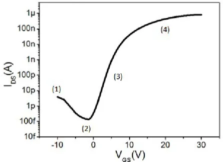
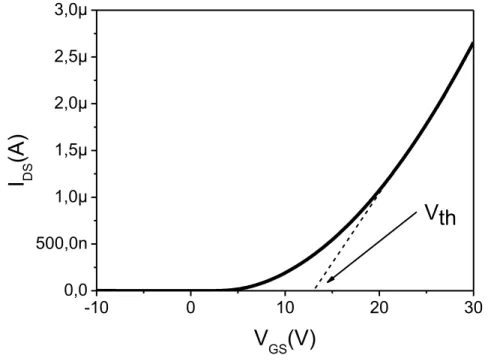
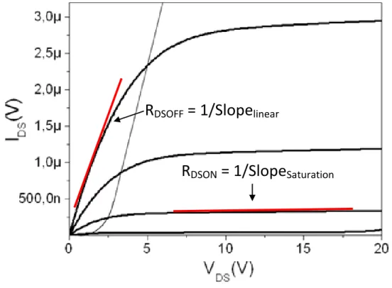
For this reason, we have investigated the properties of TFTs made by a standard a-Si:H top-gate TFT process, but with the a-Si:H layer replaced by microcrystalline ( c-Si:H)
In some cases, this effect is so significant that the hopping barrier seems to vanish and band-like charge transport is then observed (Figure 18). [76, 77] While these
