Multi-MGy Radiation Hard CMOS Image Sensor: Design, Characterization and X/Gamma Rays Total Ionizing Dose Tests
10
0
0
Texte intégral
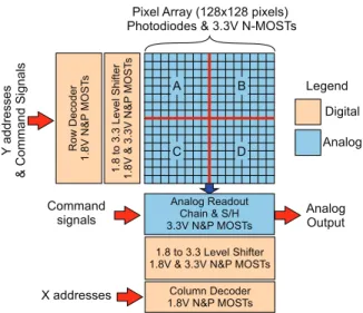
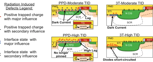
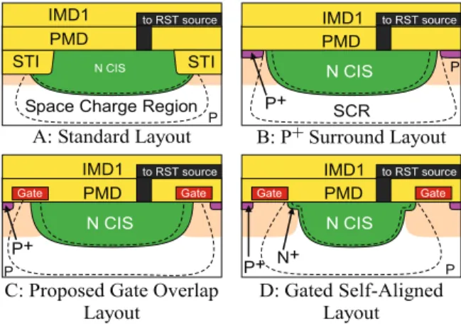
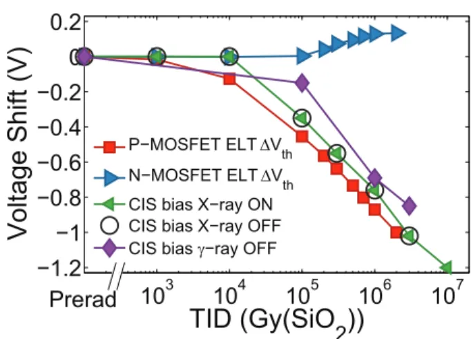
Figure
+5


Documents relatifs