O
pen
A
rchive
T
OULOUSE
A
rchive
O
uverte (
OATAO
)
OATAO is an open access repository that collects the work of Toulouse researchers and
makes it freely available over the web where possible.
This is an author-deposited version published in :
http://oatao.univ-toulouse.fr/
Eprints ID : 11877
To cite this version : Viviès, Noelle and Haussener, Marion and
Welemane, Hélène and Trajin, Baptiste and Vidal, Paul-Etienne
Characterization of an integrated buck converter using infrared
thermography. (2014) In: Quantitative InfraRed Thermography (QIRT)
conference, 7 July 2014 - 11 July 2014 (Bordeaux, France).
Any correspondance concerning this service should be sent to the repository
administrator: [email protected]
Characterization of an integrated buck converter using infrared thermography
by N. Viviès*, M. Haussener*, H. Welemane**, B. Trajin** and P.E. Vidal**
*Univ. Toulouse; INP; ENI de Tarbes, 47 avenue d'Azereix, BP1629, F-65019 Tarbes Cedex, [email protected]
**Univ. Toulouse; INP; ENI de Tarbes, Laboratoire Génie de Production, 47 avenue d'Azereix, BP1629,
F-65019 Tarbes Cedex, [email protected]
Abstract
This study deals with new integrated systems for power electronics applications including wide-gap semiconductors. Integration of Silicon carbide (SiC) components provides for instance new perspectives with higher temperature operating points than conventional Silicon (Si) semiconductors. The present work intends to study an integrated buck converter composed of a Silicon IGBT (Insulated-Gate Bipolar Transistor) and a Silicon carbide diode. By means of infrared thermography, an analysis of the thermal disparities induced within such a hybrid assembly under various electrical loads is proposed, regarding especially the consequences of the electrical power transfer and the spatial distribution of the thermal field.
1. Introduction
The emergence of wide-gap semiconductors allows to design electronic power modules with high compactness and high power density. Indeed, the maturity level of these specific components such as those made of Silicon carbide (SiC) and Gallium nitride (GaN) has strongly increased. Nowadays, they may be used for high integrated industrial applications. In order to optimize integration, higher temperature operating points than for conventional Silicon (Si) semiconductors are considered [1]. Consequently of high temperature, new constrains appear and become critical for power electronics assemblies. Several studies aim at identifying failure modes or critical interfaces [2, 3]. In this field of research, non-destructive characterizations allow to study the mechanisms of degradation without disturbance due to the measurement itself (eg optical microscopy, acoustic microscopy, X-ray, infrared (IR) thermography). Specifically, IR thermography is a convenient and efficient technique for the investigation of systems, even under service conditions. This method has been successfully used for experimental mechanics applications, either for the materials and structures health investigation [4] or the monitoring of dissipative phenomena [5, 6], and seems to be well adapted in the case of electronic power assemblies.
Given the difficulties to obtain full controlled SiC semiconductors at low prices, this technology seems to be intended for high voltage applications. On the contrary, uncontrolled SiC semiconductors are already easily accessible and allow to build efficient and optimized conversion functions [7]. Joint use of a classical controlled Si switch and an uncontrolled SiC switch may induce disparities, including thermal ones, in such hybrid assemblies. In this way, the present work intends to study an integrated buck converter composed of a Silicon IGBT and of a Silicon carbide diode through infrared thermography. In part 2 the electric system and the infrared thermography device are described. A theoretical analysis of Joule losses in the different components of the assembly is then proposed in section 3. These results are compared to experimental measurements and discussed in the final part.
2. System description and experimental device 2.1. Electric system
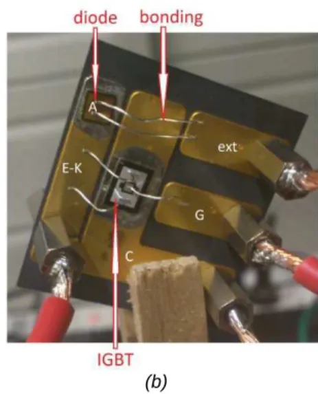
In this study, the power electronic function considered is a buck converter composed of a controlled Si IGBT (1200V – 25A) and of a SiC diode (1200V – 30A). This specific integrated function is completed with an external command circuit and driver for the switchings of the IGBT. The electrical load of the buck converter consists in a resistance of value R=1Ω and an inductance of value L=3mH. On figure 1(a) is depicted the electric operating diagram
and figure 1(b) shows the related power electronic assembly.In this preliminary study, the power electronic assembly is not encapsulated using a dielectric polymer or an external case. Consequently, conduction and dissipations effects
between thermal sources (power electronic chips and wire bondings) and the IR camera are not considered. Power electronic chips are brazed using a Tin-Copper-Silver (Sn-Cu-Ag) alloy on a Silicon nitride Si3N4 substrate covered by Copper power tracks. A thin layer of Gold is added on the Copper tracks as a protection against corrosion.
(a) (b)
Fig. 1. Electric operating diagram (a) and studied assembly (b) 2.1.1. Load current ripple
The switching frequency of the IGBT is set at f =1/T =1kHzso as to get a switching period lower than the time constant of the electrical load τ =L/R=3ms. In addition, it is assumed that the buck converter operates in continuous conduction. In this case, the amplitude of the current ripple in the load during a switching period in steady state operation is approximated by: α Lf RI E Iload = − load ∆ (1)
where E denotes the input voltage and Iload the average load current. The operating point of the load is set constant in this study, by the means of an average current of Iload =8A. The voltage of the power source E is then adapted to the
duty cycle α in order to meet the operating point chosen for the load. The current ripple in the load (1) is expressed according to the duty cycle and average load current:
Lf I Iload =( −α) load
∆ 1 (2)
Given the electrical parameters of the studied system, the maximum value of the ripple current is obtained when the duty cycle tends to 0. In this case, the ripple current is equal to ∆Iload =2.6A. Thus, whatever the operating point considered and therefore the duty ratio controlling the IGBT, the chopper is always operating in continuous conduction.
2.1.2. Root Mean Square (RMS) current
Thermal Joule losses are determined by the value of the RMS current in the load. For a switching period, let us consider the current load iload(t) as the summation of a constant part Iload and an asymmetrical triangular oscillating component with an amplitude of ∆Iload :
[
]
[
]
∈ − ∆ − − ∆ + ∆ + = ∈ ∆ + ∆ − = T T t t T I I I I t i T t t T I I I t i load load load load load load load load load , , ) ( ) ( , , ) ( α α αα α α 1 1 2 0 2 (3)It is shown in that case that RMS value of the current Iload,rms is expressed as follows: 2 2 2 2 2 2 0 2 , ) 1 ( ) ( 1 f L R I I dt t i T I load load T load rms load α − + = =
∫
(4)Thus, the RMS current in the load can be approximated by its average value Iload. The maximum error between the RMS current and the average approximation is then provided by:
Lf R I
errormax= load (1−α) (5)
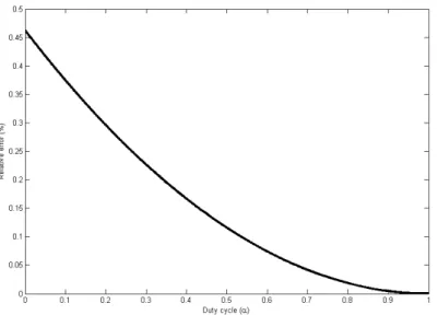
Given the system parameters, the upper bound of the relative error between RMS current and its average approximation theoretically reaches 8.3% when α=0. However, an exact calculation shows that the relative error really obtained does not exceed 0.5% in our case (see figure 2). This study is consistent with the highest oscillations of the load current obtained when the duty cycle tends to 0. So it will be considered in the following that RMS load current is equal to the average load current.
Fig. 2. Relative error on RMS load current
2.2. Infrared thermography
Infrared thermography (IR) is an optical technique for measuring the surface thermal field of a structure. It consists in acquiring the two-dimensional thermal radiation (radiance) emitted by a surface, which depends in particular on the temperature of the material. In addition to its non contact procedure, IR differs from the classical thermography through the range of wavelengths measured.
Obtaining the evolution of the temperature field versus time by a non-intrusive manner as well as the ease of implementation, maneuverability and speed of this technique have led to multiple applications. Compared to conventional techniques, it provides clear advantages in the case of an inaccessible area or a complex environment. This technique is therefore particularly suitable in this case when radiation derives from small parts having a non-zero electric potential and subjected to an electric current flow.
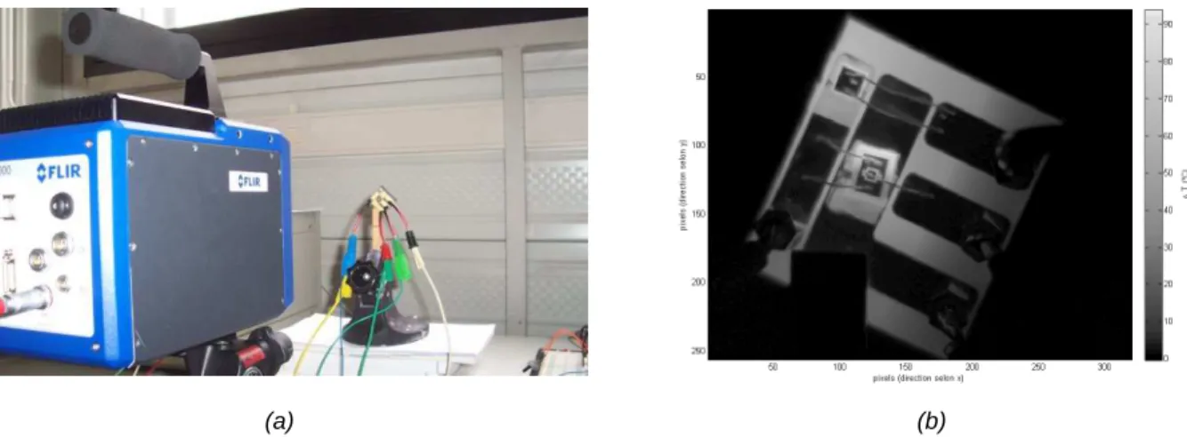
The IR thermography system is composed of a radiation sensor and of a station dedicated to conditioning and formatting the signal, temperature transcription and data recording [8]. The device used here is a FLIR Titanium SC7000 retrofitted camera with InSb sensors, a focal plane of 320×256 pixels and a thermal resolution of 20mK at 30°C. The spectral band corresponds to the interval
[
3.5;5]
±0.25µm (mid infrared), the integration time is set equal to 950µs. For all tests, the acquisition frequency is equal to 10Hz. Camera control and recording are managed by the Altair software, the calibration operation is automatic. In a first approach, the emissivities of the studied components were calibrated using a thermocouple to obtain a surface temperature close to the ambient temperature when the system is in thermal equilibrium without any electrical solicitation. The emissivity of the surface of the IGBT is set to ε=0.75, those of thediode and wire bonding to ε =0.7. The emissivity along wire bonding is assumed constant given the small variations of their surface inclination [9].
Tests were conducted at room temperature and all lights off. To eliminate as much as possible disruptive effects of the environment and highlight thermal changes, a relative analysis on data was performed by subtracting at every step the thermal image of the beginning of the test (∆T =T−T0). Figures 3(a) and 3(b) respectively show the experimental device and a surface relative thermal field on the buck converter.
(a) (b)
Fig. 3. Experimental device (a) and illustration of a surface relative thermal field on the assembly (b)
3. Thermal analysis of the buck converter
3.1. Thermal losses in power electronic components
3.1.1. Conduction losses
As we showed in Section 2, the RMS current in the electrical load is considered equal to its average value
load rms
load I
I , = . Thus, Joule losses by conduction JLcond in semiconductors are obtained from their on-state resistance
on
R and from RMS currents in each switch weighted by the duty cycle:
2 2 1 load diode on diode cond load IGBT on IGBT cond I R JL I R JL ) ( , , , , α α − = = (6) 3.1.2. Switching losses
For the IGBT component, it is necessary to take into account the energy dissipated during blocking Eoff(with slow rate by definition) and switching-on Eon [10]. In a simplified way, it is considered that the current at the switching-on and blocking steps evolves linearly during the switching time (respectively ton and toff times) and that voltage across the IGBT is equal to the input voltage E , it is shown that the dissipated energy during switching can be expressed by
[11]: 2 2 off load off on load on t I E E t I E E = = (7)
In the case of a power diode, switching losses only occur in the blocking step due to reverse-recovery time and associated dissipated energy. However, for SiC diodes, the switching time is very low and the reverse-recovery losses
also decrease [12]. Thus, in this study, the dissipated energy related to the diode switching will only be considered at blocking step (Eoff,diode).
3.1.3. Total losses
Total Joule losses in semiconductors, defined by the sum of conduction and switching losses, are provided in Eq. (8). It is clear that Joule losses in the power components are linear with respect to the duty cycle and therefore with respect to the operating point of the buck converter. It may be noted that, for a given load current and for constant on-state resistances during operation, the losses in the IGBT (respectively in the diode) will increase (respectively decrease) linearly with respect to the duty cycle.
diode off load diode on diode off on load IGBT on IGBT E f I R JL E E f I R JL , , , ) ( ) ( + − = + + = 2 2 1 α α (8)
3.2. Thermal losses in wire bonding
Studies dealing with the robustness of electronic power assemblies often point out that connectivity and especially wire bonding are critical elements for systems reliability [3]. For these connection elements, optimizing their position [13], materials or welding techniques [14] are key factors to improve the performance of an assembly.
In the considered system, power connections are based on pure Aluminium wires of 300µm diameter and an average length of 1.5cm. For the connections between the IGBT emitter and the cathode of the diode and between the anode of the diode and the external connection, two parallel wires are used. Based on the geometric data and Aluminum properties, the wire bonding resistance is evaluated to Rbond =5mΩ. Joule losses in these components can then be expressed by: 2 2 1 2 2 load bond K E load bond ext A I R JL I R JL α α = − = − − ) ( (9)
with JLA−ext (respectively JLE−K) the losses between the anode of the diode and the external connections (resp. between the IGBT emitter and the cathode of the diode). Again, it appears that the Joule losses in the wire bonding are linear with respect to the duty cycle α . Furthermore, since the wire section is constant, it can be assumed that their resistance per unit of length is constant. Thus, in first approximation, the Joule losses per unit of length should also be constant along the wire bonding.
4. Experimental results 4.1. Operating point
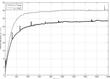
In order to be able to compare the various operating points defined by the duty cycle, the analysis focuses on the thermal steady state of the power electronic components, leading to apply the electrical load on the buck converter for about 30 minutes for each operating point as shown in figure 4 for α =0.5.
As discussed in Section 2, the average load current is kept constant to Iload =8A for all operating points. Furthermore, the variation range of the duty cycle is selected to operate in continuous conduction. Finally, the input voltage is adapted for each duty cycle in order to meet the constraint on the load current. Table 1 summarizes the various operating points selected for this study.
Fig. 4. Thermal variation in semiconductors (duty cycle α=0.5)
Table 1. Input voltage according to the duty cycle Duty cycle α Input voltage E
2 . 0 40V 35 . 0 22.8V 5 . 0 16V 65 . 0 12.3V 8 . 0 10V
4.2. Thermal data processing
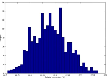
Thermal measurements exhibit an inherent variability related to the camera accuracy and to the thermal ambient noise. Let us consider the relative surface temperature of the diode shown in figure 4. For a thermal steady state, the measured signal consists theoretically in a mean value (useful signal) with added noise. Figure 5 shows the histogram of the relative thermal signal measured. It may be noted that the distribution seems to follow a Normal law with standard deviation σ =0.066, which is consistent with the camera resolution and with experimental conditions.
To improve the accuracy of the thermal measurements, the temperature is averaged over 10 frames at the end of the steady state. This increases the reproducibility of the results by reducing the variance between multiple measurements with the same experimental conditions.
4.3. Thermal behaviour of semiconductors
Figure 6 presents the temperature increase in the steady state at the surfaces of the diode and the IGBT for duty cycles shown in Table 1. These results support the analysis done in Section 3. Maximum temperature variations evolve indeed linearly with respect to α, increasing for the IGBT and decreasing for the diode. Linear interpolation thus
leads to: 4 25 1 9 12 3 31 7 15 . ) ( . . . + − = ∆ + = ∆ α α diode IGBT T T (10)
Fig. 5. Histogram of the relative temperature of the diode in the steady state
Fig. 6. Thermal variations within semiconductors in the steady state according to the duty cycle
Although switching losses depend on the value of the switched voltage, here they can be considered as constant between different operating points. This is due to the low values of input voltages with respect to the ratings of the components in the studied system. Thus, the heating of the IGBT when the duty cycle tends to 0 ( °C
→ =31.3
lim
0
α )
corresponds to the heating induced by the switching losses since no current flows through the IGBT in this case. Similarly, the limit case where the diode is not submitted to any current (equivalently, when the duty cycle approaches 1) provides the thermal behavior related to switching losses within this component, that is °C
→ =25.4
lim
0
α . These results
tend to show that the switching losses in the diode are lower than those in the IGBT. This stands in agreement with the uncontrolled characteristics of the diode switching and also with the technological difference between these two components.
Moreover, it seems that such a difference in the design also leads to distinct overheating observed in the range of operating points. Indeed, it appears in Figure 6 and in the expressions (10) that the absolute value of the increase in the heating rate of the diode is lower than the one of the IGBT. This is explained by the lower on-state resistance of the SiC components [12], which induces a reduction in conduction losses.
In the context of highly integrated power modules, it may thus be preferable to select power components of wide-gap SiC technology in order to limit heat loss and to reduce the volume of the associated cooling systems. Furthermore, infrared thermography provides a relevant tool for identifying the hot spots of the assembly according to the operating point and consequently for designing external heat sinks, regarding both their position and their volume.
4.4. Thermal behaviour of wire bonding
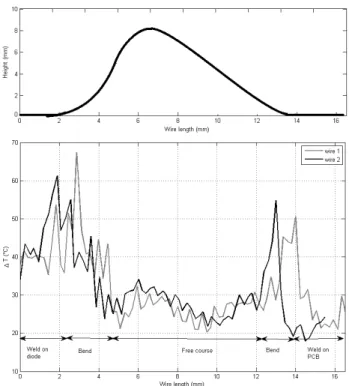
In this study, a special attention was also paid to the wire bonding between the anode of the diode and the external connections. Only the steady state is considered in order to separate two thermal effects: those due to the current flow within the wires, and those associated to the heating of the diode and with the thermal conductivity of the wires. It is assumed that the thermal steady-state is reached in the wires faster than in electronic power components. For a duty cycle α=0.5 , the temperature rise at the diode surface is equal to 7.5°C. Figure 7 shows the geometric profile and the surface thermal field of the considered wires. It is noted that the thermal elevation of the wires is higher than the diode ones, which cannot therefore be regarded at this time as a heat source for the wires. The heating of the wire bonding can then mainly be attributed to the electric current flow.
Fig. 7. Geometric profile and the surface relative thermal field of wire bonding between the anode of the diode and the external connections
Furthermore, the spatial distribution of the thermal field clearly shows heterogeneities along the wire length. Especially, the increase in the temperature is much higher at the diode welding point and at large curvatures of the wire. On the contrary, dissipation by convection is maximum and thermal impact is lower when the wires are far from the substrate and when their curvature is smaller. Thermography allows to show that the wire bonding design exclusively based on Joule losses (9) is not sufficient since nonlinear localized phenomena occur at interfaces. More generally, it should be emphasized that this type of study is of crucial interest for the optimization of these systems as these high thermal heterogeneities can also lead to the damage of the wires and of the conduction paths in case of insufficient cooling.
5. Conclusion
This work has demonstrated the interest of a hybrid assembly between a Si controlled component and SiC un-controlled component within a buck converter. Infrared thermography has been used to characterize the surface temperature
distribution of the assembly, both under active electrical constraints and without contact. The use of a SiC diode leads to a decrease in the overall Joule losses of the assembly, allowing a clear benefit in the design of the heat dissipation elements. Furthermore, thermal analysis allowed to assess the contribution to the dissipated energy during switching and conduction phases within each component. Regarding wire bonding, the proposed method clearly shows hot spots at their edges that should be taken into account for the design of both wires and systems of heat dissipation and cooling. Further works will deal with accurate electrical measurements in order to characterize the dissipated energy during switching of the IGBT and diode but also to specify more precisely the on-state resistance of the components. From the knowledge of the heat loss within the assembly, an equivalent electrical thermal model can be developed to identify and represent the thermal response of the assembly with electric current flow. Furthermore, the thermal distribution along wire bonding will be studied to derive design criteria. A generic model of loss in the power assembly may then be proposed and implemented to correlate the overall performance of the static conversion structure. These thermal studies will finally allow to examine the dissipation and cooling systems and to optimize power structures and their ageing under electro-thermal stresses.
6. Acknowledgements
Authors wish to thank Philippe Lasserre, head of operations for the PRIMES platform of Tarbes [15], which enabled the realization of integrated buck converter. In addition, this study was conducted with the support of a student project within the National Engineering School of Tarbes.
REFERENCES
[1] Funaki T., Balda J-C., Junghans J., Kashyap A-S., Mantooth H-A., Barlow F., Kimoto T., Hikihara T., "Power Conversion With SiC Devices at Extremely High Ambient Temperatures". IEEE Transactions on Power Electronics, vol. 22, n. 4, pp. 1321-1329, 2007.
[2] Ye H., Lin C., Basaran C., “Failure modes and FEM analysis of power electronic packaging“. Finite Elements in Analysis and Design, vol. 38, pp. 601-612, 2002.
[3] Smet V., Forest F., Huselstein J-J., Richardeau F., Khatir Z., Lefebvre S., Berkani M., "Ageing and Failure Modes of IGBT Modules in High-Temperature Power Cycling", IEEE Transactions on Industrial Electronics, vol. 58, n. 10, pp. 4931-4941, 2011.
[4] Maldague X., “Theory and practice of infrared technology for non-destructive testing“, Wiley-Interscience, New-York, 2001.
[5] Chrysochoos A., “Infrared thermography, a potential tool for analysing the material behaviour“. Mécanique et Industries, vol. 3, n°1, pp. 3-14, 2002.
[6] Goidescu C., Welemane H., Garnier C., Fazzini M., Brault R., Péronnet E., Mistou S., "Damage investigation in CFRP composites using full-field measurement techniques: combination of digital image stereo-correlation, infrared thermography and X-ray tomography", Composites Part B : Engineering, vol. 48, pp. 95-105, 2013. [7] Ouwerkerk D., Han T., Preston J., “Efficiency improvement using a hybrid power module in 6.6 kW non-isolated
on-vehicule charger“, 2012 IEEE Vehicule Power and Propulsion Conference, Seoul (Korea), 2012. [8] Pajani D., “Thermographie. Principes et mesures“. Techniques de l’Ingénieur, R 2740, 2001.
[9] Gaussorgues G., “La thermographie infrarouge. Principes, technologie, applications“. Tec & Doc, Paris, 1999. [10] Fock Sui Too J-L., “Caractérisation et modélisation de composants IGBT et diode PiN dans leur environnement
thermique sévère lié aux applications aéronautiques“. Thèse de doctorat, Université de Toulouse, 2010. [11] Dalmasso J-L., “Electronique de puissance : commutation“, DIA Technique Supérieur, Belin, 1986.
[12] Risaletto D., “Caractérisation électrique en commutation de diodes haute tension en carbure de silicium“. Thèse de doctorat, INSA de Lyon, 2007.
[13] Ishiko M., Usui M., Ohuchi T., Shirai M., “Design concept for wire-bonding reliability improvement by optimizing position in power devices“. Microelectronics Journal, vol. 37, pp. 262-268, 2006.
[14] Hamidi A., Beck N., Thomas K., Herr E., “Reliability and lifetime evaluation of different wire bonding technologies for high power IGBT modules“. Microelectronics Reliability, vol. 39, pp. 1153-1158, 1999. [15] http://www.primes-innovation.com