En vue de l'obtention du
DOCTORAT DE L'UNIVERSITÉ DE TOULOUSE
Délivré par :
Institut National Polytechnique de Toulouse (INP Toulouse)
Discipline ou spécialité :
Science et Génie des Matériaux
Présentée et soutenue par :
M. VENKAT SUNIL KUMAR CHANNAM
le jeudi 14 septembre 2017
Titre :
Unité de recherche :
Ecole doctorale :
Synthesis of strongly correlated oxides and investigation of their electrical
and optical properties
Sciences de la Matière (SDM)
Centre Interuniversitaire de Recherche et d'Ingénierie des Matériaux (C.I.R.I.M.A.T.)
Directeur(s) de Thèse :
M. FRANCIS MAURY M. NAOUFAL BAHLAWANE
Rapporteurs :
Mme AUSRINE BARTASYTE, UNIVERSITE DE FRANCHE COMTE Mme ELISABETH BLANQUET, INP DE GRENOBLE
Membre(s) du jury :
M. CHRISTOPHE DETAVERNIER, GHENT UNIVERSITY, Président M. FRANCIS MAURY, INP TOULOUSE, Membre
Mme BRIGITTE CAUSSAT, INP TOULOUSE, Membre
Page
1
Preface
This PhD thesis is dedicated to the physical chemistry of VO2 and V2O5 thin films
and their synthesis through chemical vapour deposition. The research effort shed light at the aspects of VO2 as a metamaterial and study the interplay of electric
and optical properties occurring in this metamaterial region and proposing several innovative applications and proof of concepts. In addition, we report for the first time ever, the nature of thermochromic phenomenon occurring in V2O5,
its mechanism and the cause of this behaviour. The work described in this thesis has been carried out at the materials research department in Luxembourg institute of Technology (LIST) with academic support from CIRIMAT lab at INP-Toulouse.
This thesis is a cumulative article based; the results and discussion are presented as articles that have been published in international peer-reviewed journals. Detailed introduction, literature review and a summary of the experimental work for both VO2 and V2O5 are presented. An extended abstract is
provided in French as an annexe. With this work, I hope to highlight these amazingly responsive systems in a new and unconventional way, and that the outcomes of this research will be useful for future investigation.
C V Sunil Kumar
Page
2
Acknowledgement
Firstly, I would like to sincerely thank my PhD supervisor Dr. Naoufal Bahlawane. I consider myself to be very fortunate to have worked under his excellent guidance. This thesis could have not materialised without his support and encouragement. He has been an impeccable teacher, a wise mentor and above all a great source of knowledge and inspiration. He has taught me to be scientifically curious and methodical in working. Above all he has inspired me each day with his own example of kindness and extraordinary hard work.
I am also very grateful to Prof. Francis Maury, my scientific advisor from INP-Toulouse, for his ever-encouraging comments and scientific discussions. He has been the guiding hand and the father figure to me in all aspects concerning my PhD. His kindness and great belief in me was very humbling and motivated me to approach my research topics with much enthusiasm.
I also thank the Director of the materials research department at LIST Prof. Jens Krisel and the deputy director of the materials group Dr. Damien Lenoble in believing me and for funding my work; without which none of this work produced here would have been possible.
Special thanks to all the amazing co-workers, especially Serena, David, Dheeraj, Alex, Nohora, Vincent, Hameeda and supporting staff that I had the opportunity to work alongside. Life at LIST and Luxembourg in general has been an absolute joy and I got to meet several people and bond many new friendships.
Finally, and most importantly I would like to thank my Science teachers from the school days Dr. Kameswari and Late Sudha Akka as well as my parents back in India to have given me the strength, confidence and instilled in me the scientific vigour, and supported me whole heartedly to follow my dreams.
Page
3
List of publications issued in this work
.
1.
Synthesis of vanadium oxide films with controlled
morphologies: Impact on the metal–insulator transition
behavior.
S Kumar, D Lenoble, F Maury and N Bahlawane. Phys. Status Solidi A,
212: 1582–1587 (2015).
2.
Electrical switching in Semiconductor-Metal
self-assembled VO
2disordered metamaterial coatings.
S Kumar, F Maury and N Bahlawane. Scientific Reports, Article
number: 37699 (2016)
3.
Light modulation in smart Cermet based on phase
change disordered metamaterial.
S Kumar, F Maury and N Bahlawane. (Just submitted) (2017)
4.
An infrared blackboard based on the disordered
metamaterial state of Vanadium oxide.
S Kumar, F Maury and N Bahlawane. (In preparation) (2017)
5.
Visible thermochromism in Vanadium pentaoxide
coatings.
S Kumar, A Qadir, F Maury and N Bahlawane.
ACS Applied Materials
and Interfaces 9 (25), pp 21447–21456 (2017).
6.
Tunable thermochromic properties of V
2O
5coatings.
S Kumar, F Maury and N Bahlawane.
Materials today physics (2) pp
1-5; (2017).
7.
Optical and morphological properties of thermochromic
V
2O
5coatings.
S Kumar, F Maury and N Bahlawane. Data in brief (14), pp 348-353
Page
5
Table of Contents
1. Introduction ... 8
1.2 Vanadium Di Oxide (VO2) ... 9
1.3 SMT in Vanadium Oxides ... 12
1.4 VO2 as a naturally disordered metamaterial ... 17
1.5 Chromic properties of Vanadium Oxides ... 20
2. Synthesis of Vanadium Oxide films ... 25
2.1 Sol-Gel Technique. ... 26
2.2 Sputtering ... 27
2.3 Pulsed Laser Deposition (PLD) ... 28
2.4 Atomic layer Deposition ... 29
2.5 Chemical vapour deposition CVD ... 30
2.5.1 Precursor selection ... 30
2.5.1.1 Inorganic Vanadium Compounds... 30
2.5.1.2 Vanadium Beta-diketonates Compounds ... 31
2.5.1.3 Vanadium Alkoxide Compounds ... 31
3. Experimental ... 33
3.1 Film Deposition techniques ... 33
3.1.1 Chemical Vapour Deposition. (CVD) ... 33
3.1.2 Atomic Layer Deposition (ALD) ... 44
3.1.3 Synthesis of VO2 films ... 45
3.1.4 Synthesis of V2O5 films ... 47
3.1.5 Atomic layer deposition of Al2O3 on V2O5 coatings... 47
3.2 Thin film characterisation techniques ... 48
Page
6
3.2.2 Profilometer. ... 53
3.2.3 X-Ray Diffraction (XRD) ... 55
3.2.4 Electrical resistivity measurements. ... 61
3.2.5 Raman Scattering. ... 63
3.2.6 Optical Spectroscopy... 70
3.2.7 Thermal imaging using a Near Infrared camera. ... 76
References ... 82
4. Results and Discussions ... 96
4.1 Synthesis of Vanadium oxide films with controlled morphologies: Impact on the metal insulator transition behaviour ... 96
4.2 Electrical switching in semiconductor-metal self-assembled vo2 disordered metamaterial coatings. ... 110
4.3 Light Modulation in Smart Cermet Based on Phase Change Disordered Metamaterial. ... 137
4.4 An infrared blackboard based on the disordered metamaterial state of Vanadium oxide. ... 151
4.5 Visible thermochromism in Vanadium pentoxide coatings ... 165
4.6 Tunable thermochromic properties of V2O5 coatings ... 191
4.7 Optical and morphological properties of thermochromic V2O5 coatings ... 208
5. Conclusions and Future Work ... 214
Page
8
1. Introduction
In strongly correlated electron systems, observed electronic and structural behaviours result from the complex interplay between multiple, sometimes competing degrees-of freedom. As a result, these 1,2 materials exhibit a variety of unusual behaviours, such as high-temperature superconductivity, colossal magneto resistance, exotic magnetic, charge and orbital ordering, and insulator-to-metal transitions. 1,2 Oxides of vanadium are typical strongly-correlated materials that have been widely-studied by theoretical and experimental condensed-matter and materials community for more than half a century. Among all the oxides of Vanadium, Vanadium di oxide (VO2) and Vanadium pentoxide
(V2O5) are of particular interest and they enjoy a cult following in the research
community and for good reasons. VO2 and V2O5 have been the materials of
choice to understand fundamental exciting physics and were implemented for the cutting edge industrially relevant applications. 3–9
Chapter 1 of the thesis deals with the basic structures, properties and
background of VO2 and V2O5 followed by a brief review on some novel and
unique functionalities of these materials. The naturally disordered metamaterial nature of VO2 and its impact on the near infrared thermochromic behaviour
combined with the concept of rewritable patterns is introduced. In case of V2O5,
the study is mainly focused on the optical properties and visible thermochromism. The tunability aspect of this property is investigated by different metal ion doping and through selective oxygen deficiency control.
Chapter 2 reviews the synthesis of VO2 and V2O5 by both wet chemical as well
as physical vapour deposition, however special focus is given to the Chemical vapour deposition (CVD) synthesis of vanadium oxide through gas phase evaporation of metal organic precursors.
In depth details about the experimental aspects pertaining to this thesis are provided in chapter 3, whereas results and discussion are detailed
Page
9
The goal of this thesis is to draw the reader’s attention away from the traditional and more often discussed aspects of VO2 and V2O5 and re-introduce these highly
responsive and remarkable materials with a completely new perspective and outlook. The results of this research, many of which believed to be reported for the first time, further strengthen the fact that there is still a lot of untapped potential regarding these two materials.
1.2 Vanadium Di Oxide (VO
2)
VO2 belongs to the class of ― smart material, 10 which generally responds to
external temperature, electric or magnetic fields and/or pressure stimuli. Therefore it has the capabilities of sensing, actuating, and switching, relying on an intrinsic property of the material. These external stimuli bring upon a phase transition in VO2, resulting in large variation of electrical and optical properties.
This phase transition is at the heart of VO2 properties. Thin films and
nanoparticles of VO2 tend to survive the stress generated during repeated cycles
of phase transition better than bulk crystals and are therefore suited for many device applications. 11,12
As far as VO2 is concerned, several crystalline temperature phases have been
reported namely M1, T, M2 and R. The understanding of VO2 and the
metal-insulator transition is even more complicated due to the presence of these additional phases. They appear on application of uniaxial stress or on doping of VO2 with small amounts of Cr, Fe, Al, or Ga of the order of few percent. A
comprehensive phase diagram of Cr doped VO2 is given by Pouget et al. 13–15
According to the authors, Cr-doped VO2 on cooling from a high temperature R
phase, enters the monoclinic M2 phase in a first order metal-insulator transition. On further lowering of the temperature, transition proceeds to a triclinic T phase and finally followed by a first order transition to the monoclinic M1 phase. It is worth noting that the Cr concentration in the films was very low at 0.015%.
Later on, Pouget et al 16 demonstrated that both the M2 and T phases could be likewise stabilized by applying uniaxial stress. It was pointed out that the critical uniaxial stress needed for appearance of the M2 phase is very low, indicating
Page
10
that the difference in free energies of the M1 and M2 phases in pure VO2 are
extremely small. Therefore, M2 and the T phases must be interpreted as alternative phases of pure VO2 whose free energies are only slightly higher than
that of the M1 phase of the pure material. As a consequence, the M2 phase was regarded as a metastable modification of the M1 phase. In contrast, the T phase appears as a transitional state, which displays characteristics of both monoclinic phases.
M1 phase has been the most attractive owing its unique near room temperature insulator-to-metal phase transition and technological applicability. VO2 M1
undergoes a metal-insulator transition to the rutile phase (VO2 R) that occurred at
340 K and ambient pressure. 17 This transition is accompanied by an abrupt change in the resistivity over several orders of magnitude. To better understand this transition, several models have been proposed ranging from Peierls to Mott-Hubbard-type scenarios. All these models point out the role of lattice instabilities, electron-phonon interaction and electron-electron correlations. Yet, all these models are not enough to explain all the phenomena occurring in vanadium dioxide.
The large change in electrical resistivity and transmittance/reflectivity and optical properties during the semiconductor-to-metal (SMT) transition for VO2 occurs
closer to room temperature than any other commonly-known compound and can also be conveniently depressed to about room temperature by doping. 18 The SMT in VO2 has triggered numerous suggestions and their subsequent
realizations for technological applications. These include thermally activated VO2
thin films and nanoparticles for optical switching, 19 resistive switching, 20 thermal relays and energy management for solar cells and glazing 21 ; and sensors and actuators. 22–25 VO2 has also been proposed as the channel layer in
field-effect transistors to produce Mott transistors. 26,27 VO2 thin films also have
potential applications in the millimetre-wave and microwave portions of the electromagnetic spectrum, 28 and have an even greater range of potential applications that are only beginning to be explored. VO2 single-crystalline
Page
11
nanowires with enhanced mechanical strength and stress-resistance. 29 A gas sensor application utilizing the SMT in VO2 has also been realized recently. 30
In a much recent development it was discovered that Metallic VO2 contradicts the
Wiedemann-Franz Law 31 that holds that the ratio of the electronic contribution of the thermal conductivity (κ) to the electrical conductivity (σ) of a metal is proportional to the temperature. The thermal conductivity that could be attributed to electron movement was 10% of the amount predicted by the Wiedemann-Franz Law. The reason for this appears to be the fluidic way that the electrons move through the material, reducing the typical random electron motion. 32
1.3 Vanadium pentaoxide (V
2O
5)
V2O5 is the saturated (highest oxidation state) oxide, and therefore the most
stable one, in the V–O system. It crystallizes with an orthorhombic 33 unit cell structure belonging to the Pmnm space group with lattice parameters a=11.510 Å, b=3.563 Å, and c=4.369 Å. It has a layer-like structure and it is composed of distorted trigonal bipyramidal coordination polyhedra of O ions around V ions. The polyhedra share edges to form (V2O4)n zigzag double chains along the (001)
direction and are cross linked along (100) through shared edges and vertices as shown in figure 1 The distorted polyhedra have a short (1.58 Å) vanadyl bond, [VO]2+, and four O ions located in the basal plane at distances ranging from 1.78
to 2.02 Å. The sixth O ion in the coordination polyhedron lies along the vertical axis opposite to the V–O bond at a distance of 2.79 Å.
Figure 1: Perspective view of two layers of V2O5. V ions are represented as grey balls, O ions as red balls.
Page
12
From a chemical point of view, V2O5 is an excellent catalyst 34 due to its rich and
diverse chemistry that is based on two factors: the variety of vanadium oxidation states, ranging from 2+ to 5+, and the variability of oxygen coordination geometries. It is a brown/yellow solid, although when freshly precipitated from aqueous solution, its colour is deep orange. Due to its high oxidation state, it is both an amphoteric oxide and an oxidizing agent. This structural richness is related to the existence of differently coordinated oxygen ions which provide an important ingredient for controlling physical and chemical surface properties. From the industrial perspective, it is the most important compound of vanadium, being principal precursor to alloys of vanadium and is a widely used industrial catalyst. 35 Another important use of vanadium (V) oxide is in the manufacture of sulphuric acid, an important industrial chemical with an annual worldwide production of 165 million metric tons in 2001, with an approximate value of US $8 billion. Vanadium (V) oxide serves the crucial purpose of catalysing the mildly exothermic oxidation of sulphur dioxide to sulphur trioxide by air in the contact process. 36
Due to its layered structure, V2O5 is a promising material for energy storage
systems and has a high ionic storage capacity. V2O5 has drawn significant
interest in the past decades for its use in several industrially important applications such as electro chromic devices, 37 Gas sensors, 38 and reversible cathode materials for Li+ ion batteries. 39 Due to its high temperature coefficient of
resistance (TCR), vanadium (V) oxide finds use as a detector material in bolometers and micro bolometer arrays for thermal imaging. 40
1.3 SMT in Vanadium Oxides
Many vanadium oxides show SMT/MIT characteristics. These include VO2, V2O3
and most of the magneli phases. 41,42 Figure 2 shows the electrical resistivity versus temperature for several oxides of vanadium, including VO2 and V2O3.
While V2O3 exhibits the highest order of change in resistivity, the low
temperatures at which the SMT takes place make it a non-preferred choice for most of the real world applications. Therefore, VO2 is the most appealing oxide of
Page
13
vanadium that can be exploited in real world conditions, because its SMT occurs closest to room temperature.
Figure 2 : (a) Electrical resistivity across the SMT in various vanadium oxide phases 41 and
(b) Changes in the crystal structure and electronic properties of vanadium dioxide (VO2) occur during its SMT (V blue; O red). Above 67°C (right), large-amplitude, nonlinear lattice vibrations (phonons) lead to a tetragonal crystal structure with mobile electrons (yellow) indicating that the VO2 is a metal. At lower temperatures (left), the electrons are localized in the atomic bonds in the distorted monoclinic crystal structure indicating that the VO2 is an insulator.
In single crystals, the resistivity change reaches a factor of 105 over a
temperature range of 0.1 K 43. Hysteresis associated with this transition is of about 2 K. The conductivity jump and the narrowness of the hysteresis loop are very good indications of how close the stoichiometry is to VO2. Small deviations
destroy the sharpness of the transition and increase the hysteresis width. The crystalline state of the material has an influence too: polycrystalline material will have a broader transition than single crystals. The transition temperature also
Page
14
depends on the crystalline state and oxygen non-stoichiometry. As a rule, the SMT in VO2 is to a certain degree suppressed in thin films as compared to single
crystals.
Despite the many efforts made towards obtaining an understanding of their electronic behaviour, the vanadium oxides still pose many open questions. This fully applies to VO2 as far as the nature of transition is concerned. Some authors
related its phase transition to a Mott-Hubbard scenario, whereas others attributed it to electron-phonon coupling (a Peierls mechanism) on the basis of the crystal symmetry change. There are others who also state that the metal insulator transition in VO2 has a combined nature, having the features of both Mott and
Peierls transitions. The debate seems to be still unresolved.
Peierls transition 44–46 : it is a metal insulator transition occuring by a quasi-one
dimensional metal when it reaches the Peirls temperature Tp. By quasi-one
dimensional one must understand that there is a three dimensional metal where the atoms form chains in one direction that are responsible for the electric conductivity. · Above Tp, the atoms are equally spaced with the lattice constant
“a”. Below Tp, there is a distortion and as a result, the periodicity of the lattice
doubles to 2a because of electron-phonon interactions in the conduction band. This process is called dimerization and happens spontaneously when the metal is cooled down.
In the case of a metal, the bands are only half filled. When the periodicity of the lattice doubles, the brillouin zone boundary also doubles, moving in to the point where the last filled state is . The filled states go to a lower energy and the empty ones to a higher. That process causes a gap in the dispersion relation at the Fermi energy using the perturbation theory. By undergoing that transition, the system gains electronic energy when atoms pair, but it has also a cost of elastic energy to perform the transition. Thus, it only takes place when there is more energy gained that it costs. When we go from rutile to monoclinic we observe a strong splitting of the 2 2band into two narrow sub bands at the lower and
Page
15
dimerization. In addition to that, the V and bands are upshift because of the zigzag-like anti ferroelectric displacement of the vanadium atoms.
So, in the low-temperature M1 structure of VO2 metal-metal dimerization split the
2 2band into bonding and antibonding branches, whereas other states shift
to higher energy due to reduced V-O distances. As a result, insulating state is interpreted as due to a Peierls-like instability of the 2 2 band in an embedding
reservoir of electrons. This Peierls instability allows to explain both the destabilization of the rutile structure in terms of increased metal-metal bonding and the SMT. Even if the strong dimerization, as well as the non-magnetism suggest that VO2 might be a typical case of Peierls insulator, several
experimental works showed that minute amounts of Cr-substitutions, uniaxial stress applied to pure VO2 lead to a new phase M2 in which only half of the
V-atoms dimerize, while the others are contained in chains of equally spaced V-atoms that behave like spin ½ Heisenberg chains. The fact that this phase is also an insulating one suggests that VO2 can be described also as a Mott-Hubbard
insulator.
Figure 3: Peierls transition in a one-dimensional half-filled chain of atoms. Left: Crystal structure and corresponding band structure for temperatures higher than the critical temperature TC. Right: At low temperatures T < TC a periodic lattice distortion doubles the size of the unit cell (Brillouin zone).
Page
16
Mott-Hubbard transition: 47–50
In this theory, the SMT is caused by the strong electron-electron correlation effects. At low temperatures the majority of electrons are localized in the crystal because of the strong electrostatic interaction that prevents them from moving. Electron delocalization is not energetically favoured in Mott insulators compared to a state where electrons are localized in their own atomic states. The competition between the two states determines a critical value above which the crystal is metallic and insulating below. Hubbard introduced a model which gives a meaningful description to the two competing forces presented by Mott. The electron hopping process (which is the kinetic energy term) tends to delocalize the electrons into Bloch states and thus giving a metallic behaviour to the crystal. By contrast, the correlated electron-electron interaction tends to localize the electrons into their own atomic states thus making the crystal an insulator.
A critical question, so far unanswered, is whether the structural and electronic phase transitions in VO2 occur congruently. For non-equilibrium phase
transformations in thin VO2 films, induced by ultra-short laser pulses, it was
reported that the electronic SMT leads the Structural phase transition (SPT), 51 and that the SPT presents a kinetic bottleneck for the transition. It was also observed that for the shortest attainable excitation pulses, a coherent phonon associated with a breathing mode of the VO2 lattice appears simultaneously with
the SMT. 52 Ultrafast electron diffraction measurements on single-crystal VO2
excited by femtosecond near-IR laser pulses demonstrated the existence of transitional structural states with lifetimes up to hundreds of picoseconds. 53 On the other hand, in the case of adiabatic, thermally induced phase transitions, Qazilbash et al. 54 have recently reported an intermediate electronic state characterized by strongly correlated metallic nano puddles with properties distinct from those of the high temperature tetragonal metal. A recent study by Okimura et al 55 of temperature-dependent XRD on thin VO2 films on sapphire (0001)
substrates suggests the possibility that the M2 structure may be an intermediate state during phase transition. Micro-X-ray diffraction studies of epitaxial VO2 on
Page
17
Taken together, these observations indicate the possibility of local energy minima other than the M1 and R phases in the region of strong correlation.
1.4 VO
2as a naturally disordered metamaterial
A metamaterial by definition is a material engineered to have a property that is not found in nature. They are made from assemblies of multiple elements fashioned from composite materials such as metals or plastics. The materials are usually arranged in repeating patterns, at scales that are smaller than the wavelengths of the phenomena they influence. Metamaterials derive their properties not from the properties of the base materials, but from their newly designed structures. Their precise shape, geometry, size, orientation and arrangement gives them their unique properties capable of manipulating electromagnetic waves: by blocking, absorbing, enhancing, or bending waves, to achieve benefits that go beyond what is possible with conventional materials. Appropriately designed metamaterials can affect waves of electromagnetic radiation or sound in a manner not observed in bulk materials. 56 Those that exhibit a negative index of refraction for particular wavelengths have attracted significant research. 57 58 Potential applications of metamaterials are diverse and include optical filters, medical devices, remote aerospace applications, sensor for electromagnetic detection and, smart solar power management. 59,60
The phase changing nature of VO2 has certainly drawn the interest of many
research groups to investigate VO2’s electrical and optical transitions to couple
with existing metamaterial concepts to enhance and tune the exotic properties. However, it was not until recently that VO2 by itself was recognised as a naturally
disordered metamaterial. 61–63
In a narrow range of temperature, between the fully semiconducting and fully metallic phase, there exist third intermediate states of VO2, where both
semiconducting and metallic phases co-exist. This intermediate region was termed as an Inhomogeneous composite medium composed of metallic and insulating domains. Using a “composite medium model” the author 53 described
Page
18
exceeds the transition temperature (Tc) the conducting clusters become larger and form conducting path throughout the film as shown in figure 4.
Figure 4: Schematic diagram of the SMT in VO2 film. The metallic domains start to form nucleation droplets in the film surface sporadically (a), as T approaches TC (b), the domains grow larger and start to form clusters as T increases further. Above TC, the metallic domains form an infinite cluster (c) 64
Later the same region of phase co-existence is also been referred to as monoclinic and correlated metal (MCM) by Kim et al. 65 and strongly co-related metal by M. M. Qazilbash et al. 66 The shaded region in figure 5 represents this state in VO2 over a finite temperature range in the transition region.
Mikhail A. Kats et al. 62 coins the term “naturally disordered metamaterial” and stated thatin this transitional state, the film comprises nanoscale structures of metallic- and insulating VO2, and the resulting effective medium behaves as a
tuneable disordered metamaterial.
Nanoscale inclusions of the metallic phase emerge in the surrounding insulating-phase VO2, which grow and connect in a percolation process, eventually leading
to a fully metallic state at the end of the transition. These metallic inclusions are much smaller than the scale of the wavelength at infrared frequencies (> 800
Page
19
nm), and thus VO2 can be viewed as a natural, reconfigurable, disordered
metamaterial with variable effective optical properties across the phase transition. This metal-dielectric phase co-existence within the phase transition results in widely tuneable optical properties; in fact, the naturally occurring nanoscale structures in the SMT region can be viewed as a reconfigurable disordered metamaterial. The SMT has been utilized for optical switching.
The metamaterial region or the region of phase co-existence opens new opportunities to investigate VO2 in a new perspective. The plethora of interesting
physics that VO2 offers makes it an ideal system for more exotic applications that
have not been fully explored yet. This thesis aims to shed light at the aspects of VO2 as a metamaterial and study the interplay of properties occurring in
this metamaterial region like thermally triggered electrical switching and the
ability to tune the hysteresis amplitude by selective temperature inputs within the hysteric region ultimately leading to control and stabilise the system at highly insulating or conducting phase at the same temperature by employing restrictive temperature modulation.
Figure 5: The phase diagram of VO2 and the resistance-temperature curve showing SMT. The shaded area highlights the region of the phase diagram in which the strongly correlated metal (SCM) 67 or what we refer to as the metamaterial region.
Page
20
1.5 Chromic properties of Vanadium Oxides
Vanadium oxides are popular not just for the host of exciting structural and electrical properties that they offer, but also due to the numerous changes occurring in the optical properties. Interaction of light with vanadium oxides has sparked immense interest in the research community for both VO2 and V2O5.
VO2 is famous for its property of undergoing thermochromic transition to
significantly reflect NIR radiation upon heating beyond its phase transition temperature. In the semiconducting state, it allows transmission of IR radiation and in the metallic state it switches to IR reflective state. This property has sparked a great deal of research in developing VO2 as smart window coatings for
energy efficient buildings and IR reflective devices, thermal cameras, optical modulators etc. All these applications take in to account the phase change occurring from semiconducting to metallic phase.
Probing the physics of this intermediate state is still at an early stage because the material quality of VO2 films has only recently been improved to the point where a
complex region such as the intermediate state of the phase transition can be explored with reproducibility. The SMT in this material has been known for over 50 years; careful thermal profiles and composition control are required to obtain reversible transition properties. Studies on thin film VO2 with reproducible
phase-transition properties can be considered an emerging field, and within that, the intermediate state (i.e., a mixture of metallic and insulating states) is now being recognized as an opportunity, especially given recent interest in metamaterials that often require composite structures comprising domains of sub wavelength dimensions with vastly different optical properties.
Some pioneering work has been done in this regard by M. Kats 68 who demonstrated a perfect absorber at wavelength of 11.6 μm comprising an ultra-thin film of VO2 on a sapphire substrate. The coatings can be tuned into the
perfect absorption state by varying the temperature near the SMT. In this transitional state, the film comprises nanoscale structures of metallic and insulating VO2, and the resulting effective medium behaves as a tunable
Page
21
(figure 6 a). The interaction of light with VO2 and the underlying sapphire
substrate results in essentially complete absorption of the incident light because of critical coupling.
Figure 6: (a) reflectivity spectrum at temperatures from 297K to 360 K. At 343 K, the reflectivity drops to 0.0025 at 11.6 um. (b) The integrated emissivity of the VO2-sapphire sample over the 8 to 14 um wavelength range. 69 The continuous and dotted lines in (b)
represent the heating and cooling stages of the cycle respectively.
Using the same principle of changing the temperature of VO2 in the vicinity of
SMT, it was observed that there exists a certain region where the metallic inclusions form a specific order through which VO2 undergoes perfect thermal
emission and large broadband negative differential thermal emittance. 70 Geometries incorporating VO2 with optical resonances in the infrared is promising
for a wide array of applications calling for tunable infrared emissivity, narrow-band perfect blackbody like emission (figure 6b), negative differential thermal emittance, emissivity hysteresis, or some combination thereof. By controlling the temperature inputs, tunable emissivity coatings can be produced that can change their thermal emissivity to any value between 0 and 1 instantaneously for extended periods, this kind of precise control in emissivity is incredibly useful for solar selectivity and thermal management in space applications.
Page
22
Figure 7: Infrared images from a thermal camera shows reversible patterning on a VO2 surface using a laser to draw (i) lines and (ii) dots. (a) VO2 film is maintained at a steady state temperature of 66.5oC, upon laser irradiation the temperature is instantaneously increased for about 4-5 oC causing localised phase change from a high emissive state to low emissivity state (b)(c). Due to the intrinsic hysteretic behaviour of VO2, the patterns remain without any degradation. Increasing the temperature of the whole film and bringing back to the steady state (d) & (e) erases and resets the VO2 film.
As another example from the work as part of this thesis shown in figure 7, the controllable emittance can be utilized to make a rewritable infrared ‘‘blackboard’’ by keeping the entire sample at the phase-transition temperature and using a cold or hot probe (such as a laser beam or soldering iron) to ‘‘write’’ patterns by thermally induced localized change of emissivity. These persistent patterns could be viewed with a thermal camera but would otherwise be invisible. A digital version of this device can be used as a rewritable infrared identification tag.
Page
23
These patterns or images show in figure 7 “written” on VO2 also act as dynamic
conducting pathways in a highly resistive semiconducting matrix. This opens up a whole new way of utilizing reversible patterning and also in designing variable Meta structures and their investigations for exotic applications that are only limited to one’s imagination.
V2O5 on the other hand also exhibit interesting chromogenic properties like
electrochromism and photochromism. Electrochromism 71,72 is the phenomenon displayed by some materials of reversibly changing colour by using bursts of charge to cause electrochemical redox reactions in electrochromic materials. Due the layered structure, V2O5 easily accommodates guest ions with a consequent
perceptible colour change from Yellow to Blue. This is reversed by applying voltage in the reverse polarity. The process however is not instantaneous.
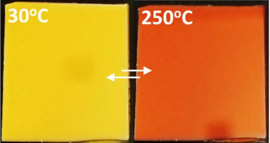
Figure 8: Thermochromic transition of yellow to orange colour in V2O5 coatings 73
Photochromism is a phenomenon of colour change occurring on the surface of the films or material upon exposure of electromagnetic radiation. Shigeru Nishio et al 74 reported the first evidence of reversible visible light photochromism in V2O5. The authors used visible laser light (514.5 nm) to irradiate the oxide, which
turns blue-black upon irradiation due to photo reduction of V5+, and this effect is
confirmed to be irradiation-induced and not heat-induced. However, the irradiation time is around 10 min and to retrieve the initial conditions the oxide must be annealed at 400oC in air.
Page
24
Thermochromism, the property of changing the colour due to the variation in temperature is quite sought after for its various industrially relevant applications. While many metal oxides exhibit thermochromism, the exact mechanism of this reversible transition was not understood completely. V2O5 was also never
mentioned as thermochromic material until now. In this thesis, we report the nature of thermochromic transition occurring in V2O5, its mechanism and
the cause of this behaviour. Therefore, tuning of thermochromic nature was
achieved for V2O5 coatings. Through understanding the fundamentals of
thermochromism in V2O5 we believe, the same can be applied to all
Page
25
2. Synthesis of Vanadium Oxide films
In this section, we concentrate on the different techniques and chemistries used to grow both V2O5 and VO2 films. V2O5 is thermodynamically the most stable
oxide among all other vanadium oxides and is quite straight forward to synthesize. Hence its growth conditions are widely reported and can be generally described as oxidation of VOx films in oxygen atmosphere or ambient air. However, V2O5 films are much sought after for wide variety of application as
previously mentioned. Therefore, much of the research on V2O5 is devoted to
obtaining specific film properties like crystallinity, morphology and microstructure for its intended applications.
Contrary to V2O5, VO2 needs special mentions for being quite challenging to grow
as device grade films or coatings which offers excellent and reliable performance without degrading over time and oxidizing into other oxides or form a mixed oxide phase. The narrow window of thermodynamically favourable conditions that are required for VO2 films imply a strict control over the process conditions.
A brief literature review of the most common fabrication techniques for VOx
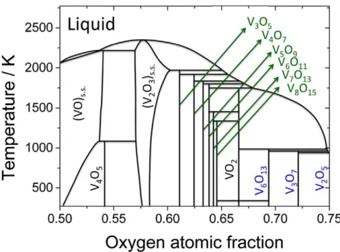
synthesis is provided in this section. Precise control over the purity and the phase of the film is difficult as vanadium oxide forms several stable oxides such as VO, V6O13, V3O5, V4O7 etc. The phase diagram (figure 9) of vanadium oxide system
shows the possible occurrence of nearly twenty stable vanadium oxide phases. The existence of these competing oxide phases offers particular challenge to the growth of both bulk and thin films of VO2. Due to the multi valence state
characteristics of the vanadium ions, oxygen stoichiometry has been also observed to significantly influence phase formation and the properties of the resulting vanadium oxides. With different fabrication conditions, different phases of vanadium oxides including V2O3, [VnO2n-1 (Magneli phase)], VO2, [VnO2n +1
Page
26
Figure 9: Schematic V-O phase diagram showing, Magnéli series, VnO2n+1, highlighted in blue, while the Wadsley series, VnO2n-1, is highlighted in green.
2.1 Sol-Gel Technique.
The sol-gel method has been widely employed for depositing VO2 films because
of its many advantages, such as low cost, large area deposition, and the ease of metal-doping. The sol-gel process is a wet-chemical technique for the fabrication of materials (typically a metal oxide) starting from a chemical solution containing colloidal precursors (sol). Typical precursors are metal alkoxides and metal chlorides, which undergo hydrolysis and polycondensation reactions to form a colloid, a system composed of solid particles (size ranging from 1 nm to 1 μm) immersed in a solvent. 75–77 The sol then evolves towards the formation of an inorganic network containing a liquid phase (gel). Formation of a metal oxide involves connecting the metal centers with oxo (M-O-M) or hydroxo (M-OH-M) bridges, thereby generating metal-oxo or metal-hydroxo polymers in solution, which is then deposited on a substrate or cast in a specific container or used to synthesize powders. The sol-gel approach is an inherently low temperature technique that allows for the fine control on the product‘s chemical composition, as even small quantities of dopants, can be introduced in the sol directly, which
Page
27
gets transferred on the films upon subsequent coating method. 78–82 The precursor sol in case of VO2 is generally deposited on the desired substrate to
form a film (e.g. by dip-coating or spin-coating with a solution of vanadium isopropoxide, VO(OC3H7)3 diluted in an alcohol, (e.g., ethanol or isopropanol),
and then a subsequent annealing process in a reducing atmosphere. A drying process serves to remove the liquid phase from the gel thus forming a porous material, and then a thermal treatment (annealing) may be performed in order to favour further crystallization and densification. The precursor sol in case of VO2 is
generally deposited on the desired substrate to form a film (e.g. by dip-coating or spin-coating). The inorganic sol-gel method using V2O5 as the precursor was
demonstrated by Dachuan et al. 83 According to Livage et al 84 vanadium oxide
gels can be synthesized either via the acidification of aqueous solutions of vanadates, for e.g. NaVO3 or via the hydrolysis of vanadium oxo-alkoxides,
VO(OR)3. Application oriented VO2 films have been made using sol-gel process
by several groups. 85–87 C.B. Greenberg introduced this process for making VO2
as the gelation-hydrolysis method. 88 It has since been found that using the equivalent n-propoxide vanadium compound gives VO2 also, and it is likely that a
wide variety of organometallics and solvents can be used, since the final oxidation state of the vanadium ion depends on the pyrolysis conditions in air rather than the starting material.
2.2 Sputtering
Sputtering, in its many forms, is the most common physical vapor deposition process 89 for growing vanadium dioxide thin films. Vanadium dioxide thin films were first grown by reactive sputtering in 1967 by Fuls, Hensler and Ross of the Bell Telephone Laboratories. 90 They made their films by reactive ion-beam sputtering of a vanadium target in an argon-oxygen atmosphere. Other enhanced sputtering methods used to facilitate the deposition process include RF and DC sputtering and magnetron sputtering. The advantages of sputtering processes are film uniformity, scalability to larger substrate sizes and efficiency of deposition compared to the other methods. The simplest form of sputtering involves a diode sputtering by energetic ions (usually argon ions) from gas-discharge plasma
Page
28
bombarding a target that forms the cathode for the discharge. Target atoms bombard the substrate (the anode), forming a coating. These sources feature a magnetically assisted discharge, in which a permanent magnet defines lines of magnetic flux perpendicular to the applied electric field from the DC or RF source, and is thus parallel to the surface of the target. The magnetic field concentrates and intensifies the plasma, in the space immediately above the target, by trapping of electrons near the target surface. This magnetron effect results in enhanced ion bombardment by the Ar ions, and thus much higher sputtering rates for both DC and RF discharges. After the first experiments in VO2
deposition by reactive sputtering, and further analysis of those samples by Rozgonyi and Hensler, 91 both RF and DC reactive sputtering were studied by Duchene et al. 92 Similar results were obtained in both cases, but since RF sputtering was more suitable for depositing insulating oxides and had the abovementioned advantages over DC sputtering, it became the preferred method for VO2 deposition. To standardize the fabrication of VO2 thin films by sputter
deposition, numerous studies have detailed the influence of sputter deposition parameters, like temperature, oxygen partial pressure, plasma emission ratio of oxygen and vanadium, etc. on the structure, optical and electrical properties of the deposited VO2.
2.3 Pulsed Laser Deposition (PLD)
Pulsed Laser Deposition (PLD), another physical vapor deposition technique, is a comparatively recent inclusion in the world of thin film depositions, and is extensively used in oxide growth. In PLD a high power pulsed laser beam is focused on a target of the desired composition inside a ultra-high vacuum (UHV) chamber. Material vaporized from the target is deposited as a thin film on a substrate, for example Si wafer, facing the target. This process can occur in ultra-high vacuum or in the presence of a background gas, such as oxygen which is commonly used when depositing oxides.
Pulsed laser ablation as a deposition technique was realized in the late 1980s, and it was first used for VO2 deposition by Singh et al in 1993 93. They used a
Page
29
deposition chamber with Ar and O2 (10:1) atmosphere, and a substrate
temperature of about 500oC. The partial oxygen pressure was found to be critical
for the preparation of the pure VO2 phase, for as many as thirteen different
phases ranging from V4O to V2O5 could exist in the system. The as-deposited
samples were annealed for about an hour at the same temperature and pressure to obtain the VO2 that feature sharp SMT. Soon after, Kim and Kwok 94 reported
that they were successful in depositing high quality VO2 films on sapphire by PLD
at high temperature without post-annealing. Maaza et al, 95 was the first to claim room temperature growth of VO2 by PLD, and the as-deposited films showed
rather sharp phase transitions at around 70oC, though it has not yet been
reproduced by any other group. PLD of VO2 thin films has been done on variety
of substrates, including silicon, glass, sapphire, fused silica and quartz. 96 In 2004, Suh et al 51 described the effect of nucleation and growth of VO2
nanoparticles and thin films on the SMT, where the films and nanoparticles were grown by PLD. They showed that the width and shape of the hysteresis is determined by the competing effects of crystallinity and grain size. Recently, in-situ studies of the initial growth phase of vanadium dioxide films using synchrotron-based X-ray diffraction were reported in detail by Pauli et al. 97 They showed that films grown at room temperature are basically amorphous and only crystallize into the VO2 phase upon thermal annealing at 420oC in a background
of O2, with the nano-sized islands sometimes having a preferential orientation
depending on the match with the substrate crystallography. This leads us to the discussion of hetero-epitaxial growth of VO2 on substrates which have good
lattice match with that of VO2 thin films.
2.4 Atomic layer Deposition
Atomic layer deposition involves self-limited surface reactions for the growth of metal oxide by sequentially exposing the surface to metal and oxygen sources one after the other. ALD of vanadium oxides was first studied for catalytic applications and for Li-ion batteries. In these cases, V2O5 was the phase of
interest. 98,99 V2O5 reported starting from vanadyl-tri(isopropoxide) precursor.
Page
30
expected to result in V2O5. In case of VO2 the controlled reduction of the ALD
grown V2O5 yields good quality films but the reduction conditions are often
governed by very narrow operating conditions which makes VO2 synthesis by
ALD difficult. Nevertheless, considerable amount of research has been performed by the group of Detavernier at Ghent university and significant advances were reported 100–103 for the growth of high quality VO2 films by ALD
using relatively new kind of precursors such as tetrakis(ethylmethylamino)
vanadium [TEMAV], tetrakis(dimethylamino)vanadium, [TDMAV], and
tetrakis(diethylamino)-vanadium [TDEAV]. 104,105
2.5 Chemical vapour deposition CVD
Chemical vapor deposition (CVD) is a common industrial process for depositing high quality and high-performance thin films. In a typical CVD process, the wafer (substrate) is exposed to one or more volatile precursors, which react and/or decompose on the surface to produce the desired deposit. Volatile by products are removed by gas flow through the reaction chamber.
2.5.1 Precursor selection
Precursor choice is a main factor in determining the chemistry of the films obtained by CVD and given below are a non-exhaustive list of commonly used precursors and process conditions used by various authors to grow vanadium oxide films.
2.5.1.1 Inorganic Vanadium Compounds
Manning et al. 106 reported the growth of V2O5 at 450–520°C, while VO2 grew
above 500°C. With respect to organometallic vanadium precursors, VCl4 was
found to yield vanadium oxide thin films that showed improved surface smoothness and very acceptable thermochromic properties. Vanadium oxynitrate, VO(NO3)3, was also implemented as a highly volatile single-source
precursor to grow pure V2O5 at 350–500°C. Polycrystalline V2O5 coatings without
preferred orientation were reported at 550–600°C in both cases. Field and Parkin 107 have reported on the CVD of vanadium oxide, under atmospheric
Page
31
pressure, starting from chlorinated vanadium precursors, VOCl3 and VCl4. The
authors noticed that the thermolysis of VOCl3 or VCl4 does not allow the
production of coatings up to 600°C. The reaction of water vapour with VCl4 yields
coatings starting at 450°C, while VOCl3 allows the growth in the entire
investigated temperature range. A focus has been given to the VOCl3/water
system under atmospheric pressure by Manning and Parkin 108. The reaction of water vapor with VOCl3 already occurs at room temperature to yield amorphous
vanadium oxide. The obtained amorphous thin films were converted to crystalline V2O5 upon heating above 240°C. 109 The authors reported the dominant
formation of VO2 above 600°C in the case where the reactive gas contains an
excess of water vapor, while the V2O5 phase prevails in the presence of an
excess of VOCl3 and/or at low deposition temperatures. The deposition of VO2
was also reported starting from the reaction of VOCl3 with water vapor at 650°C.
2.5.1.2 Vanadium Beta-diketonates Compounds
Metalacetylacetonate solutions like V(acac)3 and VO(acac)2, were intensively
investigated for CVD processes under atmospheric and reduced pressures. Vernardou et al. 110 noted the formation of VO2 using VO(acac)2 in methanol at
450°C.The reaction of VO(acac)2 with molecular oxygen under PECVD
conditions has allowed the growth of highly oriented V2O5 thin films at
temperatures as low as 200°C. 111 The use of a vanadyl acetylacetonate precursor, VO(acac)2, with ethanol at growth temperatures from 525 to 530°C
results in VO2. 112,113 The reaction of VO(acac)2 with molecular oxygen at 500°C
114,115 results the formation of crystalline V
2O5.
2.5.1.3 Vanadium Alkoxide Compounds
Vanadium alkoxides 116,117 have been reported as efficient single-source precursors for the synthesis of vanadium oxide films. Mathur et al. 117 have reported on the grown phases starting from the thermal decomposition of vanadium oxo-tri-isopropoxide (VO(OiPr)3) under reduced pressure. The authors
Page
32
reported the formation of a single-phase coating of V2O5 at 500°C. A single
phase of V7O13 was obtained at 600°C, while VO2 was grown at 700°C.
Louloudakis et al. 116 reported atmospheric pressure (AP)CVD using VO(OiPr)3
as a single-source precursor at 300°C. Films obtained were identified as having V2O5 nano-crystals embedded in an amorphous vanadium oxide matrix. Films
grown below 150°C were identified as monoclinic VO2.
Amorphous vanadium oxide, with high performance for lithium batteries, was grown at 105°C using the reaction of VO(OiPr)3 with water vapour. 118 Crociani
et al. 119 have investigated VO(OiPr)3 and reported the possibility of growing
either VO2 or V2O5 at 550°C by adjusting the water and oxygen ratio as the
reactant gas. The CVD of V2O5 was reported starting from VO(OiPr)3, 120 and
Page
33
3. Experimental
The experimental aspects of this research are presented in this section. We discuss the thin film deposition techniques, starting with the basics of chemical vapour deposition and then discuss the Vanadium oxide film synthesis performed on the custom-built reactor nicknamed “sputnik” followed by the industrial scale reactor named MC200 and finally about ALD.
Followed by thin film characterisation techniques used primarily in the analysis of purity, morphology and the SMT behaviour of various vanadium oxide phases obtained. These include X-ray diffraction (XRD), Raman scattering, profilometer, electrical sheet resistance measurements and Scanning electron microscopy (SEM). Followed by the discussion on characterizing the SMT and thermochromic properties of VO2 and V2O5 by optical methods using UV-VIS
spectroscopy and Infrared imaging by thermal camera.
3.1 Film Deposition techniques
3.1.1 Chemical Vapour Deposition. (CVD)
Chemical vapor deposition is a synthesis process in which the chemical constituents react in the vapor phase near or on a heated substrate to form a solid deposit. The number of chemical reactions used in CVD is considerable and
include thermal decomposition (pyrolysis), reduction, hydrolysis,
disproportionation, oxidation, carburization, and nitridation. These reactions can be activated by several methods. The most important are as follows:
Thermal activation: This takes place at high temperatures i.e., 400 -900°C,
although the temperature can also be lowered considerably (300-500oC) if metal
organic precursors are used (MOCVD).
Plasma activation: That typically takes place at much lower temperatures, i.e.,
300–500°C but use plasma to activate the reactant species
Photon activation: Uses shortwave ultraviolet radiation, which can occur by the
Page
34
A CVD reaction is governed by thermodynamics, that is the driving force which indicates the direction the reaction is going to proceed (if at all), and by kinetics, which defines the transport process and determines the rate-control mechanism, in other words, how fast it is going. Chemical thermodynamics is concerned with the interrelation of various forms of energy and the transfer of energy from one chemical system to another in accordance with the first and second laws of thermodynamics. In the case of CVD, this transfer occurs when the gaseous compounds, introduced in the deposition chamber, react to form the solid deposit and by-products gases.
Growth mechanisms
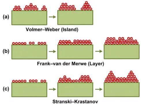
During deposition, adatoms interact with the substrate surface and/or with others adatoms. The strength of interactions defines the growth mechanism of the films, figure 10 shows a schematic of all the models described below.
Volmer-Weber (Island Model)
Three-dimensional growth occurs when adatoms interact preferentially with each other than with the surface. This results in the formation of adatom clusters or islands leading to the growth of rough films over the substrate surface.
Van Der Merwe (Layer by layer model)
Two-dimensional growth occurs when adatoms attach preferentially to the surface sites resulting to the growth of thin-films via layer by layer mechanism (a homogeneous film is formed prior to the growth of any subsequent layer).
Stransky-Krastanov Mechanism (Mixed Model)
A last growth mode involves both Wolmer-Weber and Van der Merwe mechanisms A two-dimensional growth occurs until a critical layer thickness (depending on the surface energy, the lattice parameters of both substrate and film…) is reached. Then, the three-dimensional growth takes place.
Page
35
Figure 10: Different thin film growth mechanisms. (a) island growth model, (b) the layer by layer model, and (C) the mixed growth model. 1
The first step of a theoretical analysis is to ensure that the desired CVD reaction will take place. This will happen if the thermodynamics is favourable, that is if the transfer of energy—the Gibbs free energy change of the reaction (∆Gr) is negative. To calculate ∆Gr, it is necessary to know the thermodynamic properties of each component, specifically their free energies of formation (also known as Gibbs free energy), ∆Gf. The following equation expresses the relationship:
∑ ∑
The free energy of formation is not a fixed value but varies as a function of several parameters which include the type of reactants, the molar ratio of these reactants, the process temperature, and the process pressure. The following equation represents this relationship:
Where ∆Gf is standard free energy of the formation of species, R is the gas
Page
36
As thin films grow, they follow the Gibbs free energy principle. The free energy rule states that the total free energy of a system decreases with increasing size of particles. This leads to the growth pattern described in the figure 11. First, particles nucleate. Next, the individual nuclei grow. As they increase in size, the individual nuclei begin to impinge on each other. The overall system lowers the free energy through coalescence. As growth continues, the remaining area forms channels, leading to a continuous film.
Figure 11 : An overview of the various stages of film growth over the surface in a CVD process.2
A normal CVD process involves complex flow dynamics since gases are flowing into the reactor, reacting, and then by-products are exhausted out of the reactor. The sequence of events during a CVD reaction is are as follows:
Precursor gases input into the chamber by pressurized gas lines.
Mass transport of precursors from the main flow region to the substrate through the boundary layer
Adsorption of precursors on the substrate Chemical reaction on the surface
Atoms diffuse on the surface to growth sites. Desorption of by-products of the reactions
Page
37
During CVD the growth rate of the film is limited by either surface reaction kinetics, mass transport (diffusion) of precursors to the substrate, or the feed rate of the precursors.
Rate-Limiting Steps: CVD growth is controlled by rate limiting steps. The
rate-limiting step is generally determined by either the surface reaction kinetics or by mass transport. A deposition limited by mass transport is controlled by the diffusion of reactants through the boundary layer and diffusion of by-products out of the boundary layer. Mass transport limits reactions when the temperature and pressure are high. These conditions increase the thickness of the boundary layer and make it harder for gases to diffuse through. In addition, decomposition of the reactants is typically quicker since the substrate is at a higher temperature. When mass transport limits the growth, either increasing the gas velocity or rotating the substrate during growth will decrease the boundary layer and increase the growth rate. In the mass transport limited growth regime increases in reactant concentrations will to a point increase the deposition rate. However, at very high reactant concentrations, gas phase nucleation will occur and the growth rate will drop. Slow deposition in a CVD reactor can often be attributed to either gas phase nucleation, precursor depletion due to hot walls, thick boundary layer formation, low temperature, or low precursor vapour pressure.
Precursor flow rate limits the deposition when nearly all the reactant is consumed in the chamber. The flow rate is more important for a hot wall reactor since the heated walls will decompose a large amount of the precursor. Cold wall reactors tend to have higher deposition rates since the reactants are not depleted by the walls.
Page
38
Figure 12: (a) Dependence of CVD deposition rate on temperature and (b) Demonstration of deposition rate on reactant concentration for CVD deposition [3,4]
A plot of growth rate versus temperature, known as an Arrhenius plot, can be used to determine the rate limiting step of a reaction (Figure 12a). Mass transport limits reactions at high temperatures such that growth rate increases with partial pressures of reactants, but is constant with temperature (Figure 12b). Surface reaction kinetics dominates at low temperatures where the growth rate increases with temperature, but is constant with pressures of reactants. Feed rate limited reactions are independent of temperature, since it is the rate of gas delivery that is limiting the reaction. The Arrhenius plot will show where the transition between the mass transport limited and the surface kinetics limited growth occurs in the temperature regime.
In CVD, the reactor configuration also plays a vital role in determining the type of films that one would want to grow. [5] A reactor is a chamber made of a material
that does not react with the chemicals being used. It must also withstand high temperatures. This chamber is composed by reactor walls, liner, a susceptor, gas injection units, and temperature and pressure control units. Usually, the reactor walls are made from stainless steel or quartz. Ceramic or special glasses, such
Page
39
as quartz, are often used as the liner in the reactor chamber between the reactor wall and the susceptor. A substrate sits on a susceptor which is at a controlled temperature.
In a hot-wall CVD, entire chamber is heated as depicted in figure 13 (a). This may be necessary for some gases to be pre-cracked before reaching the wafer surface to enhance their reactivity. Reactors can be constructed either vertically or horizontally and the configuration is decided based on the desired nature of flow. However, reactions usually occur on the walls, and, in most cases, the fraction of the surface area of the reactor covered with deposit can vary and lead to problems when reproducing deposition conditions. In addition, homogeneous gas-phase reactions in the heated gas can occur, which can lead to reduced deposition rates, particle formation and loss of selectivity. For these reasons, hot-wall reactors are used primarily at the laboratory scale to study a given precursor for CVD. They are also used to determine reaction-product distributions because the large heated surface area can consume the precursor completely and provide high yields of the reaction products.
Another type of reactor used to carry out MOCVD is a cold-wall reactor. Where the substrate is supported by a pedestal which acts as a susceptor. The pedestal/susceptor is the primary origin of heat energy in the reaction chamber. Along with the susceptor, the walls of the column are heated to prevent precursor condensation, without impacting the film growth. In contrast the hot wall reactor, the walls of the reaction chamber in a cold-wall reactor are typically made of quartz which is largely transparent to the electromagnetic radiation. The reaction chamber walls in a cold-wall reactor in figure 13 (b), however, may be indirectly heated by heat radiating from the hot pedestal/susceptor, but will remain cooler than the pedestal/susceptor and the substrate the pedestal/susceptor supports.
Page
40
Figure 13: Schematic diagram of (a) hot wall reactor and (b) a cold walled reactor.
The “sputnik” CVD Reactor
For this work, thin films of VO2 and V2O5 were primarily grown using a custom
built MOCVD reactor nicknamed the “Sputnik” with direct liquid injection using a programmable injectors for the precursor delivery. The reactor as shown in figure 14 has four input injectors for precursor delivery. Precise precursor delivery is controlled by setting the injection frequencies and opening times. Rapid vaporisation of the liquid precursor is achieved by maintaining the injectors at 200oC. A vertical heated transport column directs the gas phase reactants
perpendicularly over the silicon substrate with the help of an inert carrier gas like N2 or Ar. The silicon substrate lies on top of the heating plate at elevated
Page
41
essentially call this setup as a warm walled reactor as opposed to a cold or a hot walled reactor.
Figure 14: Computer aided drawing of the CVD reactor labelled with each constituent part.
The quantity of liquid or solution injected/delivered per unit time through the injector is only what is required per unit time for the process and this is adjusted based on the required liquid flow rate. The chemical precursor remains at room temperature as long as it is not required to be vaporized for the process which is advantageous for temperature sensitive precursors. Film deposition can be carried out in a wide range of temperatures ranging from 250 to 600oC at an
operating base pressure of as low as 1.2 mbar.
DLI vaporizers can handle both liquid and solid ALD and CVD precursors. Solid precursors need to be dissolved in organic solvents. The technology is a particularly well suited method for low vapour pressure and poorly thermally stable liquid or solid ALD and CVD precursors.
Advantages of DLI:
Precise measurement and control of the precursor quantity injected in the vaporizer per unit time and by consequence precise control of the vapour flow that is generated