This is an author-deposited version published in:
http://oatao.univ-toulouse.fr/
Eprints ID: 8022
To link to this article: DOI: 10.1109/TNS.2011.2170854
URL: http://dx.doi.org/10.1109/TNS.2011.2170854
To cite this version:
Gaillardin, Marc and Goiffon, Vincent and Girard,
Sylvain and Martinez, Martial and Magnan, Pierre and Paillet, Philippe
Enhanced Radiation-Induced Narrow Channel Effects in Commercial 0.18
μm Bulk Technology. (2011) IEEE Transactions on Nuclear Science, Vol.
58 (p. 6). pp. 2807-2815. ISSN 0018-9499
O
pen
A
rchive
T
oulouse
A
rchive
O
uverte (
OATAO
)
OATAO is an open access repository that collects the work of Toulouse researchers and
makes it freely available over the web where possible.
Any correspondence concerning this service should be sent to the repository
administrator: [email protected]
Enhanced Radiation-Induced Narrow Channel Effects
in Commercial 0.18 m Bulk Technology
Marc Gaillardin, Member, IEEE, Vincent Goiffon, Member, IEEE, Sylvain Girard, Member, IEEE,
Martial Martinez, Pierre Magnan, Member, IEEE, and Philippe Paillet, Senior Member, IEEE
Abstract—Total ionizing dose effects are investigated in
input/output transistors that are fabricated by using a com-mercial 0.18 m bulk process. An enhanced radiation-induced narrow channel effect is demonstrated in N-type metal–oxide semiconductor (NMOS) and P-type metal–oxide semiconductor (PMOS) transistors, leading to a significant threshold voltage shift which may compromise circuit operations. Calculations using a code dedicated to radiation-induced charge trapping in oxides show that the radiation-induced positive charge trapping in trench oxides leads to the modifications of the electrical characteristics experimentally evidenced. Radiation hardening issues are finally discussed as a function of the device geometry and design.
Index Terms—Deep submicron (DSM) bulk technology,
metal–oxide semiconductor (MOS) transistors, radiation-in-duced narrow channel effect (RINCE), total ionizing dose.
I. INTRODUCTION
I
NTEGRATED circuits (ICs) for space, scientific, and medical applications must be tolerant of a wide range of total ionizing dose (TID). During the past five years, most TID effects studies were focused on new technologies, such as fully depleted SOI [1]; FinFETs [2]–[4]; FinFlash memories [5], [6]; or metastable dip random-access memory [7]. On the other hand, TID effects are generally not considered a major issue for design hardening in deep submicron (DSM) complemen-tary metal–oxide semiconductor (CMOS) bulk transistors [8], [9]. However, the continuous shrinking of integrated device dimensions leads to an enhanced susceptibility of transistors due to radiation-induced charge trapping in shallow trench isolation (STI) [10], such as STI sidewall leakage currents and radiation-induced narrow channel effects (RINCE), which was demonstrated for high TID 10 Mrad) [11]. Whereas several studies have been dedicated to STI-induced leakage currents in DSM metal–oxide semiconductor field-effect transistors (MOSFETs) [10], [12], [13], few papers have been published on RINCE and on the behavior of irradiated STIs [14], [15]. Moreover, most of the available results have been achieved on core transistors and only few data are available on I/Otransistors. This is especially true for PMOS transistors, which are commonly assumed as less sensitive to TID. There are two reasons for this as follows.
1) PMOS transistors are not susceptible to sidewall leakage current.
2) The main TID effect on PMOS transistors is thus related to the radiation-induced charge trapping in the gate oxide, which is strongly limited in low-voltage operation DSM transistors due to the continuous thinning down of the gate oxide with the technology integration.
Even so, it was demonstrated that applications for which narrow transistors are needed, such as CMOS image sensors, based on a bulk DSM technology may be sensitive to a much lower TID 100 krad) [16]. Since such transistors are widely used for I/Os or analog applications, studying their TID behav-iors as a function of their geometry and design is thus needed to manage mitigation techniques.
This paper investigates the TID effects in NMOS and PMOS I/O transistors related to the STI. We report NMOS transistor leakage current increase, as usually observed, and unexpected very large RINCE in NMOS and PMOS transistors related to radiation-induced positive charge trapping in STI. The effect of biasing on their degradations is also studied for both MOS transistors types. First, the TID response of the gate oxide is separated to the one of the trench oxide by studying enclosed and open layout transistors, respectively. Then, charge-trapping properties of the STI are analyzed with electrical characteristics measured on field-oxide FETs (FOXFET) along with dedicated self-consistent calculations of charge trapping in the STI on a FOXFET structure. Finally, we discuss the enhanced RINCE sensitivity observed on NMOS and PMOS transistors related to the device geometry and its implications on the radiation hard-ening of modern CMOS ICs.
II. EXPERIMENTALDETAILS A. Test Structures
Elementary transistors were fabricated by using a commercial bulk 0.18 m process optimized for mixed-signal applications and CMOS image sensors. The I/O transistor manufacturing process involves a gate stack made of a 7-nm-thick gate dielectric (processed using a double gate–oxide growth which is named GO2 in the following text), topped by a highly doped polysilicon gate. Adjacent devices are dielectrically isolated by shallow trench isolations (STI) with a thickness of about 400 nm. NMOS and PMOS transistors with various geometries have been achieved: the device widths W vary between 0.24 and 10 m and the gate lengths vary between 0.34 and 10 m.
TABLE I
BIASCONFIGURATIONSDURINGIRRADIATION
All transistors are designed with a standard open layout where the STI circles the entire active silicon area. Additional NMOS transistor designs are also available including one annular en-closed layout transistor (ELT) drawn with the minimum geo-metric rules and one FOXFET. In the FOXFET, a polysilicon gate is deposited directly on the STI which acts as a thick gate dielectric between two Nwell-doped regions making the source and the drain areas of a large transistor. All devices are mounted in standard pin grid-array packages.
B. Experiments
Each transistor was irradiated at room temperature using 10-keV X-rays at a constant dose rate of 100 to reach a maximum total dose of . The total dose was deposited in several irradiation steps which were immedi-ately followed by static electrical measurements performed by using a HP 4145 parametric analyzer. Three different bias con-figurations were applied to the devices during irradiation:ON, OFF AND NON. They are detailed in Table I where bias applied to
source, drain, gate, and Nwell terminals are referenced as , , , and , respectively. The substrate is always grounded during irradiation. The nominal bias voltage for I/O transistors is 3.3 V for the studied technology. The
NON-bias configuration does not correspond to a conventional
circuit case. Above all, it was performed to study the effect of the radiation-induced positive charge-trapping location on the electrical characteristics of MOS transistors. The additional NULL (all terminals grounded) bias configuration during irradiation was also performed on FOXFETs.
III. EXPERIMENTALRESULTS
Since the mechanisms of radiation-induced charge buildup occur in most oxides [17], we thus must consider the TID re-sponse of the gate oxide and of the field oxide of the tested bulk transistors.
A. Contribution of the Gate Oxide to the TID Response of MOS Transistors
Enclosed layout transistors are first characterized under irra-diation to infer the sole TID effect on gate–oxide properties. Modification of the electrical characteristics will be only be at-tributed to the charge buildup in the 7-nm-thick gate oxide. This is justified by the absence of interface between the source-to-drain conduction channel and the trench oxide in the enclosed layout design.
Fig. 1. Drain current versus gate voltage characteristics of an enclosed layout transistor before irradiation (black line) and after (red dashed line).
Fig. 1 exhibits the curves of the NMOS ELT before irradiation (black line) and after a total dose of
(red dashed line). In that case, the device was biased in the
ON-state configuration during irradiation. This type of
config-uration should maximize the positive-charge trapping at the gate–oxide/active silicon interface (only the gate is biased at ; the other terminals are grounded). Fig. 1 shows no suffi-cient radiation-induced change of the electrical characteristics to extract any electrical parameter shift. The radiation-induced charge buildup in the gate oxide can thus be neglected even at a total dose of . No significant discrepancy to this behavior was observed under irradiation for the other tested bias configurations. Results obtained on the ELT highlight the weak influence of charge buildup in the 7-nm-thick gate oxide on the electrical characteristics of the tested bulk transistor.
B. Total Ionizing Dose Effects in NMOS Transistors Designed With an Open Layout
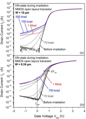
Fig. 2 illustrates a series of subthreshold I-V curves measured on a wide [ 10 m, Fig. 2(a)] and a narrow [ 0.24 m, Fig. 2(b)] open-layout NMOS transistors. These results show that increasing TID leads to the buildup of positive–oxide trapped charges at the Si/STI interfaces. These charges de-crease the threshold voltage of the parasitic lateral transistor. This clearly appears as a shoulder on the I-V curves of both transistors of Fig. 2 at a total dose of about 70 krad . This parasitic lateral transistor induces excessive drain leakage current defined at a gate voltage . Fig. 3 shows the variations versus the total dose for 10 m wide (filled symbols) and 0.24 m narrow (open symbols) transistors irradiated in the three different bias configurations described in Table I. This figure is evidence that theON-state corresponds to
the worst bias configuration during irradiation considering the occurrence of the parasitic sidewall transistor. This parasitic conduction channel increases the leakage current by about three orders of magnitude after 100 krad . On wide transistors [Figs. 2(a) and 3, black squares], the leakage current reaches a maximum at 500 krad before decreasing. This phenomenon may be explained by the following mechanisms: the radiation response of the transistor is first dominated by the radiation-induced positive trapped charge in the STI, causing
Fig. 2. Drain current versus gate voltage characteristics of NMOS open layout transistors at several total dose steps from before irradiation (bold black line) to (red dashed line). curves are presented for wide transistor with 10 m (a) and for a narrow transistor with 0.24 m. (b). Both transistors have a gate length of 0.34 m.
Fig. 3. Leakage current as a function of the total ionizing dose for wide ( 10 m, filled symbols) and narrow ( 0.24 m, open symbols) open layout NMOS transistors. The results are displayed for devices irradiated in theON-state (black squares), theNON-state (red circles), and theOFF-state (blue triangles) bias configurations. All transistors have a gate length 0.34 m.
the occurrence of the parasitic sidewall conduction. For higher TID, this may be counterbalanced by the contribution of the negatively charged interface traps at the silicon/STI interfaces slightly decreasing the leakage current.
Moreover, for a chosen bias configuration, the shapes of the versus TID curves exhibit a TID threshold at which the leakage current increases sharply. This suggests that the trig-gering of the parasitic lateral transistor does not depend on the width of the device but only on the bias configuration used during irradiation. This was previously observed by [11] since
Fig. 4. Negative voltage shift versus total ionizing dose for a narrow 0.24 m) open layout NMOS transistors. The results are displayed for the three bias configurations during irradiation described in Table I. All transistors have a gate length of 0.34 m. Results for wide transistors 10 m are not displayed because the variations are negligible.
the parasitic sidewall transistor should be similar to whatever the width of the transistor is.
The negative voltage shifts extracted by using a constant cur-rent approach (at low ) on narrow NMOS transistors as a function of TID are illustrated in Fig. 4. The results are only presented for narrow transistors 0.24 m since the ones related to the wide transistors 10 m stay within the measurement uncertainties. Here, the response of narrow tran-sistors strongly depends on the bias configuration during irradi-ation as the locirradi-ation of the positive trapped charges is defined by the shape of the electric-field lines in the trench oxide during ir-radiation. So, theNON-state and theON-state appear as the worst
cases from the voltage-shift standpoint. In those cases, most of the positive charges generated during irradiation, which have escaped initial recombination, may be trapped at the STI/ac-tive-silicon boundaries. Positive charges may be trapped in the entire depth of the trench evenly distributed along the source-to-drain conduction channel. This lowers the source-to-body and body-to-drain potential barriers and then the threshold voltage. This phenomenon is known as RINCE [11]. In our case, this RINCE is very intense with a shift reaching about 200 mV at a dose of 100 krad and exceeding 300 mV at larger doses. The gate oxide is not involved in the degradation since wide transistors do not exhibit the RINCE and since no is observed in ELT (Fig. 1).
Each characteristic displayed in Fig. 4 shows two major re-gions. At low dose, below 150 , the negative voltage shift quickly rises, corresponding to an efficient positive charge trapping in the trench oxide which corresponds to the enhanced RINCE. The slopes vary between each bias case during irradi-ation. This may be due to the various locations and densities of the positive trapped charges in the STI which will be further in-vestigated in Section IV using dedicated self-consistent TCAD calculations of charge trapping. This will provide valuable in-sights to explain the behavior of open layout transistors.
At higher total ionizing doses, above 150 krad , each characteristic saturates. This may be due to the buildup of inter-face traps which are negatively charged in NMOS transistors. This competing mechanism is partly screened at low dose but
Fig. 5. Drain current versus gate voltage characteristics of the PMOS open layout transistors at several total dose steps from before irradiation (bold black line) up to (red dashed line). curves are presented for a narrow transistor with biased in theON-state during irradiation. The gate length is 0.34 m.
it may counterbalance the positive charge trapping at high total dose. It may also be due to saturation of the hole traps in this part of the STI. Here again, Section IV, which is dedicated to the radiation-induced charge trapping and interface traps in the trench oxide, will provide additional data to obtain new insights on the charge-trapping properties of the STI.
C. Electrical Performance Degradation of Bulk PMOS Transistors
Most studies on the total dose effects on MOS devices focus on NMOS transistors because they are usually the most sensitive device to ionizing radiation, especially for bulk transistors with a thin gate oxide.
Based on the results presented in the previous part, the pos-itive charge trapping in the trench dielectrics should change the electrostatic potential in the PMOS transistor as well as in the NMOS one. This corresponds to what can be inferred from Fig. 5 where the I-V curves obtained on a narrow 0.24 m) PMOS transistor before irradiation (black line) and after (red dashed line) biased in theONstate are
drawn.
A large threshold voltage shift is observed 440 mV). To our knowledge, such a threshold voltage variation at on a PMOS transistor with a thin gate oxide has never been reported before. In [11], more than 100
were needed to attain such a threshold voltage shift on PMOS transistors designed with a similar geometry , which is limited to 30-40 mV at in [11]).
The threshold voltage shift has been extracted on a narrow PMOS transistor with a gate length 10 m (open sym-bols) and a gate length 0.34 m (filled symbols) as a function of total ionizing dose in Fig. 6. All voltage shift versus TID curves follow a similar trend. It clearly does not depend on the gate length and on the bias configuration during irradiation. With radiation-induced charges being positive as well as the in-terface traps in PMOS transistors, this could explain the overall trend drawn in Fig. 6 in comparison to the behavior observed in Fig. 4.
Fig. 6. Negative threshold voltage shift versus total ionizing dose for narrow 0.24 m) open layout PMOS transistors. Results obtained with two gate lengths are represented: 0.34 m (filled symbols) and 10 m (open symbols). The results are displayed for the three bias configurations during irradiation described in Table I.
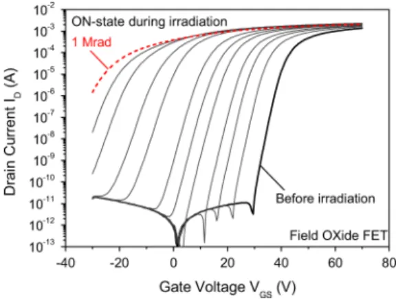
Fig. 7. Drain current versus gate voltage characteristics of a FOXFET at several total dose steps from before irradiation (bold black line) to (red dashed line). The FOXFET was irradiated in theON-state
bias configuration during irradiation ( , other terminals were grounded).
IV. DISCUSSION ON THEIONIZINGRADIATION-INDUCED
EFFECTS INTRENCHOXIDES
A. Insights on the Radiation-Induced Charge Trapping in Trench Oxides: FOXFET Characterization
The FOXFET is a convenient tool to characterize the sole radiation-induced charge trapping and interface traps buildup in the field oxide. As described in Section II-A, the FOXFET is a MOS transistor where the STI acts as a gate oxide in which large radiation-induced positive charge trapping should occur. This leads to a large threshold voltage shift in its I-V characteristics (Fig. 7).
The threshold voltage shift observed in Fig. 7 exceeds 50 V after . In that case, the electric-field lines start from the gate to reach the STI-silicon interface where most of the radiation-induced positive charges are trapped efficiently, modifying the device response. Using other bias configurations during irradiation should modify the radiation-induced charge-trapping location in the STI. This is illustrated in Fig. 8 where negative threshold voltage shifts observed on the FOXFET are
Fig. 8. Negative threshold voltage shift versus total ionizing dose for the FOXFET. Results are displayed for the three bias configurations during irradiation described in Table I: theON-state (black squares), theOFF-state (blue
triangles), and the NON-state (red circles). The additional NULL-state bias configuration (all terminals grounded) performed only on FOXFET is added (green diamonds).
displayed as a function of total ionizing dose and of the bias configuration during irradiation.
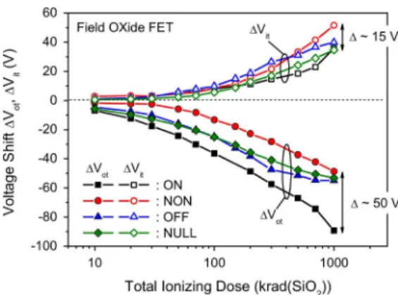
The radiation-induced positive charge-trapping location and density mostly depend on the shape of the electric-field lines in the oxide. The bias configuration during irradiation thus plays a major role in the behavior exhibited in Fig. 8. Results gathered by using theON-state bias configuration do not exhibit a clear
saturation of the radiation-induced voltage shift. By contrast, re-sults obtained using the other bias configurations during irradi-ation all reach a maximum at about 200 . This clas-sical balance effect between trapped-oxide charges and interface traps is maximized in the NON-state (red circles) for which the net influence of each contribution leads to an apparent threshold voltage shift around zero at . This parameter ex-traction may screen a large increase of the subthreshold slope that degrades the I-V characteristics.
Thus, the contributions related to the oxide trapped charge and to the interface traps are now separated [18] in Fig. 9 to weigh up their respective impact on the curves exhib-ited in Fig. 8. The first interesting feature is that the interface traps contribution (in the upper part of Fig. 9) seems less sensitive to the bias state configuration during irradiation than the contribution related to the oxide trapped charge (lower part of Fig. 9). The maximum difference between reaches 15 V at between theON-state (black squares) and
theNON-state (red circles) when this difference between
values exceeds 50 V at . If the large discrepancies measured between would have been expected as a func-tion of the bias configurafunc-tion during irradiafunc-tion, it is not straight-forward concerning those related to . It is especially true for voltage shift observed using theNON-state for which a
nega-tive bias is applied on the gate electrode. In that case, one could expect that no buildup of an interface trap should occur.
The TID effects on MOS structures were widely studied in the literature [19]–[26], including the mechanisms responsible for the generation of interface traps under irradiation [27]–[31]. Even if the details of the interface traps generation still need to be investigated, especially in thick oxides, a consensus was
Fig. 9. Voltage shifts versus total ionizing dose associated with the oxide-trapped charges and to the interface traps for the FOXFET. Results are displayed for several state bias configurations during irradiation: theON-state (black squares), theOFF-state (blue triangles), theNON-state (red circles), and theNULL-state.
reached on the overall physical mechanisms which govern the buildup of interface traps at silicon/oxide interfaces under ir-radiation. First, it is not directly caused by ionizing radiations themselves but that they follow successive phenomena [17]. In some manner, protons are first liberated during hole transport. Then, the protons drift to the silicon/oxide interface where they may react with hydrogen atoms of passivated silicon dangling bonds. The reaction results in one defect, the interface trap, in addition to a molecule. This formalism assumes that the interface traps buildup is bias dependent and that no (or few) in-terface traps may be created at the silicon/oxide inin-terface under negative bias.
However, [32] has demonstrated a buildup of the interface traps under low negative electric fields across an oxide. In such a case, it is assumed that the transport across the oxide is no longer driven by the externally applied electric field on the electrodes but by the electric field induced by the nonuniform radiation-induced positive charge trapping in the oxide itself. In other words, the field due to the oxide-trap charge exceeds the one related to the external bias. Extractions of displayed in Fig. 9 seem to point out such a behavior. Data gathered using theNON-state bias during irradiation (red circles, on the gate electrode) clearly exhibit a significant voltage shift due to the buildup of interface traps at the silicon/oxide interface. It is even the largest extracted for the highest total ionizing doses.
The bias applied across the 400-nm-thick oxide corresponds to an electric field just below 0.1 MV/cm 10 MV/cm). It thus seems reasonable to consider that the genera-tion, transport, and trapping of positive charges in the oxide bulk due to ionizing radiation induce a more intense electric field than the one related to the external bias. Calculations of charge trap-ping using a dedicated self consistent code are thus necessary to investigate the radiation-induced oxide charge trapping more deeply as well as the interface traps buildup in thick oxides.
B. Investigations on the Oxide Charge Trapping in FOXFETS Using Dedicated Self-Consistent Calculations
Dedicated TCAD simulations were performed to calculate the nonuniform radiation-induced positive charge trapping in
the oxide of the FOXFET. These simulations will help to under-stand the mechanisms governing the experimentally observed (Fig. 9) dependence of with the bias configuration during irradiation.
The simulated structure is representative of the m bulk technology in terms of geometry and doping levels. The gate oxide made of a traditional trench oxide has a thickness of 400 nm. The effective gate length of the FOXFET is about 700 nm. Highly doped regions are formed using standard diffusion pro-cesses, and an n-type polysilicon gate is deposited on the thick oxide to conclude the FOXFET fabrication process.
Numerical simulations were performed using Sentaurus De-vice Radiation [33], a self-consistent code dedicated to TID ef-fects. This code is used here to calculate the radiation-induced hole trapping in the FOXFET’s gate oxide. Poisson and car-rier continuity equations are involved in the modeling of the transport of radiation-generated charges in the oxide. A set of parameters validated for thermal is used here as well on the trench oxide. Simulation parameters include a uniform trap density cm and a hole capture cross-section cm . The effective hole mobility is set at cm , and the one related to the electrons is set at cm V s in the oxide. The cross-section for elec-tron recombination on the trapped holes is cm .
Using this set of parameters, we assume that the simulated oxide charge-trapping properties of the trench oxide, notably in terms of trapping cross sections, are close to those of a thermal . Obviously, these parameters may differ because of the nature of the dielectric. However, the simulations performed here will give insights on the oxide charge-trapping profiles which remain governed by the shapes of the electric-field lines and of the current flows in the oxide. Thus, the electron-hole pairs generated in the insulator during irradiation are separated by the local electric field. Electrons are rapidly evacuated be-cause of their highly effective mobility. Holes follow the local electric-field lines in the oxide and get trapped close to the sil-icon/oxide interfaces.
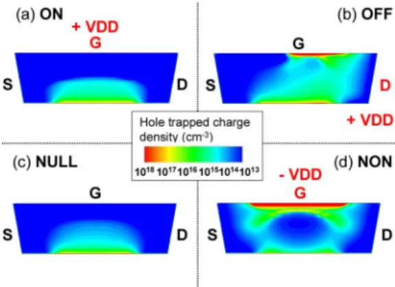
The shape of the electric-field lines is first calculated as a function of the bias configuration before irradiation. The result of this simulation is displayed in Fig. 10 where the isopoten-tial lines are drawn for the ON-state [Fig. 10(a)], the
NULL-state [Fig. 10(b)], theOFF-state [Fig. 10(c)], and theNON-state
[Fig. 10(d)]. The white arrows perpendicular to the isopotential curves depict the electric field. Fig. 11 shows the resulting radi-ation-induced hole trapping after a total ionizing dose exposure following the same bias conditions during irradi-ation, respectively.
In theON-state [Fig. 10(a)], the electric-field lines originating
from the gate reach directly to the silicon channel/oxide inter-face where the radiation-induced charges can be mostly trapped [Fig. 11(a)]. The electrostatic potential in the silicon is thus effi-ciently modified inducing the threshold voltage shift ob-served in Fig. 9 (over 50 V after ).
In the OFF state [Fig. 10(b)], the electric-field lines leave
the drain to mainly reach either the gate/oxide interface of the silicon/oxide interface. This leads to a high concentration of trapped holes in these areas [Fig. 11(b)], which locally exceeds the one obtained in the ON-state. However, despite the high
Fig. 10. Simulated electrostatic potential in the oxide of the FOXFET in the (a)ON-state, (b) theOFF-state, (c) the NULL-state, and (d)NON-state before ir-radiation. The arrows correspond to the shape of the electric-field lines.
Fig. 11. Simulated radiation-induced hole trapped charge in the 400-nm-thick gate oxide of the FOXFET. Hole-trapped charge profiles are calculated according to the same bias configurations as in Fig. 10.
concentration, the radiation-induced hole trapped charge is not enough evenly distributed along the conduction channel. The surface potential in the silicon is not sufficiently modified to imply a similar voltage shift than the one observed in the
ON-state.
In the NULL-state [Fig. 10(c)], all terminals are grounded during irradiation. Electrostatic potential drops are thus only due to doping gradients. This leads to similar shapes of electric field lines as the one observed in theOFF-state. Only the maximum
value of the electric field is lowered. The radiation-induced hole trapped charges are consequently mainly located at the silicon/ oxide interface but with lower densities [Fig. 11(c)].
Finally, the NON-state [Fig. 10(d)] corresponds to the exact opposite bias case to theON-state. The electric-field lines point
directly to the gate electrode where most of the radiation-in-duced charges are trapped. At the source/bulk and drain/bulk junctions, some electric-field lines also leave the source and drain to reach the bulk silicon due to the potential drops at PN junctions (such as in the NULL-state). This may explain the more complex hole trapped charge profile obtained in this bias case during irradiation [Fig. 11(d)]. Most of the radiation-in-duced trapped holes are located directly at the gate/oxide inter-face far from the silicon/oxide interinter-face. At the beginning of the irradiation, the holes trapped at the silicon/oxide interface are only due to the few electric-field lines originating from the source and drain. For higher total ionizing doses, the effect of
the gate bias is gradually weakened. This is due to the strong buildup of the positive oxide trap charge directly at the gate/ oxide interface supporting the reversal of the electric field in this region. To summarize, most of the radiation-induced trapped holes are far from the silicon/oxide interface, impacting the sur-face potential in the silicon less and then the device electrical characteristics.
C. Discussion on the Effect of Bias on the Buildup of Interface Traps in Trench Oxides
Assuming the hole-trapped charge profiles calculated in Fig. 11, the low external electric field due to the external bias applied on the electrodes during irradiation may be much lower than the one induced by the positive charge buildup in the oxide bulk. The shape of the electric field in the oxide can be sufficiently modified to induce the transport of protons liberated during hole transport to silicon/oxide interfaces where they may generate in-terface traps, even in negative bias conditions during irradiation (NON-state [Fig. 11(d)]. TCAD calculations performed in the
NON-state show such an electric field reversal through the STI at high TID. So, as already proposed in [32], this electric-field modification may support the increase of the contribution re-lated to the interface traps , cancelling the oxide-trapped charges contribution on the apparent threshold voltage shift observed in Fig. 8 (red circles). This point needs to be further investigated to be completely clarified. To do so, experiments using various negative biases should be carried on in addition to postirradiation anneals in order to maximize the relative contribution of the interface traps over the one related to the oxide-trapped charges.
V. TRENDS ON THERINCE INI/O TRANSISTORS
After discussing the properties of the trench oxide via the characterization and modelling of a dedicated structure, the FOXFET, this section now focuses on the effect of the oxide traps in shallow trench isolations on the electrical characteris-tics of typical I/O transistors (using the GO2 option) based on a bulk 0.18 m CMOS process.
A. Trends on the Radiation-Induced Narrow Channel Effects in I/O Transistors
3-D TCAD simulations were performed on an NMOS I/O transistor structure encapsulated in STI with various device widths. Simulations were carried on in theON-state bias
config-uration during irradiation. Based on the results of Section IV-B on the FOXFET and on the shape of the electric-field lines in the STI under a positive bias on the gate electrode, the hole-trapped charge is distributed at the STI/silicon interface along the conduction channel. Furthermore, trapped charges are spread in the entire thickness of the STI down to the bottom of the source and drain regions. The same simulation would have been performed in theNON-state using a trapped charge
distribution always evenly distributed along the conduction channel but mainly located in the upper part of the STI (e.g., at the gate-STI-silicon corner). Since the hole-trapped charge in the STI does not depend on the width of the transistor, the same amount of charge is applied at the STI/silicon interfaces whatever the width of the simulated transistor is.
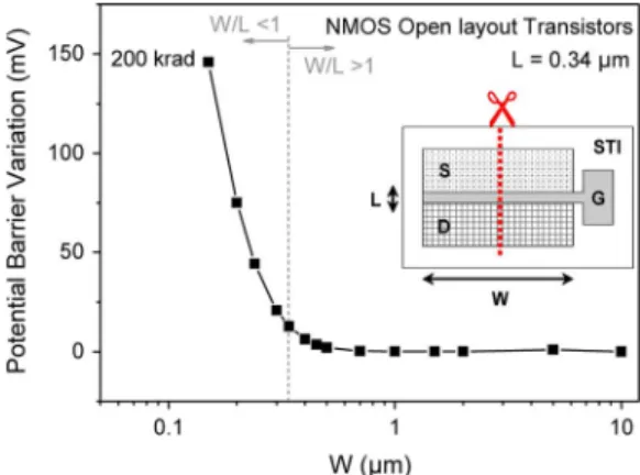
Fig. 12. Simulated source-channel potential barrier variation in the silicon, at the silicon/gate–oxide interface, in the source-drain axis. The curves are probed in the middle of the transistor width which varies from 0.15 m 0.44 to 10 m 30 . The gate length is fixed at 0.34 m. A sheet density of charges corresponding to a 200 irradiation is applied at the STI/ silicon interface in each case.
Fig. 12 exhibits the simulated source-to-channel potential barrier drop in the middle of the transistor width. This param-eter is extracted for several transistors’ width giving a picture of the RINCE. Potential barriers are probed at the exact same distance of both lateral STIs. This corresponds to the minimum electrostatic potential variation in the conduction channel area induced by the trapped charges in the STI. The potential barrier drop will be larger when probing it closer to the silicon/STI interface.
In wide transistors , trapped holes at the STI/sil-icon interfaces can efficiently modify the electrostatic potential only in the area where they are trapped, inducing the STI side-wall leakage current in NMOS transistors. However, they do not have a sufficient “range of action” to degrade the potential well in the whole width of the transistor. The source-to-drain potential barrier height in the middle of the transistor width re-mains sufficiently high to avoid any threshold voltage shift of the main transistor as observed in Fig. 2(a). However, the par-asitic conduction at the edges of the transistor remains active with increasing TID (not shown here).
In narrow transistors , the radiation-induced pos-itive trapped charges in the STI strongly lower the source-to-drain potential barrier in the active silicon even in the middle of the transistor’s width. The STI trapped charges induce a low-ering of the potential barrier in the entire width of the transistor. In other words, the narrow transistor may be modelled as a se-ries of only few discrete elementary transistors in parallel across the gate width (by contrast, the wide transistor may be mod-elled using a series of a large number of such discrete elemen-tary transistors). Thus, the trapped charge in the STI is sufficient to induce an efficient potential drop in all of these elementary transistors. So the main transistor which is modelled by the sum of each discrete elementary transistor is thus strongly affected by this potential drop which results in the threshold voltage shift observed in Figs. 2(b) and 4. Conversely, for the wide channel case, the potential drop does not extend across the entire gate width, less impacting the device response. Similar interpreta-tions can be made for PMOS transistors. They only play a role on parasitic sidewall conduction. Here, however, it is shifted far
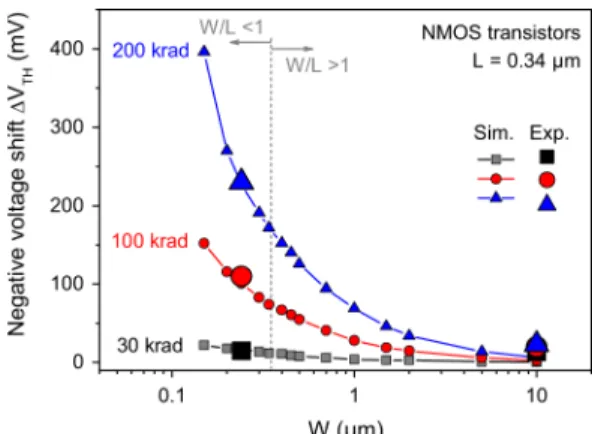
Fig. 13. Simulated threshold voltage shift on NMOS transistors as a function of the transistor geometry expressed as the transistor’s width. Results are shown for three levels of total ionizing dose: 30 krad (black squares), 100 krad (red circles), and 200 krad (blue triangles). Experi-mental data are added by using large symbols.
from the main PMOS transistor without significantly changing its electrical characteristic.
In contrast, as already observed in NMOS transistors, the re-duction of the transistor width enhances the effect of the trapped charge in the STI on the electrostatic potential in the entire width of the transistor. Furthermore, the contribution of the positively charged interface traps strengthens the threshold voltage shift instead of limiting it in NMOS transistors explaining the large RINCE depicted in Figs. 5 and 6.
B. Implications for Circuit Design for Radiation Hardening of ICs Based on COTS Technology
For each simulated transistor, the threshold voltage shifts induced by the positive charges trapped at the STI/silicon interface were extracted to gain additional insights on the ionizing radiation sensitivity of such transistors related to their geometries. Calculated results are summarized in Fig. 13 as a function of the transistor’s width W at various levels of positive charge densities (e.g., total ionizing dose) Simulations are compared to experimental results (added using large symbols). Fig. 13 reveals good agreement between simu-lations and experiments.
In Fig. 13, the gate length is fixed at the nominal value for I/O transistors of this technology 0.34 m. The transistor width W is thus the sole variable parameter. We choose to indicate the corresponding W/L ratio in order to keep in mind that analog circuit designers generally avoid using the W/L ratio smaller than one. However, specific applications, such as CMOS image sensors, need smaller W/L ratios to improve the integration of the electronic part close to the photodetection part.
This graph exhibits a clear trend on the radiation-induced narrow channel effect as a function of the transistor geometry. The smaller the transistor’s width, the higher the transistor sen-sitivity to ionizing radiation is. Such a trend is very close for PMOS transistors. Core transistors (GO1) from the same tech-nology are most probably not as sensitive as transistors designed using the GO2 option of the technology. Since core transistors use an extremely thin gate oxide, the gate electrode has a much
stronger capacitive control of the electrical potential over the conduction channel. But depending on the doping concentration in the channel region and on the transistor’s design, a RINCE may also be observed and it needs further investigation to be ex-tensively quantified. However, GO2 transistors are widely used for analog applications, I/Os, and optoelectronic devices, such as CMOS image sensors. In the worst case, this set of data shows that the RINCE may imply significant threshold voltage shifts for relatively low TID (about 150 mV at 100 krad, and about 400 mV at 200 krad), both on NMOS and PMOS transistors. This should be taken into account to manage a hardening strategy to design radiation-tolerant circuits based on COTS technology within the requirements of the intended radiative environment. Furthermore, these values of threshold voltage shifts may be easily introduced in circuit simulations to predict the sensitivity to ionizing radiation of elementary cells. This approach would help one to adjust the mitigation strategies for the radiation hard-ening by the design of ICs.
VI. CONCLUSION
We demonstrate that charge trapping in trench oxides induces an unexpected enhanced radiation-induced narrow channel ef-fect in bulk transistors used in I/O and analog circuits. A weaker RINCE was already observed in NMOS transistors by [11]. However, strong unexpected modifications of PMOS transistors’ characteristics are exhibited. They may compro-mise circuit hardening if this phenomenon is neglected in the radiation hardening by design strategy. Investigations on the charge-trapping properties of shallow trench isolations using the FOXFET are discussed by using experiments along with dedicated self-consistent calculations of charge trapping in oxides. The dependence of the voltage shifts with the bias configuration used during irradiation is discussed related to the oxide-trapped charge and to the interface traps. Insights into the effect of the charge-trapping location on the electrostatic potential modifications induced inside the active silicon are reported. From these data obtained on the trench oxide, 3-D TCAD simulations were then performed on nominal transis-tors to understand the physical mechanisms leading to the enhanced radiation-induced narrow channel effect as evidenced on experiments. Finally, calculations were conducted to draw trends on the radiation sensitivity of elementary devices as a function of their geometries to discuss the radiation hardening by design issues on GO2 transistors optimized for analog, I/O, and optoelectronic applications.
REFERENCES
[1] P. Paillet, M. Gaillardin, V. Ferlet-Cavrois, A. Torres, O. Faynot, C. Jahan, L. Tosti, and S. Cristoloveanu, “Total ionizing dose effects on deca-nanometer fully depleted SOI devices,” IEEE Trans. Nucl. Sci., vol. 52, no. 6, pt. 1, p. 2345, Dec. 2005.
[2] M. Gaillardin, P. Paillet, V. Ferlet-Cavrois, O. Faynot, C. Jahan, and S. Cristoloveanu, “Total ionizing dose effects on triple-gate FETs,” IEEE
Trans. Nucl. Sci., vol. 53, no. 6, pt. 1, pp. 3158–3165, Dec. 2006.
[3] M. Gaillardin, P. Paillet, V. Ferlet-Cavrois, S. Cristoloveanu, O. Faynot, and C. Jahan, “High tolerance to total ionizing dose of omega-shaped gate field-effect transistors,” Appl. Phys. Lett., vol. 88, no. 22, p. 223511, 2006.
[4] F. E. Mamouni, E. X. Zhang, R. D. Schrimpf, D. M. Fleetwood, R. A. Reed, S. Cristoloveanu, and W. Z. Xiong, “Fin-width dependence of ionizing radiation-induced subthreshold-swing degradation in 100-nm-Gate-Length FinFETs,” IEEE Trans. Nucl. Sci., vol. 56, no. 6, pp. 3250–3255, Dec. 2009.
[5] M. Bagatin, G. Cellere, S. Gerardin, A. Paccagnella, A. Visconti, and S. Beltrami, “TID sensitivity of NAND flash memory building blocks,”
IEEE Trans. Nucl. Sci., vol. 56, no. 4, pt. 2, pp. 1909–1913, 2009.
[6] M. Bagatin, S. Gerardin, G. Cellere, A. Paccagnella, A. Visconti, N. Bonanomi, and S. Beltrami, “Error instability in floating gate flash memories exposed to TID,” IEEE Trans. Nucl. Sci, vol. 56, no. 6, pp. 3267–3273, Dec. 2009.
[7] F. E. Mamouni, M. Bawedin, E. X. Zhang, R. D. Schrimpf, D. M. Fleet-wood, and S. Cristoloveanu, “Total dose effects on the performance of irradiated capacitorless MSDRAM cells,” IEEE Trans. Nucl. Sci., vol. 57, no. 6, pt. 1, pp. 3054–3059, 2010.
[8] M. R. Shaneyfelt, J. R. Schwank, D. M. Fleetwood, and P. S. Winokur, “Effects of irradiation temperature on MOS radiation response,” IEEE
Trans. Nucl. Sci, vol. 45, no. 3, pp. 1372–1378, Jun. 1998.
[9] H. J. Barnaby, “Total-ionizing-dose effects in modern CMOS technolo-gies,” IEEE Trans. Nucl. Sci., vol. 53, no. 6, p. 3103, 2006.
[10] M. Turowski, A. Raman, and R. D. Schrimpf, “Nonuniform total-dose-Induced charge distribution in shallow-trench isolation oxides,” IEEE
Trans. Nucl. Sci., vol. 51, no. 6, pp. 3166–3171, Dec. 2004.
[11] F. Faccio and G. Cervelli, “Radiation-induced edge effects in deep sub-micron CMOS transistors,” IEEE Trans. Nucl. Sci, vol. 52, no. 6, pp. 2413–2420, Dec. 2005.
[12] R. C. Lacoe, J. V. Osborn, D. C. Mayer, S. C. Witczak, S. Brown, R. Robertson, and D. R. Hunt, “Total-dose tolerance of a chartered semiconductor 0.35- CMOS process,” in Proc. Radia., Effects Data
Workshop, 1999, p. 82.
[13] R. C. Lacoe, J. V. Osborn, R. Koga, S. Brown, and D. C. Mayer, “Application of hardness-by-design methodology to radiation-tolerant ASIC technologies,” IEEE Trans. Nucl. Sci., vol. 47, no. 6, pp. 2334–2341, Dec. 2000.
[14] A. H. Johnston, R. T. Swimm, and T. F. Miyahira, “Low dose rate effects in shallow trench isolation regions,” IEEE Trans. Nucl. Sci., vol. 57, no. 6, pt. 1, pp. 3279–3287, 2010.
[15] M. McLain, H. J. Barnaby, K. E. Holbert, R. D. Schrimpf, H. Shah, A. Amort, M. Baze, and J. Wert, “Enhanced TID susceptibility in sub-100 nm bulk CMOS I/O transistors and circuits,” IEEE Trans. Nucl. Sci., vol. 54, no. 6, pt. 1, pp. 2210–2217, Dec. 2007.
[16] V. Goiffon, M. Estribeau, and P. Magnan, “Overview of ionizing ra-diation effects in image sensors fabricated in a deep-submicrometer CMOS imaging technology,” IEEE Trans. Electron. Dev., vol. 56, no. 11, pp. 2594–2601, Nov. 2009.
[17] J. R. Schwank, Total dose effects in MOS devices. Phoenix, AZ: NSREC Short Course, 2002.
[18] P. J. McWhorter and P. S. Winokur, “Simple technique for separating the effects of interface traps and trapped-oxide charge in metal-oxide-semiconductor transistors,” Appl. Phys. Lett., vol. 48, no. 2, p. 133, 1986.
[19] D. M. Fleetwood, P. S. Winokur, C. M. Dozier, and D. B. Brown, “Ef-fect of bias on the response of metal-oxide-semiconductor devices to low-energy x-rays and cobalt-60 irradiation,” Appl. Phys. Lett., vol. 52, no. 18, p. 1514, 1988.
[20] D. M. Fleetwood, P. S. Winokur, R. A. Reber, T. L. Meisenheimer, J. R. Schwank, M. R. Shaneyfelt, and L. C. Riewe, “Effects of oxide traps, interface traps, and border traps metal-oxide-semiconductor devices,”
J. Appl. Phys, vol. 73, no. 10, p. 5058, 1993.
[21] D. M. Fleetwood, M. R. Shaneyfelt, and J. R. Schwank, “Estimating oxide-trap, interface-trap, and border-trap charge densities in metal-oxide-semiconductor transistors,” Appl. Phys. Lett., vol. 64, no. 15, p. 1965, 1994.
[22] R. Pease, D. Emily, and H. E. Boesch, “Total dose induced hole trap-ping and interface state generation in bipolar recessed field oxides,”
IEEE Trans. Nucl. Sci., vol. NS-32, no. 6, pp. 3946–3952, Dec. 1985.
[23] H. E. Boesch and T. L. Taylor, “Charge and interface state generation in field oxides,” IEEE Trans. Nucl. Sci., vol. NS-31, no. 6, pp. 1273–1279, Dec. 1984.
[24] P. S. Winokur, J. M. McGarrity, and H. E. Boesch, “Dependence of interface-state buildup on hole generation and transport in irradiated MOS capacitors,” IEEE Trans. Nucl. Sci., vol. NS-23, no. 6, pp. 1580–1585, Dec. 1976.
[25] H. E. Boesch, F. B. McLean, J. M. Benedetto, J. M. McGarrity, and W. E. Bailey, “Saturation of threshold voltage shift in mosfet’s at high total dose,” IEEE Trans. Nucl. Sci., vol. NS-33, no. 6, pt. 1, pp. 1191–1197, Dec. 1986.
[26] H. J. Barnaby, M. L. McLain, I. S. Esqueda, and X. J. Chen, “Modeling ionizing radiation effects in solid state materials and CMOS devices,”
IEEE Circuits Syst. I, Reg. Papers, vol. 56, no. 8, pp. 1870–1883, Aug.
2009.
[27] H. E. Boesch, “Interface-state generation in thick SiO2 layers,” IEEE
Trans. Nucl. Sci., vol. NS-29, no. 6, pp. 1445–1451, Dec. 1982.
[28] P. S. Winokur, H. E. Boesch, J. M. McGarrity, and F. B. McLean, “Field- and time-dependent radiation effects at the SiO2/Si interface of hardened MOS capacitors,” IEEE Trans. Nucl. Sci., vol. NS-24, no. 6, pp. 2113–2118, Dec. 1977.
[29] P. M. Lenahan and P. V. Dressendorfer, “Effect of bias on radiation-induced paramagnetic defects at the silicon-silicon dioxide interface,”
Appl. Phys. Lett., vol. 41, no. 6, p. 542, 1982.
[30] J. R. Schwank, P. S. Winokur, F. W. Sexton, D. M. Fleetwood, J. H. Perry, P. V. Dressendorfer, D. T. Sanders, and D. C. Turpin, “Radia-tion-induced interface-state generation in MOS devices,” IEEE Trans.
Nucl. Sci., vol. NS-33, no. 6, pp. 1177–1184, Dec. 1986.
[31] M. R. Shaneyfelt, J. R. Schwank, D. M. Fleetwood, P. S. Winokur, K. L. Hughes, and F. W. Sexton, “Field dependence of interface-trap buildup in polysilicon and metal gate MOS devices,” IEEE Trans. Nucl. Sci., vol. 37, no. 6, pp. 1632–1640, Dec. 1990.
[32] D. M. Fleetwood, “Radiation-induced charge neutralization and in-terface-trap buildup in metal-oxide-semiconductor devices,” J. Appl.
Phys., vol. 67, no. 1, p. 580, 1990.