This is an author-deposited version published in: http://oatao.univ-toulouse.fr/ Eprints ID: 10211
To link to this article: DOI: 10.1364/AO.52.000C16
URL: http://dx.doi.org/10.1364/AO.52.000C16
To cite this version: Rolando, Sébastien and Goiffon, Vincent and Magnan, Pierre and Corbière, Franck and Molina, Romain and Tulet, Michel and Bréart-de-Boisanger, Michel and Saint-Pé, Olivier and Guiry, Saïprasad and Larnaudie, Franck and Leone, Bruno and Perez-Cuevas, Leticia and Zayer, Igor Smart CMOS image sensor for lightning detection and imaging. (2013) Applied Optics, vol. 52 (n° 7). pp. C16-C23. ISSN 0003-6935
O
pen
A
rchive
T
oulouse
A
rchive
O
uverte (
OATAO
)
OATAO is an open access repository that collects the work of Toulouse researchers and makes it freely available over the web where possible.
Any correspondence concerning this service should be sent to the repository administrator: [email protected]
Smart CMOS Image Sensor for Lightning Detection and
Imaging
Sébastien Rolando,1,* Vincent Goiffon,1 Pierre Magnan,1 Franck Corbière,1 Romain Molina,1 Michel Tulet,2 Michel Bréart-de-Boisanger,2 Olivier Saint-Pé,2 Saïprasad Guiry,2
Franck Larnaudie,2 Bruno Leone,3 Leticia Perez-Cuevas,3 and Igor Zayer3
1
ISAE, Université de Toulouse, Image Sensor Research Team, 10 Avenue E. Belin, 31055 Toulouse, France
2
EADS Astrium, 31 Avenue des cosmonautes, 31402 Toulouse, France 3
European Space Agency, ESTEC, Kerplerlaan 1, 2201 AZ Noordwijk, The Netherlands *
Corresponding author: [email protected]
We present a CMOS image sensor dedicated to lightning detection and imaging. The detector has been designed to evaluate the potentiality of an on-chip lightning detection solution based on a smart sensor. This evaluation is performed in the frame of the pre-development phase of the lightning detector that will be implemented in the Meteosat Third Generation Imager (MTG-I) satellite for European Space Agency (ESA). The lightning detection process is performed by a smart detector combining an in-pixel frame-to-frame difference comparison with an adjustable threshold and on-chip digital processing allowing an efficient localization of a faint lightning pulse on the entire large format array at a frequency of 1 kHz. A CMOS prototype sensor with a 256x256 pixel array and a 60 µm pixel pitch has been fabricated using a 0.35 µm 2P 5M technology and tested to validate the selected detection approach.
1 Introduction
Lightning detection and imaging from the earth orbit is a very important tool for real time monitoring of thunderstorm activities [1]. It also brings very useful data to assess the impact of the climate change. Moreover lightning monitoring is necessary to study the processes at the origin of harmful nitrogen oxides in the atmosphere. Ground-based detectors have a limited detection range leading to a poor coverage of ocean and low population areas. Earth observation satellites allow a long term stable and spatially homogeneous observation of the lightning activity, as demonstrated by the National Aeronautics and Space Administration (NASA) Optical Transient Detector (OTD) and Lightning Imaging Sensor (LIS) instruments in low earth orbit [2].
The Lightning Imager (LI) instrument of the European Space Agency (ESA) Meteosat Third Generation Imager satellite (MTG-I) will be dedicated to the monitoring of Earth atmosphere lightnings for meteorological studies and forecast from a geostationary orbit. In addition to both National Oceanic and Atmospheric Administration (NOAA) Geostationary Lightning Mapper (GLM [3]), the instrument will contribute to near global earth coverage. Table 1 presents the main specifications of these lightning activity observation instruments.
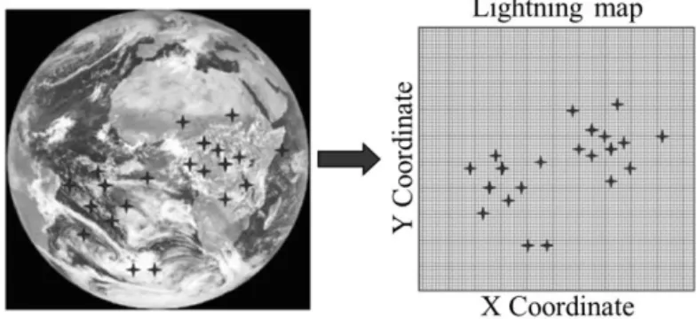
The LI [4] will continuously observe over 80 % of the Earth disk and will provide a real time lightning detection and geo-localization (Fig. 1). Contrary to the GLM instruments that use high speed Charge Coupled Devices (CCD), the LI is based on a CMOS Image Sensor (CIS) for detection, localization and measurement of lightning events. The scene background is temporally and spatially non-uniform and can be much higher than the useful signal [5].
Table 1. Specifications of lightning activity observation instruments.
Sensor Type Array size (pixels) Ground sampling distance Orbit Integration time Detection efficiency* Year OTD CCD 128 x 128 10 km 710 km 2 ms >50% 1995 - 2000 LIS CCD 128 x 128 4-7 km 350 km 2 ms 90% 1997 - Present GLM CCD 1372 x 1300 8-14 km 31000 km 2 ms 70% - 90% Future * after on-board post-processing
Fig. 1. The lightning detector instrument will continuously observe over 80% of the Earth disk and will provide a real time lightning detection and geo-localization.
The most straightforward way to achieve the LI mission goal is to readout all the pixel values at the frame frequency and to determine the events localization and energy thanks to off-chip post processing. However, the targeted high frame rate (1 kilo-frame per second) associated to the small number of expected lightnings per frame lead to a huge detector data output flow (over 1 Gpixels/s) and a large resource consumption that are unnecessary. A smart sensor [6-8] with in-pixel detection was chosen because only the relevant information (lightning characteristics) is transmitted off-chip in this case, leading to a great reduction of data flow and consumption [9].
In this paper we present the circuit design and the characterization results of the CIS developed during the pre-development phase of the LI instrument. The main objective of this study is to evaluate the potentiality of an on-chip lightning detection solution based on a smart sensor design. Such architectural evaluation can be performed independently of the detector radiometric performances which are mainly given by technological choices (by opposition to architectural choice). Therefore, the demonstrator has been implemented in standard 0.35 µm CMOS technology (non-optimized image sensor technology) leading to a Front-Side Illuminated CIS, with no micro-lense and no coating or doping profile optimized to improve sensitivity.
This demonstrator allows a permanent observation on a focused scene at 1 kHz and the identification (ground location and time tapping) of optical events overstepping a controlled
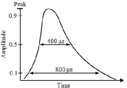
threshold corresponding to the event energy to be detected whatever the nature of the background. It measures also the intensity of these triggered events (TE) and the background value. The assumed [10] lightning optical pulse characteristics illustrated in Fig. 2 have 10 km diameter, 800 µs constant duration, with a total energy in the range 4 µJ.m-2.sr-1 to 400 µJ.m-2.sr-1 at 777.4 nm (oxygen line at 760 nm). These optical pulses are superimposed to a background that can reach 0.6 W.m-2.sr-1 at instrument input. The equivalent numbers of photo-generated electrons in each pixel with an optical pulse which can satisfy the instrument requirements are 1450 e- for the minimum flash and 130 ke- for the maximum flash with a maximum background value of 100 ke-. The demonstrator and mission requirements are reported in Table 2.
Fig. 2. Lightning flash shape. The entire lightning energy is emitted within a 2 ms interval.
Table 2. Demonstrator and mission requirements
Requirement Value
Demonstrator Goal
Array size 256 x 256 1024 x 1024
Pixel pitch 60 µm ≤ 50 µm
Wavelength 777.4 nm
Flash energy range 4 µJ.m-2.sr-1 to 400 µJ.m-2.sr-1
Lightning detection probability (in each frame) > 90 % For a flash of 7 µJ.m-2.sr-1 > 50 % For a flash of 4 µJ.m-2.sr-1
False alarm probability (in each frame)
< 2 sec-1 < 1 sec-1
Lightning Energy and Background measurement accuracy 20 % 10 % Maximum rate of lightning events 400 sec-1 500 sec-1 Spatial resolution of detected Lightning event
Circular flash with 10 km diameter
Ground Sampling Distance (GSD)
4 km (always 2 pixels hit by flash)
Integration time 1 ms
2 Architecture and operation principle
Fig. 3 shows the architecture of the proposed CMOS image sensor [11]. The image sensor consists of an array of “smart” pixels (able to detect and measure the lightning events), the TE
processing function that provides the detection and the localization of an optical pulse (i.e. triggered event), the RAD function that provides the radiometric value measurement and the row sequencer that generates the pixel commands.
Fig. 3. Demonstrator block diagram. The detector is constituted of two main parts: the Triggered Event (TE) processing functions that provide the detection and the localization of an optical pulse and the Radiometric (RAD)
functions that provide the radiometric value measurement.
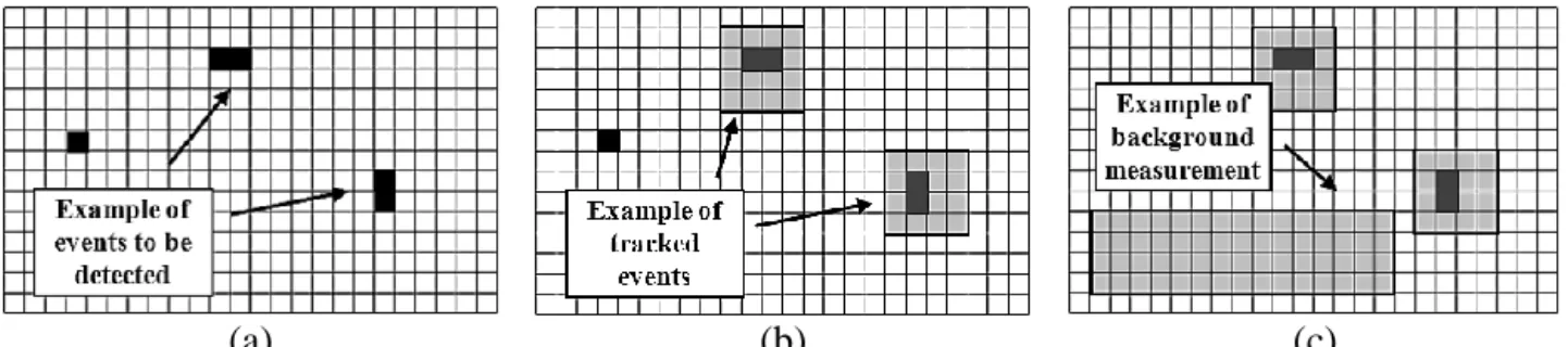
The detector performs simultaneously three tasks. The first task, based on a continuous scan of the pixel array, is to detect the events which means the triggering of the pixels for which transient event signal is higher than an adjustable threshold and then to send the addresses of triggered cells to off-chip electronics (Fig. 4.a). The second task is to measure the signal levels of the triggered pixels (Fig. 4.b). The readout of a triggered pixel includes also the readout of surrounding pixels which constitute the Area Of Interest (AOI). And the third task is to measure the signal levels of the pixels for the continuous measurement and the averaging of background image radiance (Fig. 4.c). The operation principle will be explained by describing the pixel and the two detector functions RAD and TE more in detail.
(a) (b) (c)
Fig. 4. The three simultaneous tasks of the demonstrator. (a) Detection of events. (b) Readout of event radiometric values that pass the filters of reduction of false alarms and the AOI (random access). (c) Background measurement
A. Pixel description
The lightning detection is realized at pixel level and the principle is based on a frame-to-frame difference comparison with a threshold. The in-pixel frame-to-frame difference [12,13] was selected because it allows the cancelation of the slowly varying signal pedestal corresponding to the scene background. It also allows lightning detection whatever the nature of the scene. The pixel operates as follows: at each frame, the voltage corresponding to the radiometric measurement of this frame is subtracted from the value of the previous one. The result corresponding to the scene intensity variation is compared to a global threshold that corresponds to a minimal lightning energy. If the result of the frame-to-frame difference is higher than the threshold, the intensity variation is defined like an event and the TE output flag is set to ‘1’. The threshold reference voltage is used to adjust the comparator threshold (to optimize the detection efficiency) and to compensate the detection circuit offset.
The overview of the pixel processing functions is presented in Fig. 5. It is constituted by Nwell/P photodiode, a sample and hold circuit for the storage of the radiometric measurement that allows the RAD readout during the next frame, a differentiator subtracting two successive radiometric acquisitions, a comparator comparing the frame-to-frame difference output to the global threshold reference voltage (VTH) and two switches to enable output values for the RAD
and TE functions. The outputs of the pixel are the TE digital state that indicates the event detection and an analog output corresponding to the radiometric measurement.
Fig. 5. Pixel processing functions.
The circuits used in the pixels have been selected after a comparative study between several architectures. The selected solution for the sample and hold circuit is to use one path to the subtraction operator instead a two path solution with two sample and hold circuits for the N and N-1 frame. The single path solution degrades less the pixel fill factor with only one sampling capacitor and it offers a very efficient offset cancellation with the same path for all frames (offset mismatches between the paths is not an issue here since there is only one path).
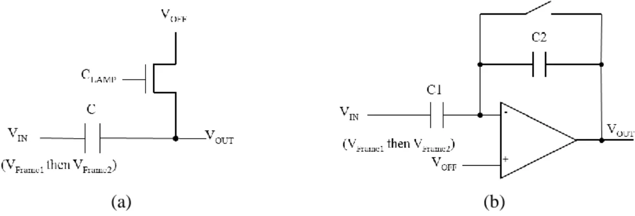
The frame-to-frame difference operator should use only one input path to be compliant with the selected sample and hold function. Two main architectures were studied (Fig. 6): clamp circuit and switched capacitor amplifier (with and without offset cancellation). The most critical parameters of the frame-to-frame difference function are the offset mismatches because the output value is compared to a global threshold (i.e. by pixel threshold adjustment implies the use
of in-pixel analog memory that would degrade too much the pixel fill factor). If these voltage variations are large, pixels may continuously be triggered (permanent false alarms). The clamp performances preserve the detection efficiency and they comply with the specifications. It is a simple solution with small dimensions but the output signal is not amplified. Hence the reference voltage is not supposed to be not sensitive to parasitic coupling and offset mismatches of the comparator (the minimum voltage signal corresponding to the minimum flash variation is close to 10 mV at photodiode level). It is for these reasons that we decided to use a switched-capacitor amplifier to realize the frame-to-frame difference because it allows to have a significant amplification on the result of the frame difference. A switched-amplifier with an offset cancellation offers better results but it doesn’t improve significantly the detection efficiency when the gain is superior to 10. To optimize the pixel fill factor, a switched-capacitor amplifier without offset cancellation was selected.
(a) (b)
Fig. 6. Frame-to-frame difference operator: (a) Clamp circuit and (b) switched-capacitor amplifier.
Thanks to the amplification of the frame-to-frame difference result, a comparator without offset cancellation is used because mismatch issues are less critical. The final pixel architecture is presented in Fig. 7. The pixel pitch is 60 µm with 70 % of fill factor and is constituted of 42 transistors and 2 capacitors (Fig. 8).
Fig. 8. Detailed layout of pixel.
B. TE management system
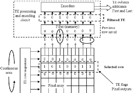
Fig. 9 presents the TE management system. It is constituted by two peripherals circuits in addition to the part dedicated to the lightning detection in pixels. First the TE row sequencer that performs the selection of row of TE flags in rolling mode (scanning frequency at 1 kHz). All the TE flags are read during each frame. And secondly, the TE processing and encoding circuit that performs the first stage of signal processing to filter false alarms and encodes the TE addresses.
Fig. 9. TE management functions. This system part is used to localize in rolling readout mode the first and the last TE on each row of the pixel array.
The challenge for the TE encoding circuit is to define a fast and efficient algorithm to identify the TE addresses. The TE encoding circuit input is a binary word where a bit at ‘1’ corresponds to an identified event by one pixel on the selected line (by the TE row sequencer). This word can contain several active flags but their number is assumed to be very low because the maximum rate of lightning events by frame is low (400 lightning/s with 1000 frame/s). The size of this binary word is equal to the number of columns of the pixel array (close to 1000 bits
for the final instrument). To realize the management of detected events, the encoding of the addresses of the first and last active flag in the row was chosen. This solution uses only logic combinatory that allows encoding TE addresses at the row frequency. Two encoders are used to perform simultaneously the encoding of these two TE addresses. The circuit outputs are two binary words corresponding to these two addresses.
Before encoding the event addresses, a spatial filtering is applied on TE flags to reduce the number of false alarms. With a ground sampling distance (GDS) of 4 km and a spatial resolution of detected lightning event of 10 km, each lightning event must impact at least two neighbor pixels. So, the filter allows suppressing all events that have affected an isolated pixel (i.e.
transient perturbations induced by noisy pixels or by some space particles). For this, the TE flags of two consecutive rows are stored in the filter memory then a simple Boolean equation is
applied between contiguous TE flags. The filter is entirely configurable and each pair of TE flags can be activated individually. The Fig. 10 illustrates the operation of TE filter.
The TE management system outputs are the first and the last address of filtered TE of each row and a flag that indicates that there is a valid TE address on the outputs.
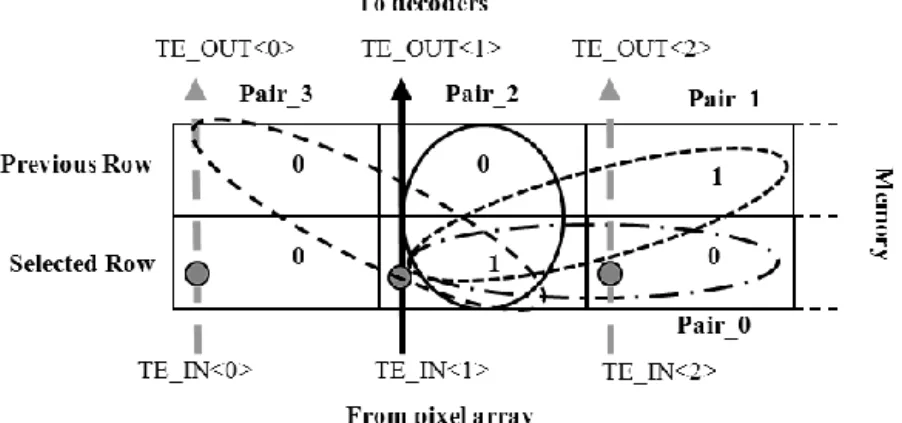
Fig. 10. Spatial filter applied to TE flags. In this example, two TE flags are activated in Pair_1. So, the TE_OUT<1> is set to high. If no pair contains two active flags the TE_OUT<0> stay to low. This filter is identical for all TE_IN.
C. Rad readout circuit
Fig. 11 presents the detail of RAD readout system. It is based on a standard readout circuit of a CMOS image sensor with decoders for pixel addressing [7]. The main difference is the simultaneous sampling of four consecutive pixel rows corresponding to the size of the AOI window surrounding a pixel that has detected an event (Fig. 4.b). This feature maximizes the number of tracking windows corresponding to the number of events that can be read in one frame by reducing the time required to read one window (only one column sampling time for one AOI instead of four). This way, one address on the RAD row decoder activates simultaneously four rows. The RAD values of these selected rows are sampled on the column sampling circuits and are multiplexed on the same output signal thanks to the column decoder.
The readout of the 1024 column sampling circuits (1024 circuits because four rows are read simultaneously) on the same output path does not fit with required maximum readout frequency. To deal with the speed requirement without multiplying the number of outputs, the total junction capacitance of the switch transistor loaded by the final output stage is divided by four. Each output stage loads 256 switch drain capacitances instead of 1024 and improves the readout speed. The two most significant bits of RAD column address (X_RAD) are used to multiplex these four analog video outputs.
Fig. 11. RAD readout circuit overview. To maximize the number of tracking windows, four pixel rows which correspond to the size of the AOI window surrounding a pixel that has detected an event are simultaneously sampled
in the column readout circuit.
3 Experimental results
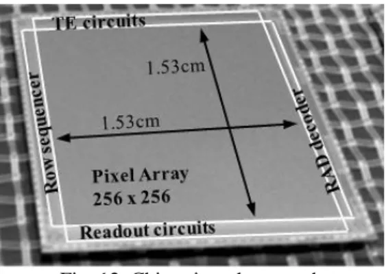
The demonstrator was designed with a standard 0.35 µm 2P 5M process featuring stitching capability for the final instrument. The chip microphotograph of the fabricated chip is shown in Fig. 12. The image array has 256 x 256 pixels with 60 µm pitch. The chip area is 17.8 x 17.8 mm² which includes bond pads.
Fig. 12. Chip microphotograph
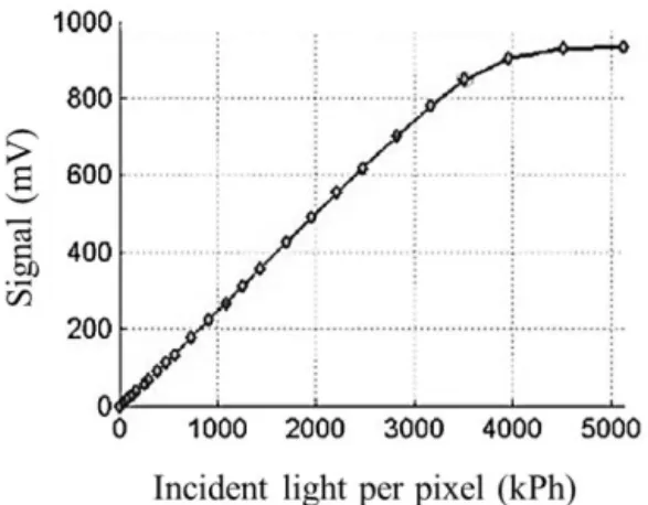
Two sets of measurements have been performed to validate the functionality and the performances of the demonstrator. Firstly, a classical imaging mode characterization that allows validating the functionality of the RAD operation by measuring the supply currents, readout noise and radiometric transfer function (as reported in Table 3). The Fig. 13 shows a sample image taken by the sensor and the Fig. 14 presents its photon transfer curve. Both figures
demonstrate the functionality of the RAD circuit (including the first stage of the TE function: the sample and hold circuit).
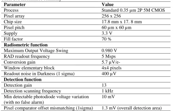
Table 3. Performance summary
Parameter Value
Process Standard 0.35 µm 2P 5M CMOS Pixel array 256 x 256 Chip size 17.8 mm x 17. 8 mm Pixel pitch 60 µm x 60 µm Supply 3.3 V Fill factor 70 % Radiometric function
Maximum Output Voltage Swing 0.980 V RAD readout frequency 5 Msps Conversion gain 5.7 µV/e- Window elementary block 4x4 pixels Readout noise in Darkness (1 sigma) 400 µV
Detection function
Detection gain 13
Detection scanning frequency 1 kHz Min detectable photodiode voltage variation
(with no false alarm)
10 mV
Pixel comparator offset mismatching (1sigma) 1.3 mV (overall detection area)
Fig. 14. Photon transfer curve of demonstrator.
Secondly, the detection mode has been characterized to evaluate the performances of the TE management system (see Table 3 for a performance summary). The spatial filtering functionalities and the TE detection has been charaterized through optical tests, using pulsed LED synchronized with the image timing diagram, where LED beam is focused on 2x2 pixels. The first / last encoding functionalities have been validated with a similar approach except that the LED beam covered 32 columns of the entire pixel array (see Fig. 15). When there is no beam focused on the pixel array no TE flag is activated as shown in Fig. 15.a. On the other hand, when the pulsed LED is used (Fig. 15.b), the beam edge is well detected as illustrated by the activated TE flags that indicate the first and the last events in each row. The comparison performances are presented in Fig. 16. The standard deviation of the computed TE offset (referred to the comparator input in Fig. 7) is about 17 mV (Fig. 16.b). When divided by the average pixel detection chain gain of 13 (Fig. 16.a) it leads to a comparator offset standard deviation referred to the input of the detection chain (photodiode cathode) of approximately 1.3 mV. The Fig. 17 presents the TE threshold detection spreading. This offset spreading including the differentiator and comparator mismatches allows the detection of 10 mV pulses over a background at the photodiode level in the range of 0 to 500 mV without any false alarm. The detection mode appears to be fully functional and reaches the required performances.
(a) (b)
Fig. 15. The TE management system validation. (a) No LED beam is focused on the pixel array: no TE is identified. (b) A LED beam is focused on 32 columns of the entire pixel array: the beam edge is identified.
(a)
(b)
Fig. 16. Pixel comparator offset mismatching. (a) The average value of the pixel detection gain is 13 with a standard variation of 0.75. (b) The standard variation of the computed TE offset is 17 mV (at 1 sigma).
Fig. 17. TE threshold detection (offsets). This offset allows the detection of 10 mV pulses at the photodiode level over a background whitout false alarm.
4 Conclusion
A candidate lightning imager concept for the Meteosat Third Generation has been developed and characterized. Both imaging and detection modes are fully functional. The switched-capacitor amplifier and comparator offset dispersion were low enough to enable the detection of photodiode voltage as low as 10 mV (even with a 500 mV background). If this solution was to be selected for this application, the next step would be to transpose this validated architecture into a CIS process optimized for the narrow spectral band targeted by the application (which would lead to large improvement of the overall quantum efficiency).
Acknowledgements
This study has been carried on under an ESA contract [5] in the frame of the pre-development phase of the MTG-I Lightning Detector.
Appendixes: Acronyms
AOI: Area of Interest
CCD: Charge Coupled Device CIS: CMOS Image Sensor
CMOS: Complementary Metal Oxide Semiconductor ESA: European Space Agency
GLM: Geostationary Lightning Mapper GSD: Ground Sampling Distance LED: Light-emitting diode LI: Lightning Imager
LIS: Lightning Imaging Sensor
MTG-I: Meteosat Third Generation Imager
NASA: National Aeronautics and Space Administration NOAA: National Oceanic and Atmospheric Administration OTD: Optical Transient Detector
TE: Triggered Event
References
1. H. J. Christian, R. J. Blackeslee and S. J. Goodman, “The detection of Lightning from geostationary orbit”, Journal of Geophisycal Research, vol. 94, pp. 13329-13337, 1989 2. D. J. Boccippio and H. J. Christian, “Optical Detection of Lightning from Space”,
Proceedings of the 11th International Conference on Atmospheric Electricity, pp. 746-749, 1999
3. S.Goodman, R. Blackeslee and W. Koshak, "Geostationary Lightning Mapper for GOES-R and Beyond", Fifth GOES Users’ Conference, New Orleans, LA, United States, January 23-24, 2008
4. MTG mission requirement document, EUM/MTG/SPE/06/0011 v2c, 6.3.3 Lightning imagery mission, 2007
5. Large format APS detectors with on-chip intelligence for lightning imaging SOW = TEC-MME/2007/272/IZ, issue 1, rev0, 22.01.2008
6. J. Leijtens, A.Theuwissen and P. Magnan, “Smart FPA’s : Are They Worth The Effort ?”, Proceedings SPIE 6361, Sensors, Systems, and Next-Generation Satellites X, 636115, 2006 7. A. Moini, “Vision Chips”, Kluwer Academic Publishers, 1999
8. J. Ohta, “Smart CMOS Image Sensors and Applications”, CRC Press Inc, 2007
9. L. Tommasi, G. Basile, A. Romoli and M. Stagi, “Design and Performance of the Lightning Imager for the Meteosat Third Generation”, Proceedings of ESA/CNES ICSO, pp. 60.1-60.6, 2006
10. ESA’s Invitation To Tender, “Large format APS detector with on-chip intelligence for lightning imaging”, AO/1-5572/08/NI/EM
11. E. R. Fossum, “CMOS image sensors: electronic camera-on-a-chip”, IEEE Transactions on Electron Devices, vol. 44, pp. 1689-1698, 1997
12. U. Mallik, M. Clapp, E. Choi, G. Cauwenberghs and R. Etienne-Cummings, “Temporal change threshold detection imager”, IEEE International Solid-State Circuits Conference, Digest of Technical Papers, ISSCC, vol. 1, pp. 362-363, 2005
13. Dongsoo Kim, Zhengming Fu, Joon Hyuk Park and E. Culurciello, “A 1-mW CMOS Temporal-Difference AER Sensor for Wireless Sensor Networks”, IEEE Transactions on Electron Devices, vol. 56, pp. 2586-2593, 2009