REPUBLIQUE ALGERIENNE DEMOCRATIQUE ET POPULAIRE
يــــملعلا ثحبلا و يــــلاــــعلا میلعــــتلا ةرازو
MINISTERE DE L’ENSEIGNEMENT SUPERIEUR ET DE LA RECHERCHE SCIENTIFIQUE
اــــبع تاــــحرف ةــــعماج
س
فیطس
1
UNIVERSITE FERHAT ABBAS - SETIF 1 UFAS (ALGERIE)
THESE
Présentée à la Faculté de Technologie Département d’Électronique Pour l’Obtention du Diplôme de
DOCTORAT 3
èmecycle (LMD)
Domaine : Sciences et Technologies
Filière : Electronique
Option : Électronique et Contrôle Industriel
Par
Hamza FEROURA
Stratégies de Commande des Onduleurs de Courant
Triphasés
Soutenue le: 24 /06 /2018 devant le jury composé de:
Nourredine AMARDJIA Professeur à l’université de Sétif 1 Président
Fateh KRIM Professeur à l’université de Sétif 1 Rapporteur
Adel MELLIT Professeur à l’université de Jijel Examinateur
PEOPLE’S DEMOCRATIC REPUBLIC OF ALGERIA
يــــملعلا ثحبلا و يــــلاــــعلا میلعــــتلا ةرازو
MINISTERY OF HIGHER EDUCATION AND SCIENTIFIC RESEARCH
اــــبع تاــــحرف ةــــعماج
س
–
فیطس
1
UNIVERSITY FERHAT ABBAS - SETIF 1 UFAS (ALGERIA)
THESIS
Presented at the Faculty of Technology Department of Electronics
For the Graduation of
Ph. D. 3
rdCycle (LMD)
Field : Sciences and Technologies
Specialty : Electronics
Option : Electronics and Industrial Control
by
Hamza FEROURA
Control Strategies of Three Phase Current Source
Inverters.
Defended on: 24 /06 /2018 in front of the jury composed of:
Nourredine AMARDJIA Professor at university of Setif 1 President
Fateh KRIM Professor at university of Setif 1 Reporter
Adel MELLIT Professor at university of Jijel Examiner
II
Abstract
Current Source Inverter (CSI) topology is gaining acceptance as a competitive alternative for grid interface of renewable energy systems due to its unique and advantageous features. Merits of CSI over the more popular voltage source inverter (VSI) topology have been elaborated on by a number of researchers. However, there is a lack of quality work in control strategies of CSI topology for both stand-alone and grid connected modes. Therefore this thesis contributes by proposing new voltage control techniques, and power control techniques for stand-alone and grid-connected modes, respectively. Existing voltage control techniques for stand-alone CSI are conventional, and complex. They employ usually modulators and regulation loops which are designed depending on the connected load, this reduces the accuracy and stability of the controllers. For this reason, two direct voltage control methods have been proposed in this work. The proposed methods overcome the aforementioned drawbacks of conventional methods. In the other side, PV grid connected CSI systems available in the literature suffer from many problems such like complexity of control strategies, poor power control, filter resonance, and low efficiency. Therefore, new high-performance control strategies are introduced to get over these problems. The proposed techniques can fulfill all the control objectives of the system, i.e. fast and accurate maximum power point tracking, decoupled control of active and reactive powers exchanged with the grid, low distorted grid currents, unity power factor operation or reactive power injection, depending on grid operator demand, and high efficiency through the use of active damping methods. Moreover, system cost and complexity are reduced, and better performances are reached by the use of a sliding mode observer (SMO) instead of hardware sensors. Simulation results using Matlab/Simulink, experimental results, and real-time (RT) implementation results have been carried out to assess the different control techniques proposed in this thesis.
III
Acknowledgement
First and above all, I praise the almighty ALLAH for granting me the capability to proceed successfully. This thesis would not have been possible without the support of several individuals who in one way or another contributed their valuable assistance in the completion of this work.
I would like to express my utmost gratitude and thanks to my academic supervisor, Pr.Fateh KRIM, who has advised, guided and supported me throughout this research work.
I would like to express my thanks to the examiners committee, Pr. Nourredine AMARDJIA,
Dr. Lahcene ZIÉT, and Pr. Adel MELLIT for their valued time and interests in my thesis.
Special thanks to all the members of our laboratory group (LEPCI), and to all my colleagues.
I am so grateful to Dr. Miguel CASTILLA, and Pr. Luis Garcia DE VICUNA for giving me the opportunity to have a long duration training at their laboratory in Barcelona. My thanks go also to all the laboratory group.
Finally, I would like to acknowledge the financial support of the Algerian ministry of higher education and scientific research that have granted me a long duration training abroad.
IV
Dedications
Dedicated
To my parents;
To my wife;
To my sister and my brothers;
And to my friends.
V
Contents
List of tables ...X List of figures ...XI List of abbreviation ...XV List of symbols ...XVII
Chapter 1: Introduction ...1
1.1 Motivation and background ...1
1.2 Objectives ... 4
1.3 Thesis outline ... 4
References ... 6
Chapter 2: Literature survey ... 8
2.1 Introduction ...8
2.2 Distributed generation systems ...8
2.2.1 Distributed generators ...10
2.2.1.1 Photovoltaic generator ...10
2.3 Inverter topologies ... 11
2.3.1 Voltage source inverters ...13
2.3.1.1 Two-level VSI ...13
2.3.1.2 Multi-level VSI ...13
2.3.2 Current source inverters ...14
2.3.2.1 Auto-sequentially commutated CSI ...14
VI
2.3.2.3 Two-level CSI ...15
2.3.2.4 Multi-level CSI ...16
2.4 Inverters control ...17
2.4.1 CSI modulation techniques ...18
2.4.1.1 Carrier-based PWM ...18
2.4.1.2 Trapezoidal PWM ...20
2.4.1.3 Space vector modulation ...21
2.4.1.4 Selective harmonics elimination ...22
2.5 Literature review of CSI based stand-alone systems ...24
2.6 Literature review of CSI based grid-connected systems ...24
2.7 Conclusion ...26
References ... 27
Chapter 3: Design and modeling of system components ...32
3.1 Introduction ...32
3.2 PV model ...32
3.3 CSI model ...35
3.4 Filter modeling and design ...37
3.4.1 Stand-alone CSI ...37
3.4.2 Grid connected CSI ...37
3.4.2.1 CL filter modelling ...38
3.4.2.2 Design criteria ...40
3.4.2.3 Filter resonance and damping ...40
3.5 Conclusion ...44
VII
Chapter 4: Stand-alone current source inverter ...47
4.1 Introduction ...47
4.2 Finite-set model predictive voltage control (FS-MPVC) ...47
4.2.1 Predictive controller ...48
4.2.1.1 Prediction model ...49
4.2.1.2 Cost function optimization ...50
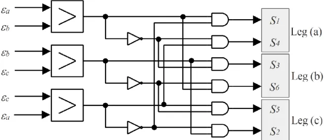
4.3 Proposed CSI switching algorithm ...51
4.3.1 Principle of operation ...52 4.4 Simulation results ...55 4.4.1 Resistive load ...55 4.4.2 Resistive-inductive load ...58 4.4.3 Non-linear load ...59 4.4.4 Robustness tests ...61
4.4.4.1 Sudden load variation ...61
4.4.4.2 Sudden voltage reference variation ...63
4.4.5 Comparative study ...66 4.5 Experimental results ...66 4.5.1 Resistive load ...67 4.5.2 Resistive-inductive load ...68 4.6 Conclusion ...69 References ...70
Chapter 5: Single-stage grid-connected photovoltaic CSI ...71
5.1 Introduction ...71
VIII
5.3 Sliding mode observer (SMO) ...73
5.4 Finite-set model predictive control ...76
5.4.1 FS-MPVC based voltage oriented control (FS-MPVOC) ...76
5.4.1.1 DC-link current control ...77
5.4.1.2 Voltage oriented control (VOC) ...77
5.4.1.3 Proposed active damping method ...79
5.4.1.4 Grid synchronization phase locked loop (PLL) ...80
5.4.2 Finite-set model predictive direct power control (FS-MPDPC) ...80
5.4.2.1 DC-link current control ...81
5.4.2.2 Predictive power controller ...82
5.4.2.3 Proposed active damping method ...84
5.5 Simulation results ...85
5.5.1 SMO performance assessment ...85
5.5.2 Unity power factor operation ...87
5.5.3 Reactive power injection ...94
5.5.4 Comparison between proposed active damping methods and passive jkjnkjnkjnkj...damping ...101
5.6 Real-time implementation results ...75
5.6.1 Unity power factor operation ...103
5.6.1.1 FS-MPVOC ... 103
5.6.1.1 FS-MPDPC ...104
5.6.2 Reactive power injection ...106
5.6.2.1 FS-MPVOC ...106
5.6.2.2 FS-MPDPC ...107
IX
References ...110
Chapter 6: Conclusion ...84
6.1 General conclusion ...84
6.2 Author’s contribution ...85
6.3 Recommendations for future research ...86
Appendix A: Systems’ parameters ...115
Appendix B: Experimental hardware design ...117
X
List of tables
2.1 CSI bi-logic/tri-logic states with corresponding switches triggering signals ...19
2.2 CSI switching states and space vectors ...21
2.3 Comparison of most common CSI modulation techniques ...21
3.1 CSI possible states and corresponding output currents and vectors...36
3.2 Resistive damping configurations ...42
4.1 Comparison between available and proposed voltage controlled stand-alone CSIs ...66
5.1 Grid currents THD for unity power factor operation during different irradiance level ...93
5.2 Comparison table of active and passive damping methods ...102
A.1 Stand-alone system electrical circuit parameters ...115
A.2 PV module parameters ...115
A.3 Grid connected CSI electrical circuit parameters ...116
XI
List of figures
1.1 Estimated renewable energy share of total final energy consumption, 2016 ...1
1.2 Evolution of cumulative PV installations (GW) ...2
2.1 Schematic diagram of photovoltaic grid connected system configurations: (a) Single stage (b) Dual stage ...11
2.2 Inverters classification ...12
2.3 Three phase VSI ...13
2.4 Auto-Sequentially commutated CSI ...15
2.5 Load commutated CSI ...15
2.6 Ideal three phase CSI ...16
2.7 Parallel MCSI ...16
2.8 Most common VSI control strategies ...17
2.9 Diagram of SPWM VSI to CSI state map ...18
2.10 Diagram of bi-logic/tri-logic modulation technique ...20
2.11 Trapezoidal PWM pattern ...20
2.12 CSI SVM scheme: (a) space vector diagram (b) Synthesis of reference vector in sector 1 ...22
2.13 Selective harmonic elimination (SHE) PWM pattern ...23
3.1 Single diode model of theoretical and practical equivalent circuit of a PV cell ...33
3.2 Effect of temperature on PV characteristics ...34
3.3 Effect of irradiance on PV characteristics ...34
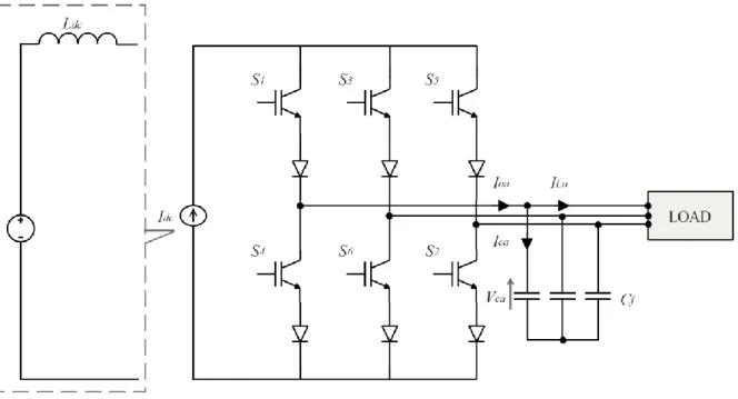
3.4 Three phase CSI ...35
3.5 CSI output current vectors ...37
3.6 Grid-connected CSI scheme ...38
3.7 CSI connected to grid through CL filter ...38
3.8 bode plot of the different CL filter configurations ...43
4.1 Block diagram of FS-MPVC control scheme ...48
4.2 FS-MPVC algorithm flowchart ...51
4.3 FS-MPVC controller scheme ...51
4.4 Proposed switching algorithm control scheme ...52
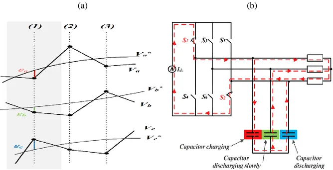
4.5 Description of switching algorithm operation principle: (a) load voltages along with their references, (b) three phase currents flow paths during first sampling interval...54
4.6 Proposed switching algorithm flowchart ...54
XII
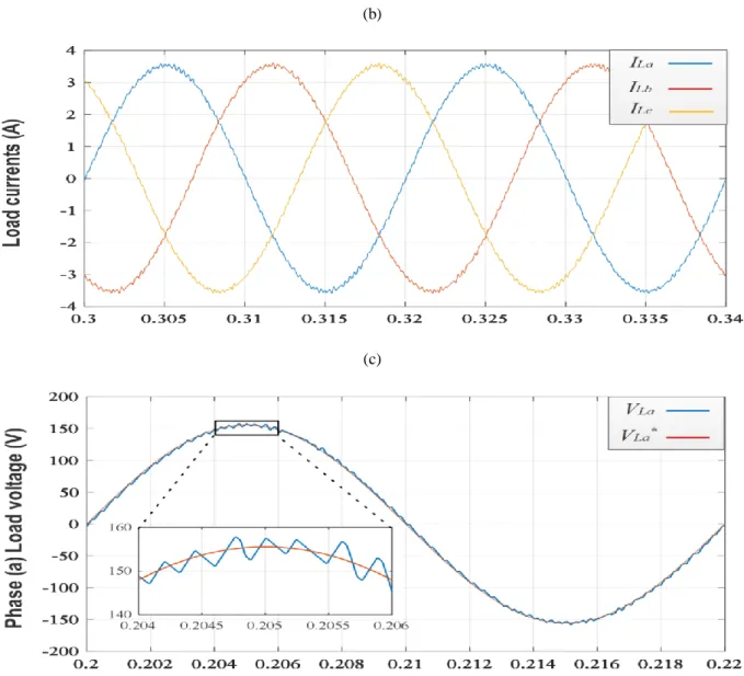
4.8 FS-MPVC responses of: (a) load voltages, (b) load currents, (c) phase (a) load voltage along
with its reference...56
4.9 Proposed switching algorithm responses of: (a) load voltages, (b) load currents, (c) phase (a) load voltage along with its reference...57
4.10 FS-MPVC responses of: (a) load voltages, (b) load currents for RL type load ...58
4.11 Proposed switching algorithm responses of: (a) load voltages, (b) load currents for RL type load... 59
4.12 Diode rectifier used as a non-linear load (Rrec=100Ω, Crec=4.7µF) ...59
4.13 FS-MPVC responses of: (a) load voltages, (b) load current for non-linear load ...60
4.14 Proposed switching algorithm responses of: (a) load voltages, (b) load currents for non-linear load ...61
4.15 FS-MPVC responses of: (a) load voltages, (b) load currents for sudden load change ...62
4.16 Proposed switching algorithm responses of: (a) load voltages, (b) load currents for sudden load change ... 63
4.17 FS-MPVC responses of: (a) load voltages, (b) load currents for sudden load change ...64
4.18 Proposed switching algorithm responses of: (a) load voltages, (b) load currents for sudden load change ...65
4.19 Obtained FS-MPVC experimental results for resistive load: (a) Load voltages (80V/div), (b) Load currents (2A/div) ...67
4.20 Obtained switching algorithm experimental results for resistive load: (a) Load voltages (80V/div), (b) Load currents (2A/div) ...67
4.21 Obtained FS-MPVC experimental results for RL type load: (a) Load voltages (80V/div), (b) Load currents (2A/div) ...68
4.22 Obtained switching algorithm experimental results for RL type load: (a) Load voltages (80V/div), (b) Load currents (2A/div) ...68
5.1 Flowchart of P&O algorithm...72
5.2 SMO sign and saturation functions ...75
5.3 Block diagram of proposed FS-MPVC control scheme ...76
5.4 DC link PI regulation loop ...77
5.5 Orientation of voltage vector on the d-axis ...77
5.6 Diagram of PI current regulation loops ...78
5.7 Active damping virtual resistor placement for FS-MPVOC ...79
5.8 Reference modification using active damping for FS-MPVOC ...80
5.9 Three-phase PLL in the synchronously rotating reference frame (SRF-PLL) ...80
5.10 Block diagram of the proposed FS-MPDPC control scheme ...81
5.11 Diagram of DC link regulation loop ...81
XIII
5.13 FS-MPDPC control algorithm flowchart ...84
5.14 Active damping resistor placement for FS-MPDPC ...85
5.15 Reference modification using proposed active damping for FS-MPDPC ...85
5.16 Performance of SMO: (a) grid current, (b) capacitor voltage, (c) grid voltage ...86
5.17 Solar irradiance level ...87
5.18 FS-MPVOC responses of: (a) PV output voltage, (b) PV output current, (c) PV output power... 88
5.19 FS-MPDPC responses of: (a) PV output voltage, (b) PV output current, (c) PV output power... 89
5.20 FS-MPVOC responses of: (a) grid d-axis current, (b) grid q-axis current ...90
5.21 FS-MPVOC responses of: (a) grid active power, (b) grid reactive power ...90
5.22 FS-MPVOC responses of phase (a) grid current and voltage ...91
5.23 FS-MPDPC responses of: (a) grid active power, (b) grid reactive power ...92
5.24 FS-MPDPC Response of phase (a) grid current and voltage ...92
5.25 FS-MPVOC responses of three phase grid currents ...92
5.26 FS-MPDPC responses of three phase grid currents ...93
5.27 System’s efficiency using FS-MPVOC ...94
5.28 System’s efficiency using FS-MPDPC ...94
5.29 FS-MPVOC responses of: (a) PV output voltage, (b) PV output current, (c) PV output power... 95
5.30 FS-MPDPC responses: (a) PV output voltage, (b) PV output current, (c) PV output power... 96
5.31 FS-MPVOC responses of: (a) d-axis grid current, (b) q-axis grid current ...97
5.32 FS-MPVOC response of: (a) grid active power, (b) grid reactive power ...97
5.33 FS-MPVOC responses of phase (a) grid current and voltage during step change in reactive power reference: (a) zoom on first step change, (b) zoom on second step change ...98
5.34 FS-MPDPC responses of: (a) grid active power, (b) grid reactive power ...99
5.35 FS-MPDPC Responses of phase (a) grid current and voltage during step change in reactive power reference: (a) zoom on first step change, (b) zoom on second step change ...99
5.36 FS-MPVOC responses of three phase grid currents ...100
5.37 FS-MPDPC responses of three phase grid currents ...100
5.38 System’s efficiency using FS-MPVOC ...101
5.39 System’s efficiency using FS-MPDPC ...101
5.40 Efficiency comparison between active and passive damping methods using: (a) FS-MPVOC, (b) FS-MPDPC ... 101
XIV
5.42 FS-MPVOC HIL responses of PV output: voltage (25V/div), current (10A/div), and power
(2kW/div) ...103
5.43 FS-MPVOC HIL responses of grid: active power (1kW/div) and reactive power (1kVAr/div)... 103
5.44 FS-MPVOC HIL responses of grid currents (10A/div) ...104
5.45 FS-MPVOC HIL responses of phase (a): grid current (20A/div) and grid voltage (80V/div) ..104
5.46 FS-MPDPC HIL responses of PV output: voltage (25V/div), current (10A/div), and power (2kW/div) ...104
5.47 FS-MPDPC HIL responses of grid: active power (1kW/div) and reactive power (1kVAr/div)... 105
5.48 FS-MPDPC HIL responses of grid currents (10A/div) ...105
5.49 FS-MPDPC HIL responses of phase (a): grid current (20A/div) and grid voltage (80V/div) ...105
5.50 FS-MPVOC HIL responses of PV output: voltage (25V/div), current (10A/div), and power (2kW/div) ...106
5.51 FS-MPVOC HIL responses of grid: active power (1kW/div) and reactive power (1kVAr/div)... 106
5.52 FS-MPVOC HIL responses of grid currents (20A/div) ...106
5.53 FS-MPVOC HIL responses of phase (a): grid current (20A/div) and grid voltage (80V/div) ..107
5.54 FS-MPDPC HIL responses of PV output: voltage (25V/div), current (10A/div), and power (2kW/div)...107
5.55 FS-MPDPC HIL responses of grid: active power (1kW/div) and reactive power (1kVAr/div)... 107
5.56 FS-MPDPC HIL responses of grid currents (20A/div) ...108
5.57 FS-MPDPC HIL responses of phase (a): grid current (20A/div) and grid voltage (80V/div) ...108
B.1 Experimental stand-alone CSI test bench ...117
B.2 CSI electrical circuit design in ISIS/ARES software ...118
B.3 Both sides of CSI prototype ... 118
B.4 CSI driver board design in ISIS/ARES software ...118
XV
List of abbreviations
AC DC DG SG RES GHG SMES ICT VSI MVSI NPC CHB ASCI LCI CSI CSR MCSI PV MPP MPPT P&O PWM SPWM CSPWM TPWM SVM SHE THD IGBT Alternating current Direct current Distributed generation Smart gridRenewable energy source Greenhouse gas
Superconducting magnetic energy storage Information and communication technology Voltage source inverter
Multi-level VSI Neutral point clamped Cascaded H-bridge
Auto-Sequentially commutated inverter Load commutated inverter
Current source inverter Current source rectifier Multi-level CSI
Photovoltaic
Maximum power point
Maximum power point tracking (tracker) Perturb & observe
Pulse width modulation Sinusoidal PWM Carrier based SPWM Trapezoidal PWM Space vector modulation Selective harmonic elimination Total harmonic distortion Insolated gate bipolar transistor
XVI RB-IGBT GCT CL TF PI PR SRF PLL FS MPC VOC DPC RL SMO HIL RT PCB Reverse blocking-IGBT Gate commutated thyristor Capacitive-inductive Transfer function Proportional integral Proportional resonant
Synchronously rotating frame Phase locked loop
Finite-Set
Model predictive control Voltage oriented control Direct power control Resistive-inductive Sliding mode observer Hardware-in-the-loop Real-time
XVII
List of symbols
The following provides definition to the symbols that are commonly used in this thesis. Other symbols which only appear in specific sections are defined in the context where they appear.
a, b, c d, q α, β Ipv Vpv Ppv Idc Io Ig Vg Ic Vc IL VL ε P Pdc Pac Q θ ω Cf Lf Rf Ldc Rdc Rd
Natural frame components
synchronously rotating reference frame components stationary reference frame components
PV array current PV array voltage PV array power DC link current CSI output current Grid current Grid voltage Capacitor current Capacitor voltage Load current Load voltage Voltage error Active power DC-side power AC-side active power Reactive power
Grid voltage vector angle Grid angular pulsation Filter capacitance Filter inductance
Internal filter inductor resistance DC link inductor inductance
Internal DC link inductor resistance Damping resistor
XVIII s Kp Ki ΔI 𝐼⃗⃗⃗⃗⃗⃗⃗ 𝑟𝑒𝑓 𝐼1 ⃗⃗ 𝑡𝑜 𝐼⃗⃗ 9 S1 to S6 S Ts g ( )op k G T Rs Rp Id Vd Iph Io Voc Isc Vt ( )n ( ),cell q Eg a k Laplace operator Proportional gain Integral gain P&O step-size
Reference current vector CSI current vectors Inverter power switches Sliding surface
Sampling time Cost function
Index of optimal value Actual sampling instant Irradiance Temperature PV Series resistance PV parallel resistance Diode current Diode voltage Photovoltaic current Saturation current Open-circuit voltage Short-circuit current Thermal voltage Index of nominal value Index of cell value
Electron charge q=1.60217646×10⁻¹⁹ C Semiconductor band gap energy
Diode ideality constant
1
Chapter 1
Introduction
1.1 Background and motivation
Electric energy consumption has been growing dramatically over the past few years to meet the energy needs related to global population and high economic growth [1.1]-[1.3]. Currently fossil fuels present the majority of electricity productions, approximately 78.4% [1.1]. The burning of fossil fuels release carbon dioxide and other greenhouse gases (GHG), as well as, many other pollutants such as sulfur dioxide and nitrogen oxides. The carbon dioxide released when fossil fuels are burned is leading to global climate change. Global GHG emissions have increased with 70% between 1970 and 2016. During this same time period, global GHG emissions from the electric energy sector have increased with about 145% [1.4].
Demand for clean, economical, and renewable energy has increased consistently over the past few decades, especially as a consequence of the energy crisis and environmental issues such as global warming and pollution. There has been a significant progress in the development of renewable energy sources such as biomass, hydropower, solar photovoltaic energy, and wind energy [1.5]-[1.16]. Approximately 19.3% of global electricity production in the world is from renewable energy sources (RES) [1.1]. The sub-divisions of RES percentages are depicted in Figure1.1
2
Among a variety of renewable energy resources available, solar energy appears to be a major contender due to its abundance and pollution-free conversion to electricity through photovoltaic (PV) process [1.5]-[1.16]. PV energy installed capacity has increased exponentially over the recent years, and has become a real alternative to boost renewable energy penetration [1.1]-[1.3], Figure 1.2 shows the worldwide cumulative PV power installed.
Figure 1.2 Evolution of cumulative PV installations (GW). [1.2]
Increasing interest in PV systems, demands growth in research and development activities in various aspects such as Maximum Power Point Tracking (MPPT), PV arrays, anti-islanding protection, stability and reliability, power quality and power electronic interface [1.15]. With increase in penetration level of PV systems in the existing power systems, these issues are expected to become more critical in time since they can have noticeable impact on the overall system performance [1.4]-[1.10]. More efficient and cost-effective PV modules are being developed and manufactured, in response to the concerns raised by the PV system developers, utilities and customers [1.4], [1.8], [1.13]. Numerous standards have been designed to address power quality and grid-integration issues [1.6]. Extensive research in the field of MPPT has resulted in fast and optimized method to track the maximum power point [1.13], [1.15].
Regarding power electronic converters to interface PV arrays to the grid, voltage source inverter (VSI) is the most used topology to date [1.16]-[1.18]. However, this topology has some limitation when it comes to PV applications. The VSI topology has buck (step-down) characteristics; therefore to step-up the low voltage output from the PV array, an extra power
2000 2001 2002 2003 2004 2005 2006 2007 2008 2009 2010 2011 2012 2013 2014 2015 2016 303 228 177 137 99 70 40 1 1 1 2 3 4 6 8 15 23 GW 50 100 250 200 150 300 350
3
electronic converter is required, this is known as dual-stage topology [1.17], [1.18]. These drawbacks can be overcome by the use another type of inverters known as Current source inverters (CSIs). CSIs appear to be direct competitors of VSIs, especially in medium, and high power applications, due to the advantages listed below [1.19]-[1.23]:
CSI outputs grid and motor friendly waveforms. Its AC voltage and current waveforms are close to sinusoidal with low harmonics distortion. It also inherently avoids high dv/dt resulting from filtering effect of output capacitors. DC-side current regulation offers an inherent current limiting, over-current, and
short-circuit protectionfeatures during AC-side faults.
The most important feature of CSI is the boosting capability, namely it can operate with a low-voltage DC source. Thus, AC voltages required in certain applications such likeuninterruptible power supply (UPS) can be obtained from a low battery voltage in one single power stage. On the other hand, PV sources can be interfaced to grid using CSI in a single-stage topology. This decreases the power losses and increases the system’s efficiency in comparison with dual-stage topologies.
Despite CSI’s many favorable features for PV application, its use has been limited due to the following drawbacks [1.19]-[1.25]:
o The on-state losses in the switching elements, where the semiconductor switches used are not capable of withstanding negative voltage, and thus have to be connected in series with a diode, this makes CSI losses higher than those in VSI. However, with new advances in the power semiconductor technologies, CSI switching losses havebeen reduced to great extent; since, insolated gate bipolar transistor (IGBT) in series with diodes could now be replaced by only one component, which is reverse-blocking IGBT (RB-IGBT).
o The losses in the DC inductor of CSI are known to be higher than those in the DC capacitor of the VSI. However, with recent developments in Superconducting Magnetic Energy Storage (SMES) technology, there is hope that concerns regarding inductor can be removed in the future.
o The AC-side filter capacitors can resonate with the filter’s inductance or distribution line inductance.
o The complexity of the control techniques represents one of the major drawbacks of CSI.
4
Though researchers have studied CSI for different applications, there still exist many points that could be investigated and improved.
Motivated by the huge demand for solar energy and immediate need for improvements in PV systems, the research reported in this thesis intends to add to the existing knowledge on PV system applications of CSI and make quality contributions to the field.
1.2 Objectives
The main objectives of the research can be summarized as follows:
To achieve a complete survey on CSIs, in terms of working principle, modeling, design, and existing modulation and control techniques.
To develop new control strategies for voltage control of CSI that could be used when switching from grid-connected to stand-alone modes due to grid disconnection of local loads during islanding of DG systems. The developed techniques should ensure fast and accurate voltage and frequency control and should also pass the robustness tests.
To develop new control strategies for single-stage three phase PV grid connected CSI. The developed strategies should be capable of extracting maximum power from the PV arrays at all insolation levels, and injecting a clean sinusoidal current into the power grid in accordance with grid codes.
To develop a sliding mode observer (SMO) observer for AC-side that must be able to estimate the required variables accurately.
To introduce active resonance damping methods for PV grid connected CSI to increase the systems efficiency and enhance the power quality.
1.3 Thesis outline
To achieve the aforementioned objectives and facilitate the presentation of results derived in the course of this research, the thesis is organized as follows:
Chapter 2 Provides a literature survey on distributed generation systems in the first part. Then, an overview of inverter topologies is presented. In the next section of the
5
chapter, the existing inverters modulation techniques and control strategies are studied and explained. Finally, literature reviews on stand-alone and grid connected CSI are performed.
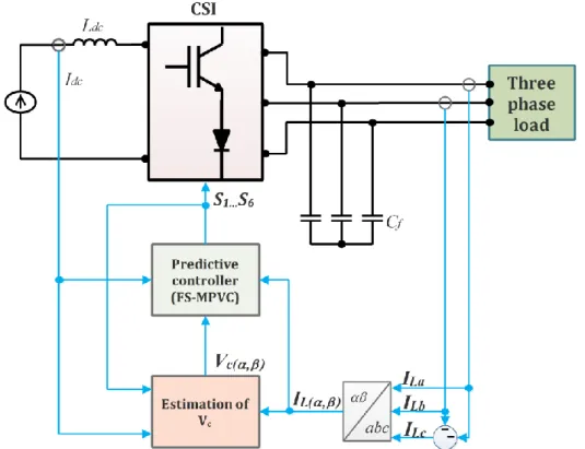
Chapter 3 Presents the design and modeling of the different components of the systems of this research. First, the PV panel has been modeled using the equivalent single diode circuit. Then, the model of CSI and its possible switching states and space vectors are exhibited. Finally, the design and modeling of the output filter have been studied. Chapter 4 Proposes new voltage control strategies for stand-alone CSIs. The developed
techniques ensure a fast and accurate voltage control independently of the type of the load, directly, i.e. without any regulations loops, and with no modulators. Simulation results using Matlab/Simulink of the proposed techniques has been carried out for different loads and during different tests. In the last part of this chapter, experimental results for a low power CSI prototype controlled by a digital signal processor (DSP) are exposed.
Chapter 5 develops a single-stage grid connected PV system based on CSI. First, it has been presented the different parts of the control strategies proposed in this chapter. Starting by the PV MPPT, where perturb and observe (P&O) algorithm is chosen due to its simplicity and good performance. A SMO is proposed for the grid-side variables estimation in order to reduce system’s cost and complexity and avoid sensor noise. After that, two novel control techniques both based on model predictive control (MPC) have been analyzed. Besides that, an active damping method for each technique is introduced instead of passive damping method. Simulation results and real-time (RT) implementation results are presented and discussed in the last part of this chapter. Chapter 6 presents the conclusions, the contributions of this research, and the
6
References
[1.1] “Renewables 2017, Global Status Report” [Online]. Available:
http://www.iea-pvps.org
[1.2] “Trends in Photovoltaic Applications 2017” [Online]. Available:
http://www.iea-pvps.org
[1.3] “Global Trends in Renewable Energy Investment 2017” [Online]. Available:
http://fs-unep-centre.org
[1.4] C. Bauer, K. Treyer, T. Heck, S. Hirschberg, “Greenhouse Gas Emissions from Energy Systems, Comparison, and Overview,” Encyclopedia of the
Anthropocene, Vol. 1, No. 1, Jan. 2018, pp. 473–484
[1.5] F. Blaabjerg, D. M. Ionel, “Renewable Energy Devices and Systems – State-of-the-Art Technology, Research and Development, Challenges and Future Trends,” Electric Power Components and Systems, Vol. 43, No. 12, Jul. 2015, pp. 1319–1328
[1.6] M. G. Simoes, F. A. Farret, Modeling Power Electronics and Interfacing Energy
Conversion Systems, John Wiley & Sons, Ltd, 2017.
[1.7] Y. Wu, J. Lin, H. Lin, “Standards and Guidelines for Grid-connected Photovoltaic Generation Systems: a Review and Comparison,” IEEE Trans. on
Industry Applications, Vol. 53, No. 4, Mar. 2017, pp. 3205–3216
[1.8] A. Anzalchi, A. Sarwat, “Overview of Technical Specifications for Grid-Connected Photovoltaic Systems,” Energy Conversion and Management, Vol. 152, No. 15, Nov. 2017, pp. 312–327
[1.9] O. P. Mahela, A. G. Shaik, “Comprehensive Overview of Grid Interfaced Solar Photovoltaic Systems,” Renewable and Sustainable Energy Reviews, Vol. 68, No. 1, Feb. 2017, pp. 316–332
[1.10] F. L. Lyo, H. Ye, Advanced DC/AC Inverters Application in Renewable Energy. CRC Press, 2013.
[1.11] D. Rekioua, E. Matagne, Optimisation of Photovoltaic Power Systems:
Modelisation, Simulation, and Control. Springer-Verlag, 2012.
[1.12] H. Abu-Rub. M. Malinowski, K. Al-Haddad, Power Electronics for Renewable
Energy Systems, Transportation, and Industrial Applications. John Wiley &
7
[1.13] Z. Mirhassani, H. C. Ong, W. T. Chong, K. Y. Lyong , “Advances and Challenges in Grid Tied Photovoltaic Systems,” Renewable and Sustainable
Energy Reviews, Vol. 49, No. 1, Sep. 2015, pp. 121–131
[1.14] Q. Zhong, T. Hornik, Control of Power Inverters in Renewable Energy and
Smart Grid Integration. John Wiley & Sons, Ltd, 2013.
[1.15] N. Femia, G. Petrone, G. Spagnuolo, M. Vitelli, Power Electronics and Control
Techniques for Maximum Energy Harvesting in Photovoltaic Systems. CRC
Press, 2013.
[1.16] R. Teodorescu. M. Liserre, P. Rodriguez, Grid Converters for Photovoltaic and
Wind Power Systems. John Wiley & Sons, Ltd, 2011.
[1.17] M. Islam, S. Mekhilef, M. Hasan “Single Phase Transformerless Inverter Topologies for Grid-tied Photovoltaic System: A Review,” Renewable and
Sustainable Energy Reviews, Vol. 45, No. 1, May. 2015, pp. 69–86
[1.18] C. Photong, C. Klumpner, P. Wheeler, “Evaluation of Single-Stage Power Converter Topologies for Grid-Connected Photovoltaics,” in Proc. IEEE Int.
Conf. on Industrial Technology, Chile, 2010, pp. 1161–1168.
[1.19] B. Sahan, S. V. Araujo, C. Noding, P. Zacharias, “Comparative Evaluation of Three-Phase Current Source Inverters for Grid Interfacing of Distributed and Renewable Energy Systems,” IEEE Trans. on Power Electronics, Vol. 26, No. 8, Aug. 2011, pp. 2304–2318
[1.20] B. K. Bose, Modern Power Electronics and AC drives, Prentice Hall PTR, 2002. [1.21] B. Wu, High-power Converters and AC drives, John Wiley & Sons, Ltd, 2006. [1.22] M. H. Rashid, Power Electronics Handbook, Third Edition,
Butterworth-Heinemann, Ltd, 2011.
[1.23] P. P. Dash, M. Kazerani, “Dynamic Modeling and Performance Analysis of a Grid-Connected Current-Source Inverter-Based Photovoltaic System,” IEEE
Trans. on Sustainable Energy, Vol. 2, No. 4, Oct. 2011, pp. 443–450
[1.24] Y. W. Li, “Control and Resonance Damping of Voltage-Source and Current-Source Converters With LC Filters,” IEEE Trans. on Industrial Electronics, Vol. 56, No. 5, Nov. 2008, pp. 1511–1521
[1.25] S. Jayalath, M. Hanif, “CL-Filter Design for Grid Connected CSI,” in Proc.
8
Chapter 2
Literature survey
2.1 Introduction
The rapid depletion of fossil based energy resources such as coal, natural gas and oil, together with an effort to reduce CO2 emission into the atmosphere has required a demand for a larger share of clean energy to be produced from renewable energy sources (RES). Recently, there has been a great interest on distributed generation (DG) in order to replace the conventional electrical distribution systems and achieve better performance and management of energy. In this chapter; a brief review on DG trends has been presented. DG systems can be sourced by different renewable energy sources such as photovoltaic (PV), wind, and others. The focus in this chapter was on photovoltaic energy, where the electricity generation process is discussed and the possible grid integration configurations are presented. Generally, there exist two configuration single- and dual-stage. In dual-stage configuration the generator side converter is responsible for the extraction of the maximum power, whereas the grid-side converter is responsible for injecting the resulting power in a suitable form. Nevertheless, in single-stage configuration the inverter can fulfill both control objectives. A classification and description of the most common inverter topologies used to interface PV systems is done in the third part of this chapter. In the next section, different modulation techniques of current source inverter (CSI) have been exposed and analyzed. Finally literature reviews on stand-alone and grid-connected CSIs are completed to evaluate the state of the art of available control strategies.
2.2 Distributed generation systems
The existing power grids can be considered as a hierarchical systems where power plants are at the top of the chain and loads are at the bottom, resulting in a unidirectional electrical power flow managed with limited informations about the exchange between sources and terminal points. This situation present serious drawbacks, including the following [2.1]-[2.2]:
o System sensitivity to voltage and frequency instabilities as well as to power security problems caused by load variations and dynamic network reconfigurations.
9
o Risks of failures and blackouts and decreased system efficiency. o Unsuitability for the integration of renewable energy.
During the last decade, the electrical energy market has been characterized by a growing demand for energy and two important innovations: the quick growth and massive diffusion of RESs and the subsequent rapid development of DG systems and smart grids (SGs) [2.1]–[2.5]. The basic gist of DG is the process of generating energy close to its point of delivery. So, rather than having a big power plant (coal, nuclear, hydroelectric, etc.) that generates massive amounts of energy, which is then transmitted over a vast and complicated network of power lines and transfer stations to be delivered to eventual homeowners or businesses, smaller power plants that generate a moderate amount of energy are located at closer proximity to the homes and businesses that will use it. [2.2]
According to many analyses, future electrical systems should have the following parameters [2.2],[2.3]:
High power capability: electricity is becoming the main power source of the modern world and hence the need for it will increase significantly during the next years, this trend is expected to remain positive for many decades and will be marginally influenced by external perturbations such as economic or political crises.
High power quality and reliability: electricity must be available whenever it is needed with the lowest or no latency, stable voltage and frequency and low harmonic distortion. High efficiency: electricity should not be dispersed during production, transportation and distribution processes. The grid and the loads should be managed to achieve maximum system efficiency.
High flexibility: the power system should be highly configurable and should allow smooth integration among different power sources, moreover, dynamic changes of loads and power sources should not influence system performance and power quality.
Low environmental impact: renewable energy sources should progressively replace traditional polluting sources.
Previous requirements cannot be satisfied by conventional power systems, therefore, during the next years a huge revision of the present systems is expected with the introduction of many new functionalities, systems, commonly referred to as DG and SG revolution. This is changing the way in which next generation power systems have to be designed, operated and maintained,
10
and can be achieved only by introducing new technologies, functionalities and operational approaches, which are as follows [2.1]–[2.3]:
Full exploitation of all renewables.
Technological enhancements and large-scale diffusion of energy storage systems. Massive introduction of Information and Communication Technologies (ICTs).
Implementation of high-granularity self-healing and resiliency against unwanted situations, such as blackouts or natural disasters.
Consumers’ active participation to the electricity market. Introduction of new products, services and markets.
2.2.1 Distributed generators
As it has been mentioned above, it is necessary for the engineering society to pay more interest on the researches of RESs. There exist many forms of renewable energy resources that are currently available for the integration into the power grid, the top four energy sources are wind, solar photovoltaic, hydroelectric, and geothermal. Only photovoltaic generator will be discussed in this section, since it presents the subject of this research.
2.2.1.1 Photovoltaic generators
PV cells are direct current (DC) generatorswhich use semiconductor technology to transform the energy in sunlight into electricity. Silicon is the most widely used semiconductor material in PV cell, which consists of a junction consisting of n- and p-doped silicon. When light (photons) strikes the junction, the energy in the photons is converted to electric power. The voltage level of PV cells depends on the intrinsic cell characteristics, the number of cascaded cells and their temperature, whereas the available current depends on cell characteristics, the number of parallel strings (a string is a group of cascaded cells) and sunlight irradiation. With present technology, they are arranged in panels providing up to 220–250 W at a voltage rating of 48–60 V [2.6],[2.7].
In order to supply standard loads operating with alternating current (AC), panels are connected in series and/or in parallel, thus reaching the desired level of voltage and current, to supply an inverter [2.7]. PV sources can also feed the distribution grid using a suitable conversion chain. Generally a PV system connected to the grid can be either in single- or dual-stage configurations. Figure 2.1. However, single-stage configuration can fulfill all the control objectives with lower switching losses, and thus, providing higher efficiency. [2.2],[2.6],[2.7]
11
Figure 2.1 Schematic diagram of photovoltaic grid-connected system configurations:
(a) Single-stage (b) Dual-stage.
2.3 Inverter topologies
The power electronic interface is an important part of DG units as it influences the overall system efficiency and performance [2.7]. Many converter types have been used for this purpose, depending on the DG source, system requirements, and control objectives. In PV applications, DC-DC converters and DC-AC inverters are needed to ensure MPPT and efficient power conversion into AC loads. However, in single-stage configuration only DC-AC inverters are required to interface PV sources to the distribution grid.
Fundamentally, as shown in Figure 2.2, there are two types of inverters existed, the voltage source inverter (VSI) and the current source inverter (CSI). In general, an inverter that exploits the input voltage while producing controlled output voltage is classified as VSI whereas an inverter that exploits the input current while producing controlled output current is classified as CSI. The VSI is the more mature and proven technology where it has been successfully implemented in industry for decades [2.6]-[2.10]. While the 2-Level VSI has found applications in many conventional industrial machines, the multi-level VSIs (MVSIs) are more recent and established in industry due to their advantages in particular the ability to generate multilevel stepped-waveform with reduced harmonic distortion, and to reach higher voltage operation, and higher modularity [2.6]. On the other hand, the auto-sequentially commutated inverter (ASCI) and the load-commutated inverters (LCI) and are among the earliest inverters used for variable speed drives before slowly being replaced by the pulse-width modulation (PWM) CSI mostly
12
in induction motor drives. Quite recently, similar to the VSIs, multi-level CSIs (MCSIs) are gaining attention in new research activities [2.8],[2.10]. While both types of inverters have substantial differences topologically, they do share the same working principles. Thus, in general, common control methods and common power semiconductor switches used for VSI can also be applied to CSI with some modifications.
Figure 2.2 Inverters classification
Today the majority of the worldwide installed power inverters are VSIs followed by CSIs. CSIs are available in industrial drives, and have also been connected to wind power and solar power generators and fuel cell systems. Comparison between VSIs and CSIs have been reported many times [2.11] concluding that the decision lies with the performance of the application. Both inverters, however, face the same challenges. Generally they have to be small, light and cost-effective and technically they have to operate at high efficiencies, produce low harmonics, and be simple to control and reliable. For high voltage and high current application this has led to the introduction of multi-level topologies, first for VSIs like the diode-clamped, flying capacitor and cascaded topologies and later to CSIs [2.6]-[2.10]. With the dominating VSI market research into MCSI has been limited. The reason for the lag of interest is, beside the dominance of the VSI in the market, the large component count that is required to build MCSI in particular for a level higher than five i.e. an existing nine-level CSI requires three inductors and twelve power switches. This number goes up rapidly when upgrading the inverter to even higher level of currents. For example a seventeen-level CSI can have seven inductors and twenty power switches.
13
2.3.1 Voltage source inverters
The primary function of a VSI is to convert a fixed DC voltage to a three-phase AC voltage with variable magnitude and frequency. This section discusses the different VSI topologies used commonly in DG systems, and highlights description and features of each one. The topologies discussed are two-level and multi-level VSI. MVSI can be subdivided into three main topologies: cascaded H-bridge (CHB), diode-clamped, flying capacitor.
2.3.1.1 Two-level VSI
A simplified circuit diagram for a two-level VSI for high-power medium-voltage applications is shown in Figure 2.3. The inverter is composed of six groups of active switches with a free-wheeling diode in parallel with each switch. Depending on the DC operating voltage of the inverter, each switch group consists of two or more IGBT or gate commutated thyristor (GCT) switching devices connected in series [2.6]-[2.10].
Figure 2.3 Three phase VSI 2.3.1.2 Multi-level VSIs
A. Cascaded H-bridge
CHB multilevel inverter is one of the popular converter topologies used in high-power medium-voltage (MV) drives. It is composed of a multiple units of single-phase H-bridge power cells. The H-bridge cells are normally connected in cascade on their AC side to achieve medium-voltage operation and low harmonic distortion [2.7].
14 B. Neutral point clamped inverters
The diode-clamped multilevel inverter employs clamping diodes and cascaded DC capacitors to produce AC voltage waveforms with multiple levels. The inverter can be generally configured as a three or more levels topology, but only the three-level inverter, often known as neutral-point clamped (NPC) inverter, has found wide application in high-power medium-voltage drives. The main features of the NPC inverter include reduced dv/dt and THD in its AC output voltages in comparison with the two-level inverter discussed earlier. More importantly, the inverter can be used in the medium voltage drive to reach a certain voltage level without switching devices in series. [2.7]-[2.10]
C. Multi-level flying capacitor
It is evolved from the two-level inverter by adding DC capacitors to the cascaded switches. There are four complementary switch pairs in each of the inverter legs. Therefore, only four independent gate signals are required for each inverter phase. The flying-capacitor inverter can produce an inverter phase voltage with five voltage levels. [2.7]
2.3.2 Current source inverters
The CSI (also called current fed inverter) converts the input DC current into three phase AC currents. In CSI, the input current remains constant but could be adjustable. The output currents of a CSI are independent of the load. Nevertheless, the load voltage are dependent of load. This section discusses the different three phase CSI topologies which are subdivided according to their type of commutation into forced-commutated, and natural commutated CSIs (PWM CSIs). The forced-commutated CSIs which are ASCI and LCI represent the earliest types of CSIs. However, the development of power electronics and fast switching devices have permitted lately the appearance of two-level and multi-level (parallel) PWM CSIs.
2.3.2.1 Auto-sequentially commutated inverter
The conventional auto-sequentially commutated inverter (ASCI) shown in Figure 2.5 has six thyristors connected in series with a diode for each. A respective commutating capacitor is interconnected between the junctures of the thyristor and diode of each respective branch sub-circuit and the thyristor and diode of the next adjacent branch sub-sub-circuit. ASCI inverters were developed especially for high power variable-speed drives. The major drawbacks of this topology is limited control strategies applicable since a thyristor cannot be switched off. [2.10]
15
Figure 2.4 Auto-Sequentially commutated inverter 2.3.2.2 Load commutated CSI
The thyristor-based LCI is also one of the earliest inverters developed for variable-speed drives. A three-phase LCI has three parallel legs represented by two series connected thyristors per leg, which in total requires six thyristors. An AC capacitor filter is installed at the output of LCI in order to reduce harmonics content. As shown in Figure 2.6, the thyristor switches are numbered according to their firing sequence. The same major drawback reported for ASCIs is present for LCI, since a thyristor can only be switched on intentionally, Therefore, the most common control technique applied is the six-step switching, in which each thyristor conducts for 120° degrees interval. [2.10]
Figure 2.5 Load commutated CSI 2.3.2.3 Two-level CSI
An idealized PWM CSI is shown in Figure 2.4. The inverter is composed of six unidirectional devices, each of which can be replaced with two or more devices in series for medium-voltage
16
operation. The switching devices used in the CSI are of symmetrical type with a reverse voltage blocking capability. The inverter produces a defined PWM output current. The DC side of the inverter is an ideal DC current source Idc. In practice, Idc can be obtained by a current source
rectifier (CSR) or a current controlled buck converter [2.8]-[2.10].
Figure 2.6 Ideal three phase CSI 2.3.2.4 Multi-level CSIs
To increase the power of a CSI, two or more CSIs can be connected in parallel to form a MCSI. Figure 2.7 shows such a configuration where two inverters are connected in parallel. Each inverter has its own DC current source, while they share the same capacitor filter at their outputs. The main issue of this topology is the number of inductors and the unbalance of DC currents. [2.8]
17
2.4 Inverters control
The purpose of the inverter in a DG system is to convert the raw power generated into a form compatible with the local distribution grid, in order to allow the power to be used by standard appliances or to be fed back into the utility grid. Therefore, suitable inverter modulation techniques and control strategies are of high importance to satisfy all the control objectives of the DG system [2.6].
As reported previously, VSI represents the most widely used topology in industrial applications. Consequently, its modulation techniques are well-known, and have been reported widely in the literature. VSI modulation techniques include sinusoidal pulse width modulation (SPWM), third harmonic injected PWM (THIPWM), space vector modulation (SVM) and Selective harmonic elimination (SHE). In the other hand, several control strategies and methods have been investigated and developed by researchers for VSI, Figure 2.8 show the most common VSI control strategies. [2.6]-[2.10]
18
In contrast, CSI modulation techniques are less-known compared to those of VSI. Moreover CSI control strategies are less developed and less investigated in the literature. Therefore, the following sections focus only on giving a detailed analysis of CSI modulation techniques and providing literature reviews of CSI control strategies for both stand-alone and grid-connected modes.
2.4.1 CSI modulation techniques
Various modulation techniques have been developed for the PWM CSI, including carrier-based sinusoidal PWM (CSPWM), Trapezoidal PWM space vector modulation (SVM), and selective harmonic elimination (SHE). Generally the switching pattern design for the CSI should generally satisfy two constraints: (1) The DC current should have a path at any time, (2) The output current of CSI should be defined. Thus, at any instant one and only one upper switch, and one and only one lower switch should be conducting. [2.8]-[2.10]
2.4.1.1 Carrier-based SPWM
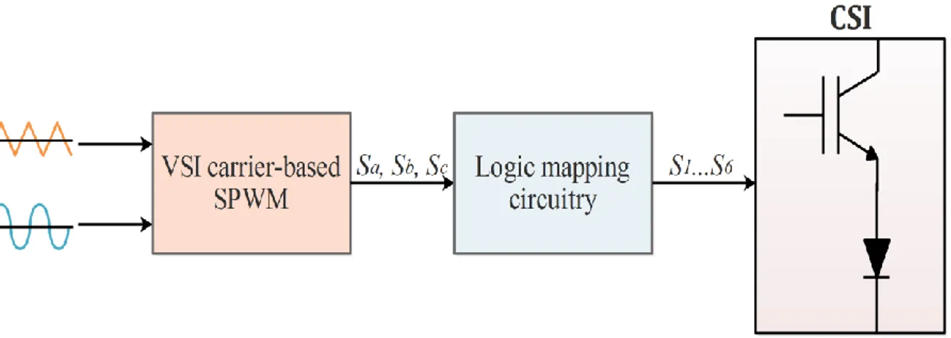
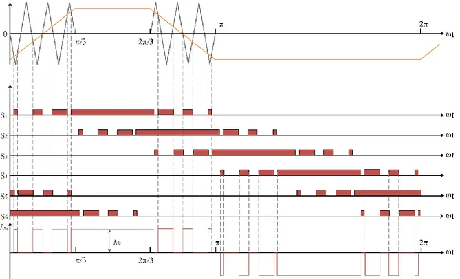
A. SPWM VSI to CSI state map [2.12]
Carrier-based SPWM is simple to implement in a VSI and can be realized with a relatively low switching frequency. However, implementation of CSI carrier-based SPWM is not as straightforward as for the VSI case. The common approach used for the implementation of CSI carrier-based SPWM is to modify the gating signals of the VSI PWM using logic mapping circuitry.
Figure 2.9 depicts the principle of CSI switching signals generation using SPWM VSI to CSI state map modulation technique.
19 B. Bi-logic/tri-logic PWM [2.13]
Bi-logic/tri-logic PWM is carried out using simple SPWM that generates Xa, Xb, Xc two-level
signals (+1,-1) which are then transformed to tri-logic (-1,0,+1) PWM variables Ya, Yb, Yc via a
transformation matrix as follows
c b a c b a X X X Y Y Y 1 0 1 1 1 0 0 1 1 2 1 (1)
The resulting tri-logic PWM variables satisfy always the following equation
0
b c aY
Y
Y
(2)Finally, the tri-logic signals are used by gating logic block to trigger the power switches of CSI, in such a way that the pth CSI output current I
op is given in terms of Yp and DC current Idc as
dc p op
Y
I
I
(3)However, it has to be pointed out that the tri-logic state (Ya=Yb=Yc=0) can be realized by
short-circuiting one of the CSI legs (freewheeling state)
According to the above analysis, it can noted that this modulation technique fulfills always the CSI switching constraints.
Table2.1 lists all possible bi-logic and tri-logic states with their corresponding switching signals Table 2.1 CSI bi-logic/tri-logic states with corresponding switches triggering signals
Bi-logic signals Tri-logic signals Upper switches Lower switches
Xa Xb Xc Ya Yb Yc S1 S3 S5 S2 S4 S6
+1 +1 +1 0 0 0 Freewheeling through one of CSI legs
+1 +1 -1 0 +1 -1 0 1 0 1 0 0 +1 -1 +1 +1 -1 0 1 0 0 0 0 1 +1 -1 -1 +1 0 -1 1 0 0 1 0 0 -1 +1 +1 -1 0 +1 0 0 1 0 1 0 -1 +1 -1 -1 +1 0 0 1 0 0 1 0 -1 -1 +1 0 -1 +1 0 0 1 0 0 1
20
Figure 2.10 shows the block diagram of bi-logic/tri-logic modulation technique.
Figure 2.10 Diagram of bi-logic/tri-logic modulation technique 2.4.1.2 Trapezoidal PWM
The principle of TPWM is similar to PWM applied in VSIs, where the gate signals for one switch are generated by comparing the trapezoidal modulator with a defined triangular carrier. [2.8]. The gate signals of the rest of switches are derived by phase shifting by the gate signals of the previous switch as shown in Figure 2.8.
21 2.4.1.3 Space vector modulation (SVM)
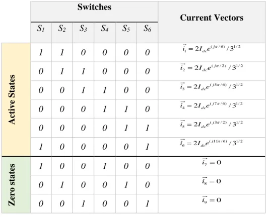
Similar to VSIs, CSIs can also be controlled using SVM technique. To satisfy the aforementioned CSI switching constraints, the CSI can output nine current vectors in the stationary reference frame αβ, of which six are active vectors and three are null vectors. Table 2.1.
Table 2.2 CSI switching states and space vectors
Switches Current Vectors S1 S2 S3 S4 S5 S6 A cti ve S tate s 1 1 0 0 0 0 2 / 1 ) 6 / ( 1 2 /3 j dce I i 0 1 1 0 0 0 2 / 1 ) 2 / ( 2 2 /3 j dce I i 0 0 1 1 0 0 2 / 1 ) 6 / 5 ( 3 2 /3 j dce I i 0 0 0 1 1 0 2 / 1 ) 6 / 7 ( 4 2 /3 j dce I i 0 0 0 0 1 1 2 / 1 ) 2 / 3 ( 5 2 /3 j dce I i 1 0 0 0 0 1 2 / 1 ) 6 / 11 ( 6 2 /3 j dce I i Ze ro s tate s 1 0 0 1 0 0 i7 0 0 1 0 0 1 0 i8 0 0 0 1 0 0 1 i9 0
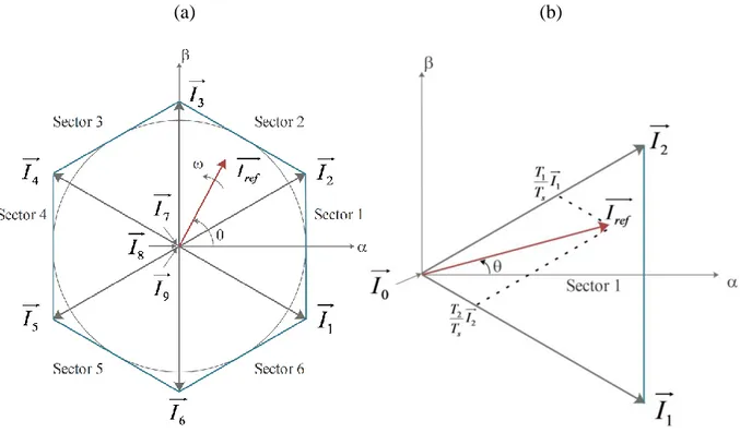
A typical space vector diagram for the CSI is shown in Figure 2.9 (a), where 𝐼⃗⃗ to 𝐼1 ⃗⃗⃗ are active 6 vectors, and 𝐼⃗⃗⃗ to 𝐼7 ⃗⃗ are zero vectors symbolized for simplification as 𝐼9 ⃗⃗⃗ . The active vectors 0 form a regular hexagon with six equal sectors, whereas the zero vector lies in the center of the hexagon.
For a given length and position, 𝐼⃗⃗⃗⃗⃗⃗⃗ can be synthesized by two adjacent vectors and one zero 𝑟𝑒𝑓
vector based on the ampere-second balance principle, that is, the product of the reference vector 𝐼𝑟𝑒𝑓
⃗⃗⃗⃗⃗⃗⃗ and the sampling period Ts equals the sum of the current vectors by the timeinterval of
chosen space vectors [2.8]-[2.10]. Figure 2.9 (b). The ratio between the magnitudes of output current and the DC link current determines the modulation index ma, and is defined as the
22
(a) (b)
Figure 2.9 CSI SVM scheme: (a) space vector diagram (b) Synthesis of reference vector in sector 1
The ampere-second balancing equation is thus given by
0 2 1 0 0 2 2 1 1 T T T T T I T I T I T I s s ref (4)
The vector dwelling times can be derived by solving equations in (4)
2 1 0 0 2 1 ) sin( ) 3 / sin( T T T T T m T T m T s a s a
(5)Once the vector dwelling times are calculated, the vector sequence in a sampling period needs to be determined for the generation of PWM pulses. Different sequence patterns can be generated in function of zero vector used for each sampling time and its placement to achieve the desired switching frequency and harmonic profile.
2.4.1.4 Selective harmonic elimination
The SHE technique is an offline modulation scheme that can eliminate a number of unwanted low-order harmonics with a limited number of pulses. In this technique, the switching angles are pre-calculated and then imported into a digital controller for implementation [2.10]. In order to achieve a better harmonic profile and to reduce the complexity in finding switching pattern
23
solutions, the calculated pulses are normally arranged in such a way that the derived PWM waveform has a quarter-wave symmetrical shape. In high power applications, where the SHE is usually preferable, low switching frequency is needed to reduce the losses. Therefore, three, five or seven switching angles per quarter of cycle are preferred [2.9]. In the case shown in Figure 2.10, five pulses are employed. This figure shows a typical SHE pattern that satisfies the CSI switching constraint. There are five pulses per half cycle with five switching angles in the first /2 period. However, only two out of the five angles, i.e., 1 and 2 are independent. Given
these two angles, all other switching angles can be derived [2.8].
The two switching angles provide the ability to eliminate two harmonics such as the 5th and 7th harmonic from the inverter output current. This can be considered as the main advantage of this technique, since this is hardly possible by using other modulation techniques to remove these low order harmonics. Nevertheless, the main disadvantage of this technique is the lack of flexibility for control as the offline calculated set of angles is valid at only a certain modulation index. Moreover, the calculation of SHE angles with a large number of pulses per fundamental cycle sometimes involves transcendental equations that have no solutions, which prevents the SHE from being applied to a full frequency range.[2.10]
Figure 2.10 Selective harmonic elimination (SHE) PWM pattern
Table 2.2 Comparison of most common CSI modulation techniques [2.8]
Item TPWM SVM SHE
Modulation index 0.74 0.707 0.73-0.78
Dynamic performance Medium High Low
Digital implementation Real time/
Look-up table Real time Look-up table
Harmonic performance Good Adequate Best
DC current
24
The table above presents a comparison between the three most common modulation techniques which are TPWM, SVM, and SHE. It is obvious that SVM is the more adequate technique due the features it offers, especially the fast dynamic. However SHE is the best choice in terms of harmonics elimination. But, it has to be pointed out that TPWM is simplest technique for digital implementation.
2.5 Literature review of CSI based stand-alone systems
There exist numerous researches on stand-alone CSIs feeding linear and non-linear loads. Some of them address voltage regulation, whereas the rest consider current control only. Among the proposed current control strategies reported in the literature: In [2.14] SVM is utilized and analyzed in details, whilst in [2.15] a modified SVM named direct regular sampled SVM is proposed. It is based on the modification of the switching sequences of conventional SVM, in order to reduce the switching frequency. Authors in [2.16] proposed a predictive current control strategy and addressed the issue of reducing switching frequency also. A 7 switches (CSI7) topology with a new modulation technique have been proposed in [2.17]. The purpose was to achieve lower switching frequency and reduce the size of the inductor and attain high performances. In [2.18] it has been proposed a four leg CSI to overcome the problem of common-mode voltage.
Though these control technique offer a suitable current control, voltage control is required for standalone systems, since the majority of loads need a defined voltage for their operation. The available researches on voltage control for stand-alone CSIs [2.19]-[2.24] are achieved through current control by employing controllers and voltage regulation loops that are designed and tuned for a predefined load types and values. Hence, their stability and accuracy are not guaranteed for change in load. This problem has been overcome in this thesis.
2.6 Literature review of CSI based grid connected systems
A fair amount of researches have been carried out for grid connected CSI systems. The available researches focused in general on the following points:
Modified CSI topologies: In [2.25] a PV grid connected CSI is introduced using a double-tuned parallel resonant circuit to attenuate the second- and fourth-order harmonics at the inverter DC side, and proportional-resonant (PR) current controller along with a modified carrier based modulation technique. In [2.26], a multi-level structure based on CSI topology is presented. Each inverter unit in the multi-level
![Figure 1.1 Estimated renewable energy share of total final energy consumption, 2016 [1.1]](https://thumb-eu.123doks.com/thumbv2/123doknet/3466238.101266/20.892.151.742.843.1092/figure-estimated-renewable-energy-share-total-energy-consumption.webp)