T
T
H
H
È
È
S
S
E
E
En vue de l'obtention du
D
D
O
O
C
C
T
T
O
O
R
R
A
A
T
T
D
D
E
E
L
L
’
’
U
U
N
N
I
I
V
V
E
E
R
R
S
S
I
I
T
T
É
É
D
D
E
E
T
T
O
O
U
U
L
L
O
O
U
U
S
S
E
E
Délivré par l'Université Toulouse III - Paul SabatierDiscipline ou spécialité : Génie Eléctrique
JURY
Prof.Eric MONMASSON (rapporteur) Prof. Miro MILANOVIC (rapporteur)
Dr. Javier CALVENTE (rapporteur) Prof. Sigmond SINGER (examinateur) Prof. Alexandre NKETSA (examinateur)
Ecole doctorale : GEET Unité de recherche : LAAS-CNRS
Directeur(s) de Thèse : Prof. Corinne ALONSO (directrice), Dr. Vincent BOITIER (co-directeur) et M. Jean-Louis Chaptal (co-directeur)
Présentée et soutenue par Adán SIMON MUELA Le 24 de Novembre de 2008
Titre :
Architectures de Convertisseurs DC/DC basse tension et fort courant avec commande numérique
AUTEUR: Adán SIMON‐MUELA TITRE: Architectures de Convertisseurs DC/DC à fort courant, basse tension avec commande numérique DIRECTEUR DE THESE: Prof. Corinne Alonso et Dr. Vincent Boitier LIEU ET DATE DE SOUTENANCE: Toulouse, 24 de novembre de 2008 RESUME:
La consommation de puissance des microprocesseurs embarqués ne cesse d’augmenter avec la multiplication des fonctions qu’ils doivent assurer Ainsi, les générations actuelles de microprocesseurs ont une forte consommation en courant sous une très faible tension (autour du volt) avec des transitoires contraignants.
Cette thèse est consacrée à la design des systèmes d’alimentation rapprochées des cartes mères des PC où régulateurs de tension (VRMs) qui englobent fort courant et faible tension de sortie ainsi que haute fréquence de découpage. A cet effet, les architectures entrelacées ou multi-phase sont une bonne alternative pour atteindre ces niveaux énergétiques si rigoureux.
Traditionnellement, ces types de systèmes d’alimentation sont contrôlés avec une commande analogique. Cependant, les nouvelles générations de microprocesseurs exigent des performances plus élevées en même temps qu’une régulation plus précise. Alors, la commande classique analogique est de plus en plus remplacée par une commande numérique plus flexible et plus performante.
Cette thèse s'intègre dans le cadre du projet régional LISPA où le LAAS et Freescale Semiconductor collaborent pour développer de nouveaux systèmes d’alimentations pour microprocesseurs de puissance.
MOTS‐CLES: PoL, VR, multiphase, mode entrelacé, commande numérique, FPGA, DSC DISCIPLINE ADMINISTRATIVE: Génie Electrique ADRESSE DU LABORATOIRE: 7, Av. Colonel Roche, 31077, Toulouse, France
AUTHOR: Adán SIMÓN‐MUELA
TITLE: Architectures of High‐Current, Low‐Voltage, Digitally‐Controlled DC/DC Power Converters DIRECTORS: Prof. Corinne Alonso and Dr. Vincent Boitier PLACE AND DEFENSE DATE: Toulouse, November, 24th, 2008 ABSTRACT:
The power consumption of embedded microprocessors has increased significantly due to the considerable number of new functions which they should manage. Thus, current generation of microprocessors needs considerable supply currents with very low voltages.
The aim of this dissertation is to study these supply modules and their association to increase the current supply levels delivered to the charge. These power supply systems are oriented to embedded microprocessors like those can be found inside PC motherboards..
Traditionally, this kind of power supplies owns analogue control. However, new
microprocessor generation demands faster performances and more accurate and tight regulations. Thus, the present trend is to replace the classical analogue control by a digital control system more flexible and performing likewise.
Then, this dissertation takes part in the LISPA regional project where the LAAS and Freescale Semiconductor collaborate to develop new power supply systems for embedded power microprocessors.
KEYWORDS: PoL, VR, multiphase, interleaving mode, digital control, FPGA, DSC DISCIPLINE ADMINISTRATIVE: Electric Engineering
R
EMERCIEMENTS-
A
CKNOWLEDGEMENT–
A
GRADECIMIENTOSCette thèse CIFRE est le résultat de travaux de recherche développés pendant ces trois années de thèse au sein du groupe ISGE du LAAS-CNRS dirigé par Mme. Marise Bafleur et au sein du groupe TSO de Freescale mené par M. Jean-Louis Chaptal dans le cadre du laboratoire commun LISPA. Je tiens à les remercier de m’avoir accueilli dans leur service respectif et dans les meilleures conditions possibles et de m’avoir fait confiance malgré certains changements d’équipe et de direction.
Je tiens également à remercier Madame le professeur Corinne Alonso, et le Docteur M. Vincent Boitier, mes responsables scientifiques au sein du LAAS, pour leur patience et les précieux conseils qu’ils m’ont donné tout au long de ces trois années.
J’aimerais aussi remercier les rapporteurs le Professeur Eric Monmasson, le Professeur Miro Milanovic et le Docteur Javier Calvente pour leurs avis et appréciations sur ce travail. Je n’oubli pas les membres du jury le Professeur Alexandre Nketsa et le Professeur Sigmond Singer qui ont accepté de juger ces travaux de thèse.
Le travail ici présenté est le fruit d’un travail en équipe dans lequel plusieurs personnes ont diligemment collaboré. Je tiens d’abord à remercier M. Lionel Séguier and M. Cyril Lahore pour leur savoir-faire dans les réalisations pratiques de cette thèse.
Aussi, je voudrais remercier les étudiants qui m’ont aidé pendant ces années : M. Youssef Elbasri, M. Joseph Fabre, M. Lionel Duluc, M. Bruno Vincent et M. Javier Martinez Garcia-Tenorio.
Finalement, je n’oublie pas mes collègues de thèse et autres personnes avec lesquelles j’ai passé de remarquables moments au LAAS et qui m’ont facilité mon intégration dans ce beaux pays : Bruno, Pierre, Philippe, Cédric, Stéphane, Jeff, Aloña, Alain…
This CIFRE dissertation is the final result of the 3-year research work made in the ISGE group of the LAAS-CNRS directed by Ms. Marise Bafleur and the TSO team of Freescale Semiconductor leaded by Mr. Jean-Louis Chaptal thanks to their collaboration in the LISPA common laboratory. Therefore, I thank them to accept me in their respective research teams.
I also want to thank my scientific directors in the LAAS-CNRS Prof. Corinne Alonso and Dr. Vincent Boitier who they give me precious advises along this three years of hard work.
I also express my gratitude to my reviewers Prof. Eric Monmasson, Prof. Miro Milanovic and Dr. Javier Calvente for their notable recommendations as well as the members of the jury Prof. Alexandre Nketsa et Prof. Sigmond Singer to have evaluated this work.
The works completed along these three years would not have been possible without the admirable knowledge of the technical assistants Mr. Lionel Seguier and M. Cyril Lahore. Moreover I thank my students Mr. Youssef Elbasri, Mr. Joseph Fabre, Mr. Lionel Duluc, Mr. Bruno Vincent and Mr. Javier Martinez Garcia-Tenorio for their help along these years.
Finally, I do not forget my workmates who made me easier the adaptation to France and which have spent a lot of nice days: Bruno, Pierre, Philippe, Cédric, Stéphane, Jeff, Aloña, Alain…
Queridos padres, Aurelio y Consuelo, gracias a vuestro constante apoyo y a la total libertad que siempre me habéis dado para que decida mi camino, he podido escribir este libro. Os lo dedico especialmente a vosotros ya que realmente sois quien más lo merecéis y admiro por encima de todo.
No me olvido de vosotras, Chelo, Inma y Olga que siempre habéis estado ahí, apoyándome en todo lo necesario, protegiéndome desde que era un niño y haciendo siempre mi vida un poco más fácil, muchas gracias hermanitas !
También quiero agradecerte a ti, Jorge, ya que siempre has sido un gran apoyo y una fuente de inspiración con tus consejos así como un ejemplo a seguir.
Quiero también dedicaros unas líneas a vosotros, mis sobrinos, a los cuales no he podido veros crecer durante estos años y que realmente os he echado de menos. Finalmente, las últimas palabras son para ti, María Luis, ya que sin tu constante apoyo, motivación y paciencia, me hubiera sido imposible acabar este trabajo, muchas gracias por estar siempre ahí, en los momentos que más lo necesitaba.
Muchas gracias a todos.
T
ABLE OFC
ONTENTS Acknowledgement ‐ Remerciements ‐ Agradecimientos ... i Table of Contents ... ix Table of Illustrations ... xiii Acronyms List ... xvii 1. Introduction ... 3 2. Distributed Power Supply Architectures For Embedded Microprocessors ... 9 2.1 Introduction ... 9 2.2 Evolution of power supply architectures for embedded microprocessors ... 10 2.2.1 Work principle of Distributed Power Supply architectures ... 10 2.2.2 Point‐of‐Load and Voltage Regulator architectures ... 17 2.2.2.1 Introduction ... 17 2.2.2.2 The classical Buck Converter... 18 2.2.2.3 The Synchronous Buck converter ... 19 2.2.2.4 The Multiphase Synchronous Buck converter ... 20 2.2.2.5 Modifications in the Multiphase architecture ... 21 2.3 State‐of‐the‐art and Evolution of Digital Technologies applied in Embedded Power Supplies ... 24 2.3.1 Introduction ... 24 2.3.2 Analogue‐to‐Digital Converters ... 26 2.3.2.1 ADC architectures ... 27 2.3.3 Digital Pulse Width Modulators... 30 2.3.3.1 DPWM topologies ... 32 2.3.4 Digital Controllers ... 34 2.4 Evolution of Digital DC‐DC Converters ... 36 2.5 Conclusion ... 38 3. Synopsis of Multiphase Converters ... 43 3.1 Introduction ... 43 3.2 Technical specifications for the multiphase power converter ... 43 3.3 Selection of the number of phases ... 44 3.4 Selection of passive components ... 463.4.1 Introduction ... 46 3.4.2 Output filter inductor ... 47 3.4.3 Output and input filter capacitor ... 50 3.5 Selection of active components ... 52 3.5.1 Introduction ... 52 3.5.2 Power switch selection ... 53 3.5.3 Synchronous switch selection ... 56 3.6 Cooling system. ... 56 3.7 Current Sense ... 58 3.7.1 Introduction ... 58 3.7.2 The Inductor DCR current sense technique ... 60 3.7.2.1 Working principle ... 60 3.7.2.2 Effects of the temperature ... 61 3.7.2.3 Experimental examples. ... 61 3.8 Power converter sizing ... 63 3.8.1 First experimental prototype. ... 63 3.8.2 Second experimental prototype. ... 65 3.8.3 Multiphase experimental prototype. ... 66 3.9 Conclusion ... 67 4. Analysis Of Digital Control Laws For Voltage Regulators ... 71 4.1 Introduction ... 71 4.2 Small‐Signal Analysis of the Power Converter. ... 71 4.2.1 Introduction ... 71 4.2.2 Delay effects in the digitally‐controlled power converter. ... 73 4.2.3 Analogue‐to‐digital conversion. ... 74 4.2.4 Discrete‐time formulation ... 75 4.2.4.1 Discrete‐time model based on the predictive behaviour of the continuous‐time model ... 75 4.2.4.2 Sampled‐data formulation of the continuous‐time model ... 76 4.3 Modelling of Digital Control Laws for Voltage Regulators ... 78 4.3.1 Introduction ... 78 4.3.2 Digital Voltage‐Mode Control ... 79 4.3.2.1 Introduction ... 79 4.3.2.2 Small‐signal model of Digital‐Voltage Mode ... 79 4.3.2.3 Digital filter implementation ... 81 4.3.2.4 Example of Digital Voltage Mode Control. ... 84 4.3.3 Digital Current‐Mode Control. ... 86
4.3.3.1 Introduction ... 86 4.3.3.2 Continuous‐time small‐signal model. ... 87 4.3.3.3 Discrete‐time small‐signal model ... 91 4.3.4 Adaptive‐control based on Look‐up Tables. ... 96 4.3.5 Predictive Control ... 97 4.3.5.1 One‐Cycle Predictive Current‐Mode Control example ... 100 4.3.6 Feedforward regulation ... 103 4.3.6.1 Introduction ... 103 4.3.6.2 Input Voltage Feedforward ... 104 4.3.6.3 Output Current FeedForward ... 107 4.3.7 Current‐Sharing ... 108 4.3.7.1 Introduction ... 108 4.3.7.2 Voltage‐Droop Current Sharing ... 109 4.3.7.3 Active Current‐Sharing ... 110 4.3.7.4 Current‐Programmed Control in multiphase power converters ... 116 4.4 Conclusion ... 116 5. Single‐Phase Experimental Prototypes ... 121 5.1 Introduction ... 121 5.2 Single‐Phase DC/DC converter using a fix‐architecture and variable‐functionality digital controller ... 121 5.2.1 Introduction ... 121 5.2.2 The digital controller ... 123 5.2.3 The Input Module ... 123 5.2.4 The Output Module ... 125 5.2.5 Digital Control Laws Implementation ... 126 5.2.5.2 Digital Voltage Mode‐Control ... 127 5.2.5.3 One‐Cycle Predictive Current‐Mode Control ... 135 5.2.6 Synthesis ... 138 5.3 Single‐Phase DC/DC converter using a variable‐architecture and variable‐functionality digital controller ... 140 5.3.1 Introduction ... 140 5.3.2 The digital controller ... 141 5.3.3 The Input Module ... 141 5.3.4 The Output Module ... 141 5.3.5 Digital Control Laws Implementation ... 142 5.3.5.1 Introduction ... 142 5.3.5.2 Digital Voltage Mode‐Control ... 142
5.3.6 Conclusion ... 146 6. Conclusion, Perspective and Future Work. ... 151 7. References ... 159 7.1 CHAPTER 2 ... 159 7.2 CHAPTER 3: ... 160 7.3 CHAPTER 4: ... 161 7.4 CHAPTER 5: ... 162 8. Appendix A: Small‐Signal Models ... 165 8.1 Power Converter ... 165 8.1.1 Continuous‐time ... 165 8.1.2 Discrete‐time ... 169 8.1.2.1 First approach. Discrete‐time behaviour ... 169 8.1.2.2 Second approach. Sampled‐data formulation of the continuous‐time model ... 173 8.2 Current Mode Control ... 176 8.2.1 Power Converter Small‐signal Analisys ... 176 8.2.1.1 Continuous‐time ... 176 8.2.1.2 Discrete‐time ... 177 8.2.2 Digital Control Laws ... 177 8.2.2.1 One‐Cycle Valley‐Current Predictive Control ... 177 8.2.2.2 One‐Cycle Peak‐Current Predictive Control ... 178 8.3 Continuous‐time Current‐Sharing schemas. ... 179 8.3.1 DCS+VMC ... 180 8.3.2 DCS+CMC ... 180 8.3.3 Dedicated MS‐CS+VMC ... 181 8.3.4 Dedicated MS‐CS+CMC ... 181 8.3.5 Automatic MS‐CS+VMC ... 181 8.3.6 Automatic MS‐CS+CMC ... 182
T
ABLE OF
I
LLUSTRATIONS
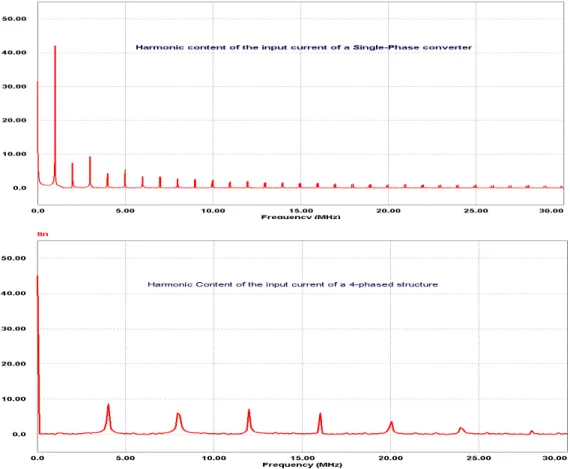
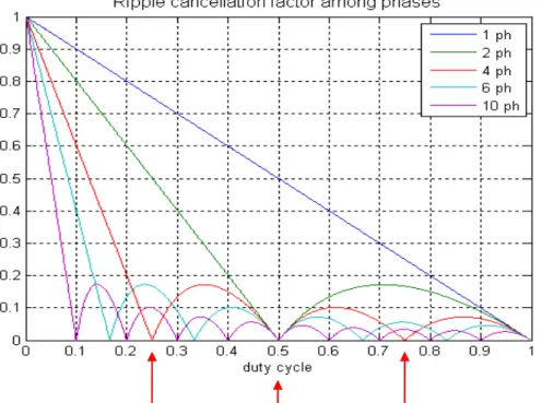
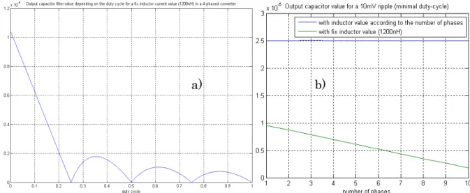
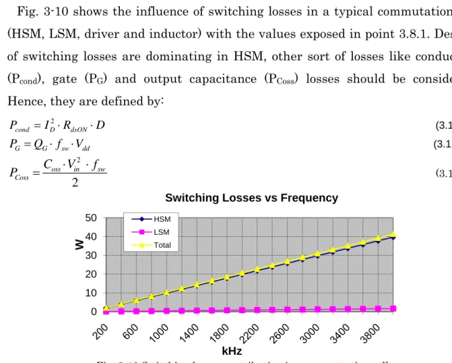
Fig. 2‐1 Typical embedded microprocessors power supply chain ... 10 Fig. 2‐2 Built‐in VRM for an Intel LGA775 socket ... 11 Fig. 2‐3 Embedded power supplies market ... 11 Fig. 2‐4 Original Moore’s law (left), Gordon E. Moore (center), and current law (right) ... 12 Fig. 2‐5 Microprocessors supply power trend ... 13 Fig. 2‐6 Power Supply architectures for PC motherboards ... 13 Fig. 2‐7 AC/DC Converter architecture. ... 15 Fig. 2‐8 Commercial AC/DC power supply ACE‐815T ... 16 Fig. 2‐9. Isolated DC/DC converters: a) Forward, b) Push‐pull c) Full‐bridge d) Half‐bridge ... 16 Fig. 2‐10 LDO regulators ... 17 Fig. 2‐11 Classical Buck converter ... 18 Fig. 2‐12 Synchronous Buck and its MOSFET circuit control ... 19 Fig. 2‐13 Multiphase synchronous Buck converter working in interleaved mode ... 20 Fig. 2‐14 Multiphase Buck converter with coupled‐inductors ... 21 Fig. 2‐15 Two‐stage Voltage Regulator ... 22 Fig. 2‐16 Multiphase Buck converter with inductive clamping system ... 23 Fig 2‐17 General block diagram for a Digital DC/DC converter ... 26 Fig 2‐18 Flash Windowed‐ADC in a digital voltage‐mode controlled Buck converter ... 28 Fig. 2‐19 Delay line ADC: simple (left) and with calibration system (right) ... 30 Fig. 2‐20 Influence of the DPWM resolution in the output voltage . ... 31 Fig. 2‐21 DPWM topologies ... 33 Fig. 2‐22 Digital design possibilities ... 34 Fig. 3‐1 Harmonic content of the input current in a Single‐Phase Synchronous and a 4‐phased converter ... 45 Fig 3‐2 Commercial inductance model ... 47 Fig 3‐3 Frequency characterization of a commercial inductance using an impedance analyzer ... 48 Fig. 3‐4 Normalized ripple cancellation factor for a n‐phased power converter depending on the duty cycle ... 49 Fig. 3‐5 Inductance value per phase). ... 49 Fig 3‐6 Frequency characterization using an impedance analyzer for different capacitor technologie ... 50 Fig. 3‐7 Capacitor value per phase . ... 51 Fig 3‐8 MOS Protections ... 53 Fig 3‐9 HSM Turn‐on waveforms ... 54 Fig. 3‐10 Switching losses contribution in a commutation cell ... 55 Fig 3‐11 Thermal image of the driver and active devices of a typical multiphase converter commutation cell .. 57 Fig 3‐12 Synchronous Buck converter with inductor DCR current sense circuit ... 60 Fig. 3‐13 Magnitude Bode Plots of the current‐sense circuit for different DCR values ... 61 Fig. 3‐14 Low.current Inductor DCR current sense example ... 62 Fig. 3‐15 Medium.current Inductor DCR current sense example ... 62Fig. 3‐16 Inductor DCR current sense example in an interleaved converter ... 63 Fig. 3‐17 Theoretical losses distribution in the power stage of the first prototype ... 64 Fig. 3‐18 Comparison of the theoretical and practical efficiency in the power stage of the first prototype ... 64 Fig. 3‐19 Power stage for the first experimental single‐phase prototype ... 65 Fig. 3‐20 Power stage for the second experimental single‐phase prototype ... 66 Fig. 3‐21 Experimental losses distribution in the power stage of the second prptotype ... 66 Fig. 3‐22 Power stage for the multiphase experimental prototype ... 67 Fig. 4‐1 Set of small signal transfer functions defining a power converter ... 72 Fig. 4‐2 Small‐signal Buck converter average model ... 73 Fig. 4‐3 Continuous‐to‐discrete time conversion of the control‐to‐output voltage small‐signal tran. function .... 74 Fig. 4‐4 State‐space variables evolution... 75 Fig. 4‐5 Small‐signal model of Digital Voltage Mode Control ... 79 Fig. 4‐6 Discrete‐time small‐signal model of Digital Voltage Mode Control ... 80 Fig. 4‐7 PID position algorithm with backward Euler approximation for the integral term. ... 82 Fig. 4‐8 Setpoint Weighting PID algorithm with backward Euler approach for the integral term. ... 83 Fig. 4‐9 PID incremental algorithm ... 83 Fig. 4‐10 PSIM and Simulink models of DVMC ... 84 Fig. 4‐11 DVMC: Simulation results for a 5A load variation ... 85 Fig. 4‐12 Pole & zero map (left) and frequency response of the loop gain. ... 86 Fig. 4‐13 Ridley’s small‐signal model for CMC ... 88 Fig. 4‐14 Continuous‐time Peak‐Current Mode Control ... 89 Fig. 4‐15 PSIM Simulation of continuous‐time Peak‐Current Mode ... 90 Fig. 4‐16 Simulink simulation of continuous‐time Peak‐Current Mode ... 90 Fig. 4‐17 Bode diagram (left) and closed‐loop pole‐zero map (right) ... 91 Fig. 4‐18 Bode diagram of the control‐to‐output voltage transfer function in CMC. ... 92 Fig. 4‐19 Small‐signal model of DCMC ... 92 Fig. 4‐20 PSIM simulation model of discrete‐time PCMC ... 93 Fig. 4‐21 Discrete‐time PCMC: Influence of the delay in the output voltage in a 5A load variation ... 93 Fig. 4‐22 Discrete‐time PCMC: Influence of the sampling frequency in the output voltage in a 5A load step ... 94 Fig. 4‐23 Discrete‐time PCMC: Influence of the sampling frequency in the output voltage in a 5A load step ... 95 Fig. 4‐24 Discrete‐time PCMC: Influence of the converter model in the output voltage in a 5A load step ... 96 Fig. 4‐25 Algorithm of adaptive duty‐cycle control law ... 97 Fig. 4‐26 Predictive control principle ... 98 Fig. 4‐27 Comparison of OCPP and DPCMC for different sampling frequencies. ... 99 Fig. 4‐28 Diagram block model of OCPC control law ... 100 Fig. 4‐29 OCPC: One‐cycle predictive control action in the duty‐cycle generation ... 100 Fig. 4‐30 OCPC simulation model ... 101 Fig. 4‐31 OCPC closed‐loop pole‐zero map ... 102 Fig. 4‐32 Simulation of valley OCPC for a 5A load step change. ... 102
Fig. 4‐33 Simulation of peak OCPC for a 5A load step change. ... 102 Fig. 4‐34 OCPC: duty‐cycle generation ... 103 Fig. 4‐35 Feedforward block diagram: IVFF (left), OCFF (right)... 104 Fig. 4‐36 Voltage Mode Controlled‐Buck with Input Voltage Feedforward ... 105 Fig. 4‐37 Open‐loop gain Bode Diagram: without IVFF (top) and with it (bottom)... 106 Fig. 4‐38 Transient response for different input‐voltages: ... 106 Fig. 4‐39 Digital OCFF loop ... 107 Fig. 4‐40 Digital Average‐Current Mode Control + OCFF for a 20A load variation... 108 Fig 4‐41 Loadline Regulation for 775_VR_CONFIG socket. ... 109 Fig. 4‐42 General schema of VMC for a n‐phased parallel power converter associated to individual ACS ... 110 Fig. 4‐43 Democratic Current Sharing using Voltage‐Mode Control for an n‐phased parallel converter ... 112 Fig. 4‐44 DCS using CMC for a n‐phased parallel with individual CS loops ... 114 Fig. 4‐45 DCS using CMC for a n‐phased parallel with common voltage compensator ... 115 Fig. 5‐1 Electrical schema of the first digtally‐controlled single‐phase power converter ... 122 Fig. 5‐2 First Experimental prototype: DSC‐controlled single‐phase synchronous Buck power converter ... 123 Fig. 5‐3 Input module (left) and its working principle (right) ... 124 Fig. 5‐4 Inductor current ADC characterization. ... 125 Fig. 5‐5 Output module working principle ... 125 Fig. 5‐6 Example of Output module for high‐frequency applications made in the LAAS ... 126 Fig. 5‐7 DVMC simulation model ... 127 Fig. 5‐8 Bode diagrams for DVMC ... 129 Fig. 5‐9 Closed‐loop gain pole‐zero map ... 129 Fig. 5‐10 DVMC: Output voltage and output current for a 5.7A load variation ... 130
Fig. 5‐11 DVMC: Steady‐state for Iout=1.8A and Vin=12V ... 131
Fig. 5‐12 DVMC: Output‐voltage ripple in steady‐state for Iout=1.8A and Vin=12V... 131
Fig. 5‐13 DVMC: 5.7A load variation, Vin=12V... 131 Fig. 5‐14 Simulink Comparison of classical DVMC and DVMC using LUT ... 132 Fig. 5‐15 Experimental Comparison of classical DVMC and DVMC using LUT ... 133 Fig. 5‐16 DVMC with IVFF for Vin=3, 5 and 12V ... 133 Fig. 5‐17 DVMC with a 15A current limitation ... 135 Fig. 5‐18 Bode diagrams for OCPC ... 136 Fig. 5‐19 Pole‐zero map for OCPC ... 136 Fig. 5‐20 OCPP simulation model ... 137 Fig. 5‐21 OCPP: Output voltage and output current for a 8A load step ... 137
Fig. 5‐22 OCPC: Steady‐state for Iout=∙3A ... 137
Fig. 5‐23 OCPC: 6.6A load variation ... 138
Fig. 5‐24 FPGA‐controlled single‐phase power converter ... 140
Fig. 5‐25 DVMC simulation model ... 142
Fig. 5‐27 DVMC: Closed‐loop pole‐zero map ... 144
Fig. 5‐28 DVMC: Output voltage and output current for a 5.7A load variation ... 144
Fig. 5‐29 DVMC: : Steady‐state for Iout=1.8A and Vin=12V ... 144
Fig. 5‐30 DVMC: Output‐voltage ripple in steady‐state for Iout=1.5A and Vin=12V... 145
Fig. 5‐31 DVMC: Output voltage and output current for a load step of 5.8A ... 145 Fig. A‐ 1 Power converter topologies depending on switch status ... 165 Fig. A‐ 2 Buck Converter switched‐model and output voltage ... 168 Fig. A‐ 3 State‐space variables evolution in discrete‐time ... 170 Fig. A‐ 4 4‐phased DC/DC converter with VMC ... 179 Fig. A‐ 5 Output voltage (left) and inductor currents (right) ... 179 Fig. A‐ 6 4‐phased DC/DC converter with Democratic Current Sharing and Voltage‐Mode Control ... 180 Fig. A‐ 7 4‐phased DC/DC converter with Democratic Current Sharing and Peak‐Current‐Mode Control ... 180 Fig. A‐ 8 4‐phased DC/DC converter with Dedicated Master‐Slave CS and Voltage‐Mode Control ... 181 Fig. A‐ 9 4‐phased DC/DC converter with Dedicated Master‐Slave CS and Current‐Mode Control ... 181 Fig. A‐ 10 4‐phased DC/DC converter with Automatic Master‐Slave CS and Voltage‐Mode Control ... 181 Fig. A‐ 11 4‐phased DC/DC converter with Automatic Master‐Slave CS and Current‐Mode Control ... 182 Fig. A‐ 12 4‐phased DC/DC converter with Interleaved Peak‐Current‐Mode Control... 182 Fig. A‐ 13 Simulations of a 4‐phased DC/DC converter with some Current‐Sharing techniques ... 183 Table 2‐1. Comparison of losses in the switch in the Buck converter ... 20 Table 2‐2 Comparison of Digital vs. Analogue controllers characterisitics ... 25 Table 2‐3 Commercial ADC summary ... 29 Table 2‐4 Comparison of digital controllers ... 36 Table 3‐1 Technical specifications for multiphase DC/DC converters ... 44 Table 3‐2 Heatsink sizing design guidelines ... 58 Table 3‐3 Values of the components for the power stage of first prototype ... 64 Table 3‐4 Theoretical maxinal losses contribution in the power stage of the first prototype) ... 64 Table 3‐5 Values of the components for the power stage of the second prototype ... 65 Table 3‐6 Values of the components for the power stage of the third prototype ... 66 Table 4‐1 Set of small signal transfer functions defining a power converter ... 72 Table 4‐2 Delay effect in the stability margins of the digitally‐controlled system ... 74 Table 4‐3 DC/DC converter specifications ... 84 Table 5‐1 Design specifications for embedded laptop microproccesors ... 122 Table 5‐2 Example of the execution time of a single instruction ... 123 Table 5‐3 Delay calculation for DVMC ... 128 Table 5‐4 Comparison of simulation and experimental performances for DVMC ... 132 Table 5‐5 OCPC: Comparison of simulation and experimental results ... 138 Table 5‐6 Comparison of simulation and experimental performances for DVMC ... 145 Table A‐ 1 State‐Space matrix for the Buck converter ... 166 Table A‐ 2. Value of the blocks in the Ridley model... 176
A
CRONYMS
L
IST
ACR: AC Resistance
ACS: Active Current-Sharing
ACMC: Average Current-Mode Control ADC: Analogue-to-Digital Converter
ASIC: Application Specific Integrated Circuit AT: Advanced Technology
ATX: Advanced Technology eXtended AVP: Adaptive Voltage Positioning CCM: Continuous Current Mode CMC: Current-Mode Control
CMOS: Complementary Metal-Oxide Semiconductor CPC: Current-Programmed Control
CPU: Central Process Unit CS: Current-Sharing
DAC: Digital-to-Analogue Converter DCM: Discontinuous Current Mode DCMC : Digital Current-Mode Control DCR: DC Resistance
DPCMC: Digital Peak Current-Mode Control DPS: Distributed Power Supply
DPWM: Digital Pulse Width Modulator DSC: Digital Signal Controller
DSP: Digital Signal Processor
DVMC: Digital Voltage-Mode Control DCS: Democratic active Current Sharing EMI: ElectroMagnetic Interference ESL: Equivalent Series Inductance ESR: Equivalent Series Resistance FF: Feedforward
FoM: Figure of Merit
FPGA : Field Programmable Gate Array HDL: Hardware Description Language HSM: High Side MOS
IC: Integrated Circuit IMC: Internal Mode Control IVFF: Input-Voltage Feedforward LDO: Low DropOut
Recherche Scientifique
LISPA: Laboratoire pour l’Intégration des Systèmes de Puissance Avancés LFM: Linear Feet per Minute
LPX : Low Profile eXtended LSB: Less Significant Byte LSM: Low Side MOS LUT: Look-Up-Table MLCC: MultiLayer Ceramic MOS: Metal Oxide Semiconductor
MOSFET: Metal Oxide Semiconductor Field Effect Transistor MS: Master–Slave
NLX: New Low profile eXtended OCFF: Output-Current Feedforward OCPC: One-Cycle Predictive Current PCMC: Peak Current-Mode Control PFC: Power Factor Correction PFM: Pulse Frequency Modulator PI: Proportional Integral
PIC: Programmable Interrupt Controller PID: Proportional Integral Derivative PIN: Positive- Intrinsic-Negative PLD: Programmable Logic Device PoL: Point-of-Load
PTC: Positive Temperature Coefficient PWM: Pulse Width Modulator
RAM: Random Access Memory ROM: Read Only Memory
SAC: Analogue-Controlled System SDC: Systems with Digital Control µc: microcontroller
µp: microprocessor VD: Voltage-Droop
VHDL: Very High-level Design Language VID: Voltage IDentification
VMC: Voltage-Mode Controlled VR: Voltage Regulator
VRD: Voltage Regulator Down VRM: Voltage Regulator Module
WTX: Workstation Technology eXtended ZOH: Zero Order Hold
Chapter 1
1.
I
NTRODUCTION
Embedded applications have emerged notably during the past few years. Actually, more and more people carry on nomad and traveler lifestyles being the cause of a considerable increase and development of portable and autonomous systems. As a consequence, energy sources, their corresponding storage devices and power management control systems should be improved substantially to obtain optimal and long-duration working modes. In view of that, new issues in the quest for a longer autonomy in embedded systems have appeared recently.
Furthermore, embedded products own strict power supplies design requirements which are becoming more and more critical with the increasing complexity of the functionalities proposed by these new portable devices.
As a matter of fact, some parameters like weight, size, robustness and cost should be taken into account to achieve efficient embedded systems. As a result, manufacturers need more compact, flexible, efficient and cheaper power supplies modules for their embedded applications.
In this context, power management discipline is becoming more and more important for the design and manufacture of embedded systems in the automotive, consumer and other industrial markets. Hence, our principal objective along the three years of this dissertation has been the study of more compact power supplies dedicated to high-current and low-voltage loads. Therefore, our aim is to introduce optimized power supply architectures and their corresponding control systems dedicated to embedded microprocessors. In view of that, a meticulous design methodology of this kind of power supply modules and their control systems has been completed in order to assure adequate robustness and fast system responses as well as enhanced efficiencies for a wide range of loads. In particular, the core of this dissertation is the study of several digital control laws which can be used in new Voltage Regulators (VR) topologies working at high switching frequencies.
Thereby and to evaluate recent advances in this sort of applications, a state-of-the-art of main power conversion architectures used in embedded systems has been developed as well as their corresponding evolutions. In response to this later report, our interest is focused on Point-of-Load (PoL) and VR architectures since
they present innovative power supply features. Nevertheless, these new topologies demand important developments to respond to future power supply requirements imposed by microprocessor manufacturers. At present, digitally-controlled multiphase power converters seems a suitable candidate for this sort of embedded power supplies. Indeed, they solve major problems of efficiency for high-current and high-frequency power supply requirements. On the other hand, digital control allows designers significant benefits due to their flexibility and their numerous possibilities of design as it is illustrated along this dissertation in different examples.
As a result, to face these new challenges in the power management field, our work takes part in the LISPA (Laboratoire pour l’Intégration des Systèmes de Puissance Avancés) project where the LAAS-CNRS and Freescale Semiconductor are associated in this new French regional (Midi-Pyrenean) collaboration. In this context, new solutions for PoL and VR applications are developed in such a way that understand better the problems and limitations of this kind of power supply architectures oriented to embedded power microprocessors.
Therefore, this dissertation has been divided in five main chapters. Thus, the second chapter introduces to the reader the work context of this dissertation and the state-of-the-art of Distributed Power Supply architectures. Then, different possibilities for digital controllers dedicated to manage power converters and their main design trade-offs are listed at the end of this chapter. Moreover, a short chronological evolution of digitally-controlled power converters is disclosed in this part.
Next, a theoretical analysis of the power stage is developed in the third chapter. Here, some technological challenges are treated in order to optimize the efficiency and the robustness of a high-current, low-voltage and high-frequency multiphase interleaved DC/DC converter.
The fourth chapter is focused on the theoretical study of the digital control laws dedicated to VRs. Thus, main control laws used in this field are modeled and adapted for this kind of applications. In addition, some guidelines are given for a correct design of a digitally-controlled DC/DC converter. Furthermore, these control laws have been illustrated in several examples in order to validate our digital control design methodology.
Our last chapter groups the studies disclosed in the previous sections. Therefore, some experimental prototypes developed during these three years are presented in this part. First practical design is based on a Single-Phase Synchronous Buck power converter controlled by a Digital Signal Controller. After, the digital controller has been replaced by a FPGA obtaining our second experimental prototype. The new digital controller allows us to beat the frequency constraints imposed by our previous experimental prototype. Finally, the Single-Phase power stage has been replaced by a multiphase architecture in our third experimental example to obtain an experimental validation of our systems at high currents. In this later prototype, a Current-Sharing control loop has been added in order to complete a full digitally-controlled multiphase DC/DC power converter. This last work will be presented in a near future and it is not included currently in this manuscript.
Chapter 2
D
ISTRIBUTED
P
OWER
S
UPPLY
A
RCHITECTURES
F
OR
E
MBEDDED
M
ICROPROCESSORS
2.
D
ISTRIBUTED
P
OWER
S
UPPLY
A
RCHITECTURES
F
OR
E
MBEDDED
M
ICROPROCESSORS
2.1
Introduction
Nowadays, power supply requirements for embedded and autonomous applications are becoming more and more severe. On one hand, the apparition of new portable electronic devices like cell phones, GPS, PDAs or MP4 represents an important challenge in terms of power autonomy. Actually, they have instigated the quest for more efficient power supply systems in order to enlarge the duration of their batteries. On the other hand, embedded processing units require higher amounts of energy due to the increasing number of transistors in this sort of devices. Thus, international standards for embedded power supply applications demand robust and compact modules which must be able to accomplish strict requirements on the conversion, transmission and level adaptation of the electrical energy.
As a result, our efforts have been focused on the study and design of power supply systems for embedded microprocessors. To illustrate and validate our purpose, the power supply system for a typical PC motherboard embedded microprocessor has been chosen as example since it owns very specific power supply requirements. However, an important part of our work is based on the theoretical development of digital control laws covering different power converters. Indeed, these control laws can be applied in a wide range of supply powers and working frequencies: from the watt (for portable applications) up to hundred of watts (telecommunication servers or automotive applications) considering frequencies over the MHz. To know exactly how a digitally-controlled power converter can be obtained, the specific parts involving this sort of systems have been investigated as wells as the different control techniques to manage properly these applications in order to find future optimal answers for current technological challenges.
Therefore, the first part of this chapter introduces the work context of this dissertation with a brief state-of-the-art of Distributed Power Supply architectures. Furthermore, a short introduction of current digital controllers
~
AC/DC VR Modules (VRM)oriented to this kind of applications as well as the chronological evolution of digitally-controlled power converters is disclosed along this section.
2.2
Evolution of power supply architectures for
embedded microprocessors
2.2.1
Work principle of Distributed Power Supply
architectures
Power conversion chain for an embedded power supply system (from the electrical grid until the load) is composed by several blocks as it can be observed in the simplified schema of Fig. 2-1. The main objective is to complete the global power conversion obtaining minimal losses. In this case a high-efficiency AC/DC converter block is found in first place. Next, a dedicated DC/DC converter which adapts power levels according to the desired supply requirements of each load.
This later block, specially conceived to supply embedded microprocessors, is known as Voltage Regulator (VR). Hence, a VR is a high-efficiency power converter which can deliver the most advantageous power level depending on the conditions required by the load (in steady and also during transient states). Consequently, VRs allow a tight and fast regulation of their output variables.
Fig. 2-1 Typical embedded microprocessors power supply chain
VRs can be divided into two main groups named VRM (Modules) and VRD (Down). The main difference between VRMs and VRDs is those later are not integrated in the motherboard design. an example of a commercial motherboard including a built-in VRM for an Intel LGA775 [2.1] socket microprocessor can be observed in Fig. 2-2.
In co embed curren supply Our m which family At pr supplie compet Micr ommercial ded produ t levels a y current le main objec can be use of product resent tim es motivat te for integ roprocessor s Output filte capacitor ba Fig. 2-2 applicati ucts. As a around 1A evels high Fi ctive is th ed as powe ts represe mes, the e tes that m grate mor socket er MLCC ank 2 Built-in VR ons, VRs an exampl A. In cont her than 10 ig. 2-3 Embe he analysis er supply ents a new endless te main micro e and mor RM for an In serve as le, current trast, typi 00A as it i edded power s and desi modules f challenge echnologic oprocessor re transist ntel LGA775 supply m t PDAs or ical deskt s illustrat r supplies m ign of high for desktop e for Frees cal evoluti rs manufa tors in a lo 5 socket module for r cell pho top or ser ted in Fig. arket h-current V p PC micro scale Semi ion of thi acturers lik ower silico a wide ra ones need rver PCs 2-3. VR archit oprocessor iconductor is kind of ke Intel o n surface. VRM ange of supply require tectures rs. This r. f power or AMD
Furthermore, new built-in transistors should work at higher switching frequencies to boost the microprocessor power calculation. However, the increasing trend of the number of transistors as long as the computers progress was predicted already by Gordon E. Moore in 1965. Thus, the Moore’s law (see Fig. 2-4) enunciates that the number of transistors per inch in a processor is duplicated each 2 years in order to reply their continuous progress [2.2] . As a result, the microprocessor power supply demands are constantly increasing.
Fig. 2-4 Original Moore’s law (left), Gordon E. Moore (center), and current law (right)
In particular, the evolution of present lithographical process requires supply voltages around 1V. In consequence, the foremost trend is to reduce the supply voltage level delivered to the microprocessor to limit the electrical field inside the silicon chip. Actually, as long the lithographical process values are decreased, the voltage supply levels delivered to the IC should be reduced correspondingly.
Anyway, this value will be decreased in the near future as it can be seen in Fig. 2-5. However, this droop in the supply voltage levels is not costless. As a matter of fact, the evident consequence is that supply current levels must be increased in order to deliver to the load a constant supply power [2.3] .
Fig. 2-5 Microprocessors supply power trend
Considering previous supply power requirements, current desktop computers require high efficiency, high power density, high reliability and fast transient responses In the past, a typical power supply system was constituted by a single module adapting AC levels into a large range of DC values (see Fig. 2-6 a).
Fig. 2-6 Power Supply architectures for PC motherboard: a) centralized, b) distributed topology for telecom and server PCs, c) distributed topology to desktop and laptop PC
a) b) c) 0 10 20 30 40 50 60 70 80 90 100 20 05 20 06 20 07 20 08 20 09 20 10 20 11 20 12 20 13 20 14 20 15 20 16 20 17 20 18 20 19 20 20 (nn) 0 0,2 0,4 0,6 0,8 1 1,2 (V ) lithography vcc
This single module was called ‘Silver Box’ due to its sheet-metal enclosure. It presented a high consumption due to the large supply power range which should deliver to the different loads of the embedded system. In essence, the efficiency of the conversion block was reduced significantly because of the inductive and resistive parasitic effects produced by the connections between the Silver Box and the microprocessor. Furthermore, the Silver Box was not able to deliver the most convenient supply levels for each load. This was due to its single AC/DC conversion structure which was neither flexible nor well-adapted for several load requirements.
Thereby, classical centralized power supplies were replaced for more efficient Distributed Power Supply architectures (see Fig 2-6 b and c). Indeed, Distributed Power Supply topologies offer important advantages in terms of efficiency, power density and power matching. As a result, losses are appreciably reduced as well as thermal effects. Thus, these power supply structures are constituted by several conversion blocks.
As it can be observed in Fig. 2-6, two conversion principles can be choosen to assure appropriate power levels in the embedded microprocessors supply chain. Therefore, it can be selected either one schema or the other depending on our technical requirements. First chain presented in Fig. 2-6b is found often in networks and telecommunication applications where supply power is important.
In these cases, AC signals (115VAC or 230VAC) are transformed initially into high DC levels by means of an independent bulk AC/DC converter. In spite of 48V is the typical DC value, the telecom range works properly in the 36-75V range. Anyway, the European standards reduce the maximal value to 60V. After the AC/DC conversion, an isolated DC-DC step-down converter transforms the 48V to lower DC levels (typically 12V). These intermediate DC levels are transmitted to a common bus. Typically, isolation is needed to protect the system from dangerous spikes and to prevent ground-loops as well.
On the other hand, typical supplies for desktop or laptop computers are presented in the previous schema (see Fig. 2-6 c). In most of cases, the isolation stage is not necessary. Moreover, for embedded applications, the suppression of this protection implies a reduction of the weight and cost. After, a second non-isolated DC/DC converter completes the voltage level adaptation to the desired
one by the common bus (12V typically) optimizing the global power matching, Concerning the AC/DC stage, it must assure PFC (Power Factor Correction) role associated to an isolation block (typically a transformer, see Fig. 2-7). Hence, the PFC circuit is used to decrease the harmonic content and to accomplish with some standard requirements (e.g. IEC1000-3-2 or EN 61000-2-3).
Previous block is based classically on a Boost converter configuration with variable regulation depending on the converter conduction mode (CCM or DCM). Thus, the primary stage of the transformer is typically composed by a Forward or a Bridge (half or full) topology depending on the expected power requirements. In the secondary stage of the transformer, Schottky diodes or low-voltage MOSFETs switches (in a synchronous regulation) are found typically to complete the AC/DC transformation.
Fig. 2-7 AC/DC Converter architecture.
Some AC/DC systems, which are normally destined to server computers in critical applications, incorporate parallel auxiliary systems to have redundant supply systems in case of failure. These systems are known like “ORing” and they are composed by either Schottky diodes or MOSFET [2.4] . An example of a commercial AC/DC system and its associated technical characteristics is illustrated in Fig. 2-8 [2.5] .
An isolated DC/DC converter is required in telecom and server applications, i.e. like in all applications connected to the electrical grid.
Fig. 2-8 Commercial AC/DC power supply ACE-815T
This converter does not need a tight output regulation because load requirements are not critical. Forward, Push-Pull and Bridge topologies are the most common choices as it is represented in Fig. 2-9.
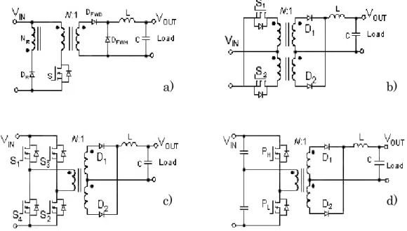
Fig. 2-9. Isolated DC/DC converters: a) Forward, b) Push-pull c) Full-bridge d) Half-bridge
Following the supply chain, the intermediate common bus voltage carries the power levels until different non-isolated switched DC/DC converters known as Point-of-Load (PoL) and/or VR converters. PoL converters are placed as near as possible to their corresponding load completing more efficiently the power transmission and conversion. Moreover, PoLs are used to provide a low and tight regulated DC voltage to the load from the intermediate voltage bus or from the battery. Furthermore, PoLs reduce considerably distribution losses obtaining important benefits like enhanced power matching, high efficiencies and saving space and money as well. Moreover, for applications needing high-powers, PoLs
Power Supply Type AC-DC with PFC Power Supply Standard AT
AC Input Voltage 115, 230 V DC Output Voltage +5V +12V -12V DC Output Current 14A 4.2A 0.3A
Output Power: 150 W
Efficiency 65% Dimensions 150x81.5x40.5mm
a) b)
also can be used in parallel structures offering high current levels without over-sizing active and passive system devices.
Simultaneously, VRs are used to supply the built-in microprocessors of the motherboards following some industrial standards like ATX, FlexATX, microATX, AT, LPX, NLX, and WTX. Each one of these standards corresponds to different power supply requirements [2.6]
By and large, the global efficiency and the power-matching of the system are improved for a wide range of loads thanks to VR and PoL converters. For that matter, these power converter architectures have been chosen to develop new digital control algorithms for our experimental implementations.
2.2.2
Point-of-Load and Voltage Regulator
architectures
2.2.2.1 Introduction
Two main conversion principles which give place to two complementary families of commercial products are found in PoL and VRs applications. First family is composed by LDO (Low DropOut) linear regulator and the second one consists of switching converters.
Fig. 2-10 LDO regulators
LDO regulators are used when input and output voltages are near similar. If this condition is not accomplished, their efficiency is punished drastically. LDO are exclusively step-down architectures implying that output voltages values are always lower than input ones. Their main advantages are their simple control (regulation can be achieved easily with a high accuracy) and their good harmonic generation, especially in high-frequency applications. Moreover, they deliver very low ripple values to the load. Nevertheless, these structures are less used
nowadays as embedded power supplies due to its poor efficiency and its important size and weight. Two examples of LDO are represented in previous Fig. 2-10.
To solve the efficiency problem inherent to LDO structures, switching converters have replaced progressively these linear converters during the past few years. Switching converters offers a higher efficiency despite of their more complicate control system. For PoL and VR applications, the Buck converter is the most widespread choice. The Buck converter offers several benefits like good efficiency, easy control and a good stability associated to its minimal-phase behavior. Therefore, the Buck converter represents the basic DC/DC power conversion block and it is described in detail in next sections.
2.2.2.2 The classical Buck Converter
Nowadays, the step-down Buck structure is the widest topology employed in PoL and VRM converters. However, some variations of the classical structure are found to improve the power efficiency. Basically, these variations are introduced in such a way to reduce losses in the active devices. The basic configuration involves one controlled-switch associated to a non-controlled one (freewheeling diode) as it can be seen in Fig. 2-11.
Fig. 2-11 Classical Buck converter
This configuration has considerable conduction losses due to the diode Forward voltage (Vd). As a matter of fact, DC/DC converters delivering low-output voltages to the load own high conversion rates and, therefore, they have small duty-cycles in steady-state. Consequently, the ON-state time of the freewheeling diode is augmented drastically increasing conduction losses and reducing the system efficiency correspondingly. As a result, the classical Buck converter is not recommended for embedded applications.
VL Vd Vout
As a used in describ 2.2 The configu low-pow pendin to the c This High-S MOS (L The g Howev corresp switchi (known control As a and ex and its among Table using examp a conseque n VR app bed in next 2.2.3 Th losses pro uration ca wer applic ng its ON-conduction topology Side MOS LSM, SW2 global beh ver, both ponding co ing period n as “dea l signals o consequen xpensive th s control g efficiency F e 2-1 show the Sync le, an exa ence, more plications. t points. he Synch oblem cau an be redu cations, a -state. Con n resistanc called Sy (HSM, SW 2) as it is i havior of th MOS sho onduction ds. To avoi adtime”, se f both MO nce, the s han the cl system. T y, complex Fig. 2-12 Syn ws a num chronous ample usin e optimal The mos hronous used by th uced replac MOSFET nsequently ce of both ynchronou W1) associ illustrated his configu ould work times to id both sw ee Fig. 2-OS. yncrhonou lassical on Thus, for ity and co nchronous B merical exa Buck con ng a volta architectu st widespr Buck co he freewh cing this d T is chosen y, conduct active swi us Buck o ated to a s d in Fig. 2-uration is k in a com avoid des witches sim -12) is int us Buck a ne due to t embedded st.
Buck and its
ample of t nfiguration age conve ures based read archi onverter heeling di device by n normally tion losses itches. wns a po synchrono -12. quite simi mplement structive s multaneou troduced architectur the additi d applicat MOSFET c the gain i n for a lo rsion from d on the cl itectures u r ode of th a second y due its r s are dire ower activ ous device ilar than t tary way short-circu us conduct in-betwee re is a litt on of the tions, a tr circuit contro in the con ow-power m 5-to1V r lassical Bu used in V e classica active swi resistive be ectly propo ve switch named Lo the previo respectin uits durin ion, a tim en the act tle more c second MO rade-off is ol nverter eff supply. I ratio, i.e. uck are VRs are al Buck itch. In ehavior ortional named ow-Side ous one. g their ng their me delay tivation complex OSFET s made ficiency In this a duty
a)
b)
cycle of 0.2 and delivering 20A to the load is presented. In the classical case, a Schottky diode with a very low Forward voltage (compared to a classical PIN diode where Vd>1V) is choosen. For the synchronous case, a MOSFET with minimal conduction resistance has been selected. Thus, the losses reduction obtained using the synchronous configuration can be observed in this example.
Table 2-1. Comparison of losses in the switch in the Buck converter
2.2.2.4 The Multiphase Synchronous Buck converter
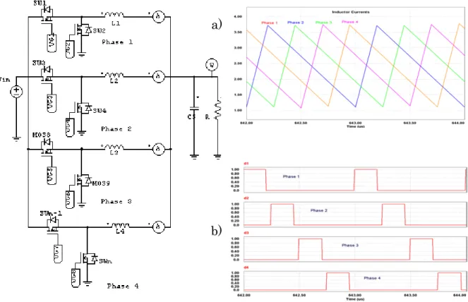
Synchronous topologies are preferred in low-voltage, high-current VR designs due to their enhanced efficiency. Nevertheless, supply requirements of new generation of embedded microprocessors cannot be covered efficiently by single-phase synchronous topologies. As a result, multisingle-phase or parallel converters (see Fig. 2-13) were born to achieve these new power supply necessities.
Fig. 2-13 Multiphase synchronous Buck converter working in interleaved mode: a) Inductor current per phase, b) duty-cycle per phase
Theoretical switch losses Numerical example Classical PD =VD·(1−D)·IL PD =0.38·(1 0.2)·20 6.08− = W
Synchronous PSW =Rds·(1−D I)· L2 PSW =0.0026·(1 0.2)·20− 2 =0.83W
Extract of datasheet specifications
Schottky Diode, IRF42CTQ030PbF : Vd=0.38V at Id=20A, Tj = 125C
MOSFET IRF6609: RdsON = 2.6mΩ at VGS = 4.5V, ID = 25A [2.6]
Then, multiphase converters allow us an important increase of the output current delivered to the load without an excessive over-sizing of the active and passive components of the power converter.
Multiphase converters are composed by basic commutation cells or phases placed in parallel as it is shown in Fig. 2-13. Each phase is activated consecutively after the previous one in an interleaving mode, i.e. with a given time interval corresponding to the number of phases of the power converter. This interleaved operation mode reduces considerably output-voltage and input-current ripples and, consequently, converter losses too. Hence, this time interval or phase-shift is defined by (2.1):
360º Phase shift (°) =
number of phases (2.1)
However, multiphase architectures still present some efficiency droops. This lack of efficiency can be minimized adding some changes to the architecture presented in this point.
2.2.2.5 Modifications in the Multiphase architecture
Multiphase synchronous Buck topologies working in interleaving mode have become an interesting option for VRs thanks to their easy design. Nevertheless, this architecture may become inefficient for large conversion ratios owning very low duty-cycles are used (e.g. 12-to-1V). In fact, low duty-cycles induce large inductor current ripples and, therefore, higher switching constraints. These constraints are translated in important switching and conduction losses in the active devices.
Fig. 2-14 Multiphase Buck converter with coupled-inductors
Therefore, other structures based on the multiphase synchronous Buck try to improve the converter efficiency and to answer to the exigent work environments
of new VR applications. In general, most of variations in the multiphase architecture serve to enlarge the converter duty-cycle reducing converter losses.
The simpler modification is presented in [2.7] [2.8] where classical inductors are replaced for coupled-inductors structures as it is illustrated in previous Fig. 2-14. However, this variation engages several drawbacks. Firstly, the increase of the number of turns limits the inductor current slew-rate. Moreover, the inevitable leakage inductance existing between both coupled windings causes voltage spikes that may damage active switches or instigate some additional losses. To reduce these spikes, a clamping circuit is added and additional filters are used to smooth inductor currents. In brief, this new architecture becomes quite complicated although some gain in the converter efficiency can be obtained.
Another approach is introduced in [2.9] with the development of a two-stage conversion system as it can be observed in Fig. 2-15. In this work, a high-efficiency, two-phased DC/DC converter makes an initial 12-to-5V conversion. Next, a second high-frequency and high-efficiency multiphase converter completes the conversion from 5-to-1V. In this design, the cost and complexity of the final system is increased widely due to the duplication of the elements of the system. Moreover, the second converter needs a very narrow regulation control system. However, the global efficiency is augmented significantly.
Fig. 2-15 Two-stage Voltage Regulator
In [2.10] a multiphase converter associated to an inductive clamping system is presented (see Fig. 2-16). In this work, authors improve the dynamical behavior of the converter during load transients using the “critical inductance” concept [2.11] . This theory calculates the maximal inductor value which gives the fastest transient response without compromising the efficiency. Thus, for inductor values larger than the critical one, efficiency and dynamical responses cannot be improved.
~
AC/DC DC/DC 48-to-12V Two-phased Buck 12-to-5V DC/DCIntermediate Bus Voltage 2-stage multiphase Buck converter
Four-phased Buck 5-to-1V
Therefore, the clamping system varies the inductance value per phase of the multiphase converter to be always under this critical value. In this context, authors force the output voltage to the desired working point. This point is calculated depending on the maximal output-voltage ripple and the maximal load current variation. Actually, this method is a variation of the Adaptive Voltage Positioning (AVP). However, the value of the inductances using this technique is extremely reduced. Hence, switching frequency should be very high to decrease inductance current ripple and to reduce conduction losses as well. Then, a trade-off between conduction and switching losses is present.
Fig. 2-16 Multiphase Buck converter with inductive clamping system
To sum up, the high supply-current needed by the new generation of embedded microprocessors is obtained thanks to more complex structures with enhanced efficiencies although new more complicate and accurate control techniques are also necessary. In this context, a lot of technological troubles associated to their power structure, their robustness, their corresponding control technique and their accuracy still have not a clear solution.
Therefore, our work methodology consists in a systematic elaboration of digital control laws and their corresponding validation in experimental prototypes. For this reason, the work elaborated during the past few years have required the simultaneous design of the parts concerning a full digitally-controlled multiphase synchronous power converter, i.e. the power stage, the digital controller and the interfaces between power and control boards.
As a result, the multiphase synchronous Buck converter working in interleaved mode has been selected because its behavior is relatively well-known. Thus, our efforts have been focused on the development of performing control algorithms
adapted to a wide range of loads. For that matter, a state-of-the-art of the different parts involving PoL and VR converters is presented in the following section. Moreover, the pros and contras of present current manufactured solutions are disclosed as well as their associated digital control laws.
2.3
State-of-the-art and Evolution of Digital
Technologies applied in Embedded Power Supplies
2.3.1
Introduction
Systems owning Digital Control (SDC) offer important advantages versus Analogue-Controlled Systems (SAC). Actually, new commercial designs point towards full-digital architectures replacing current SAC.
Indeed, SDC has lower (or comparable at least) power consumption than SAC thanks to the decreasing scaling in CMOS technologies. Moreover, the number of components in SDC is reduced drastically, then; injurious effects originated by external parameters like changes in the environment temperature, white noises, tolerances of the components or changes in the manufacturing procedures are reduced significantly. This later skill of SDC implies an important increase of the reliability of the system and, therefore, the Mean Time Before Failure (MTBF).
In SDC, integration density is increasing constantly. Then, more functions can be included in the SDC allowing designers to implement less conservative digital control laws. After that, non-linear control techniques which are nowadays unfeasible using analogue controllers can be implemented.
Concerning to multiphase systems, SDC permits a fine synchronization of their duty-cycles. This skill is very useful when the number of phases is high.
In terms of design, HDL techniques allows designer lower design times and higher flexibility to changes in their final applications. Therefore, development costs and implementation times (less Time to Market) are reduced. This is particularly important when environmental conditions of the system are often changed. In this case, new hardware configurations are not necessary implying a reduction of the final surface and cost. As an example, the traditional passive components of the analogue calibration system can be eliminated and replaced for a digital re-programmable regulation. Thus, the re-programmability of SDC
by means of changes in the software code and their high adaptation to different applications make them very practical in industrial applications.
Nevertheless, SDC hold several disadvantages and some technological frontiers still persists in these new digital controllers. Firstly, changes in the environment temperature may still cause mismatches in several devices of SDC like the clock system, the voltage reference or the ADC (Analogue-to-Digital converter). In second place, state-of-the-art digital controllers still do not own the performances enough to replaces analogue controllers. This later issue is especially important in very high-frequency applications due to time constraints. As a result, these time limitations are reflected in a drastic reduction of the bandwidth of the system because of inherent delays of the algorithm and the digital structure.
Moreover, the accuracy of the control system will be fixed by the SDC resolution. In fact, SDC resolution is given by both of ADC and DPWM (Digital Pulse Width Modulator) devices. As a result, to obtain a high-resolution ADC and DPWM involves developing large, complex and expensive structures. Additionally, to work with high-resolution devices engage an increase of the clock frequency of the DPWM and the sampling frequency of the ADC correspondingly. As a consequence, their power consumption and their cost are augmented too. Table 2-2 summarizes the pros and contras of using SDC instead of SAC.
Table 2-2 Comparison of Digital vs. Analogue controllers characterisitics
Thus, our main aim is to replace the classical analogue control stage for a digital controller which satisfies the advantages exposed in previous paragraphs. Hence, a digitally-controlled DC/DC converter can be divided in different parts as it can be observed in Fig. 2-17.
The first part corresponds to the power stage followed by the input or acquisition module. In this second stage, state-space variables of the converter are digitalized to be useful for the control stage. The third block is composed by
Skill Digital Analogue Power consumption Lower Higher
Robustness against tolerances Higher Lower
Robustness against delays Lower Higher
Flexibility Higher Lower
Time-to-market Lower Higher
Robustness against failures Higher Lower
Communications with other devices Higher Lower
the dig module power There control microp of this techno