TH `ESE
TH `ESE
En vue de l’obtention du
DOCTORAT DE L’UNIVERSIT´E DE TOULOUSE
D´elivr´e par : l’Universit´e Toulouse 3 Paul Sabatier (UT3 Paul Sabatier)
Pr´esent´ee et soutenue le 08/12/2017 par : Roberta RUFFILLI
Modes de fatigue des m´etallisations `a base d’aluminium dans les composants MOSFET de puissance
Fatigue mechanisms in Al-based metallizations in power MOSFETs
JURY
Mauro CIAPPA ETH, Zurich Rapporteur
Josef LUTZ TU, Chemnitz Rapporteur
Marie-Laure LOCATELLI Laboratoire LAPLACE, Toulouse Membre du Jury Michael NELHIEBEL K.A.I - Infineon, Villach Membre du Jury St´ephane LEFEBVRE SATIE - ENS, Cachan Membre du Jury Mounira BERKANI SATIE - ENS, Cachan Directrice de Th`ese Marc LEGROS CEMES - CNRS, Toulouse Directeur de Th`ese
´Ecole doctorale et sp´ecialit´e :
SDM : Physique de la mati`ere - CO090
Unit´e de Recherche :
This thesis, a collaboration between CEMES-CNRS, Satie laboratory (ENS Cachan) and NXP Semiconductors is motivated by the comprehension of the failure mechanisms of low voltage power MOSFET devices produced for ap-plications in the automotive industry.
A limiting factor for the long-term reliability of power modules is the electro-thermal and/or thermo-mechanical aging of the metallic parts of the source: Al metallization and bonding wires. At the temperature reached during the on-off operating cycles (few hundred degrees), the difference in the coefficient of thermal expansion between the metallization and the oxide and semicon-ductor parts induces an inevitable plastic deformation in the metal, which is the softest material in the complex MOSFET architecture.
We have characterized the metal microstructure before and after accelerated electro-thermal aging tests, by using specific techniques from the field of the physical metallurgy: electron and ion microscopy, grain orientation and chem-ical composition mapping. For the first time the source metallization has been characterized both away and under the bonding connections, which are one hundred times thicker than the metallization layer. The latter is a critical loca-tion for the reliability assessment because the ultrasonic bonding process may weaken the initial metallization microstructure by adding an important plas-tic deformation prior to aging. This is, however, poorly stated in the literature because of the difficulty to access the metallization under the wires without damaging their bonding, which is known to be particularly weak in case of aged modules.
In order to investigate the wire-metallization interface, we have set up origi-nal sample preparations, based on ion polishing, that allowed us to disclose the metallization under the bonding wires without introducing preparation artifacts in the microstructure. The bonding process induces a severe and non-uniform plastic deformation in the metallization under the wires without re-creating a good electrical contact: small cavities and native oxide residues, have been systematically observed at the Al/Al interface, in all the analyzed mod-ules, before and after aging.
The main mechanism behind the device failure is the generation and propa-gation of fatigue cracks in the aluminum metallization, associated to a local Al oxidation that prevents these crack from closing. Away and under the wire bonds, they run perpendicularly from the surface down to the silicon substrate following the grain boundaries, due to an enhanced intergranular diffusion of
sess the aging of the metal parts of MOSFET devices. The full characterization of the intrinsically defective interface generated by the bonding process and the metallization degradation during electro-thermal aging indicated paths to possible improvements of current technologies and potential developments of new processes.
Cette thèse, effectuée en collaboration entre le CEMES-CNRS, le laboratoire Satie (ENS Cachan) et NXP Semiconductors est motivée par la compréhension des mécanismes de défaillance des dispositifs MOSFET pour les applications dans l’industrie automobile.
Un facteur limitant de la fiabilité à long terme des modules de puissance basse tension est le vieillissement électrothermique et/ou thermo-mécanique des par-ties métalliques de la source: métallisation en aluminium (ou alliage) et fils de connexion. A cause de la différence de coefficient de dilatation thermique en-tre la métallisation les oxydes et le substrat semi-conducteur, la température atteinte pendant les cycles de fonctionnement (quelques centaines de degrés), induit une déformation plastique inévitable dans le métal, qui est le matériau le plus mou dans l’architecture complexe du MOSFET.
Nous avons caractérisé la microstructure métallique avant et après les tests de vieillissement électrothermique accélérés, en utilisant des techniques spéci-fiques du domaine de la métallurgie physique: microscopie électronique et ion-ique, cartographie d’orientation de grains et de la composition chimique. Pour la première fois, la métallisation de la source a été caractérisée sous les fils de connexion, qui sont cent fois plus épais que la métallisation. Cet emplace-ment est critique pour la fiabilité du composant, car le processus de soudure par ultrasons induit une déformation plastique importante qui peut affaiblir la métallisation initiale avant le vieillissement. Ceci est peu étudié dans la lit-térature en raison de la difficulté à accéder à la métallisation sous les fils sans altérer leur interface, souvent endommagée et fragilisée dans les modules vieil-lis.
Nous avons mis en place des méthodes de préparation d’échantillon, basées sur le polissage ionique, pour étudier cette interface, sans introduire d’artefacts de préparation. Le processus de soudure à froid induit une déformation plas-tique sévère et non uniforme dans la métallisation sous les fils sans parvenir à recréer un bon contact électrique: de petites cavités et des résidus d’oxyde natif, ont été systématiquement observés à l’interface Al / Al, dans tous les modules analysés, avant et après vieillissement.
Le mécanisme principal de défaillance des modules est la génération et la propagation de fissures de fatigue dans l’aluminium, associée à une oxydation locale qui empêche la fermeture de ces fissures. Sous et en dehors des fils de connexion, ces fissures traversent la métallisation perpendiculairement à la surface jusqu’au substrat en silicium en suivant les joints de grains. Cette
lissement jusqu’à l’échec.
Cette étude a établi de nouvelles techniques dédiées et des méthodes de quan-tification pour évaluer le vieillissement des parties métalliques des modules MOSFET. La caractérisation complète de l’interface soudée, intrinsèquement défectueuse et la dégradation de la métallisation pendant le vieillissement électrothermique ouvrent la voie à l’amélioration possible les technologies actuelles et au développement potentiel de nouveaux procédés.
I had the chance to do my phd at the CEMES laboratory and NXP Semicon-ductors thanks to an e-mail sent by Andrea Falqui, the head of the laboratory where I worked in Italy, to the former director of the CEMES, Alain Claverie. I have to thank Andrea to have supported my desire to progress, and Alain Claverie to put me in contact with my PhD supervisor, Marc Legros.
When I moved to Toulouse for the first time I only knew all the things I was leaving in Italy, I was scared of my first job experience abroad, I did not speak French...and I had never eaten duck in my life! Despite these (huge!) cultural gaps, it took me really a short time to find my routine in the lab...and day after day with my grains of aluminum, FIB and TEM sessions, time flew and gave me good experiences, satisfaction and new friends. And I have many people to thank for this.
First of all my supervisor, Marc Legros. It is rare to meet a person so kind, fun, respectful and competent at the same time. Despite his booked agenda, he has always found the time for me, for our experiments, for answering my questions...And for encouraging me during my peaks of stress and lack of self-confidence (sorry for this!). It has been fundamental to me his support when I thought that my little pause in the middle of my PhD could prevent me from doing a good job. He taught me many things, while letting me be independent, and I am really grateful for this. I will miss him a lot.
Thanks also to Philippe Dupuy, my co-supervisor at NXP. I have peppered him with questions during these years, in person, by sms, telephone calls...He was always available to answer, and he helped me to build my network at NXP. In this regard, I would like to thank also Yann Weber, Thomas Mazeaud and Marine de Reviers for the useful discussions. And thanks to Thomas Zirilli for the help during my first ANADEF workshop and for welcoming me in his laboratory with all his staff: Céline, Thomas, Mathias, Patrick...
I also had the chance to collaborate with the SATIE laboratory in Cachan, under the supervision of Mounira Berkani: I would like to thank her, Stéphane Lefebvre and Gilles Rostaing for welcoming me during my stays there and explaining me in a simple way the secrets of electronics and aging tests!...And for the possibility to spend four beautiful days at the University of Naples, hosted by Michele Riccio.
The cross-polisher preparations of Claudie Josse at the Raimond Castaing Center helped me to save a lot of time (sorry FIB!) during the last months of my PhD. Thank you, Claudie, for these preparations and the useful advice.
our coffee breaks speaking about the illnesses of our children! Jean-Philippe, thank you for cleaning the coffee machine every day...! And Lise, thank you for your constant self-confidence training.
During these years, I have had also difficult days and sometimes it seemed me impossible to get to the end of my PhD. In these moments, my “PhD mates” have supported me and I have never felt alone. They are really precious to me and I am proud to say that I have found good friends. I think to Thomas and Zofia, my first collègues de bureau, Chloé, Victor, Paul, Aurelie, Lionel, who had the patience to listen to my first French sentences without laughing (too much) and helped me integrating in the lab. And to all my new friends with whom I shared my choices, joy and troubles: Winnie and Soumaya, thank your for your compliments, the daydreams about our future lives and to remind me when I had to go pick up Marta! And my chers garçons: Alessandro, Arthur, Nico (thank you for waiting for me at lunch!), Élie, Max and David. Melvyn, Ségolèn, Mia, Guillaume, I am sad we have spent such a short time together.
It has been a pleasure to go to work and learn something new every day. I am really grateful for these years and I will miss them.
And to conclude, thanks to Andrea and Marta for their support and patience, especially during the preparation of the dissertation. We did a great team-work in the last years: my efforts are for you, I hope you are proud of me.
1 introduction 1
2 power electronics for the automotive industry, failure
mode... 5
2.1 Power electronics technology evolution . . . 7
2.1.1 Bipolar transistor . . . 7
2.1.2 Thyristor . . . 10
2.1.3 MOSFET transistor . . . 12
2.1.4 IGBT transistor . . . 14
2.1.5 Recent solutions: trench technology . . . 14
2.1.5.1 Vertical MOSFET . . . 15
2.1.5.2 Trench MOSFET . . . 16
2.2 Smart Power MOSFET for the automotive industry . . . 18
2.2.1 Stress conditions in power electronics for automotive . . . 20
2.2.1.1 Thermal stress . . . 20
2.2.1.2 Electromagnetic stress . . . 21
2.2.1.3 Mechanical and chemical stress . . . 21
2.2.2 Failure modes in power MOSFETs . . . 21
2.2.2.1 Die/substrate solder joints fatigue . . . 24
2.2.2.2 Failure modes in the active zone . . . 25
2.2.3 Thermosensitive aging indicators . . . 29
2.2.3.1 RDS(on) . . . 29
2.2.4 Devices under test: 45V and 65V LFET1T technology . . . 31
2.3 Reliability assessment of LFET1T power devices . . . 34
2.3.1 Test NXP . . . 39
2.3.1.1 Electro-thermal test bench . . . 39
2.3.1.2 Electro-thermal test conditions . . . 39
2.3.2 Test Satie Laboratory . . . 43
2.3.2.1 Electro-thermal test bench . . . 43
2.3.2.2 Electro-thermal test conditions . . . 45
2.3.2.3 Supplementary characterizations . . . 45
3 microstructural characterization 51 3.1 Package decapsulation . . . 52
3.2 Surface analysis . . . 54
3.2.1 Scanning Electron Microscopy and Energy Dispersive X-Ray Spectroscopy . . . 54
3.2.2 Electron Backscattered Diffraction . . . 55
3.3 Bulk cross-sectional analysis . . . 59
3.3.2.2 SEM, SIM and EDX analysis . . . 69
3.3.3 Focused ion beam tomography . . . 71
3.4 Finer cross-sectional analysis . . . 74
3.4.1 TEM lamella preparation by FIB . . . 76
3.4.1.1 Why we used the FIB . . . 76
3.4.1.2 Sample preparation protocol . . . 78
3.4.1.3 Lamella preparation at the wire-metal interface . 82 3.4.2 TEM techniques . . . 83
3.4.2.1 Automated Crystal Orientation Mapping . . . . 83
3.4.2.2 Chemical Analysis: EDX and EELS . . . 86
3.4.2.3 In situ heating experiment . . . 88
4 results 89 4.1 Aging of SPD06 components . . . 91
4.1.1 Topographical study . . . 91
4.1.1.1 As-is metallization microstructure . . . 93
4.1.1.2 Aged metallization microstructure . . . 93
4.1.2 Cross-sectional study . . . 98
4.1.2.1 Naked metallization . . . 98
4.1.2.2 Metallization under the bonding wire . . . 101
4.1.3 Temperature cycles: TEM heating in situ experiments . . . 105
4.2 Aging of T07D17 components . . . 108
4.2.1 Naked metallization cross-sectional study . . . 111
4.2.1.1 Cracks propagation statistics . . . 115
4.2.1.2 Cracks propagation under the passivation layer . 116 4.2.2 Metallization under the bonding wire . . . 120
4.2.2.1 Wire-metallization interface . . . 121
4.2.2.2 Plastic deformation due to the bonding process - Statistics . . . 125
4.2.3 In depth investigation of the whole wire-metallization in-terface by Cross Polisher preparation . . . 130
4.2.3.1 Plastic deformation of the initial metallization under the bonding wire . . . 133
4.2.3.2 Crack propagation in the metal and semicon-ductor of the aged modules . . . 136
5 discussion 147
5.1 Rds(on)evolution during electro-thermal aging . . . 148
5.1.1 Potential and temperature mapping . . . 148
5.2 Source metallization reconstruction and crack propagation . . . . 152
5.2.1 Possible deformation mechanisms . . . 155
5.2.2 Plasticity by dislocation propagation . . . 157
5.2.3 Plasticity by atom diffusion . . . 158
5.2.4 Plasticity by electromigration . . . 161
5.2.5 Fatigue crack propagation: SPD06 vs T07D17 . . . 162
5.2.6 Passivation and temperature effect on crack propagation . 164 5.3 Weakening of the bonding connections . . . 167
5.3.1 Initial wire-metallization interface . . . 168
5.3.2 Initial Plastic deformation . . . 171
5.3.3 Aging in the metallization under the bonding wires . . . 173
5.3.4 Crack propagation during electro-thermal aging . . . 173
6 conclusion and perspectives 177 i appendix 183 a conventional cross-section tem sample preparation 185 b curvature experiment 189 ii résumé étendu 195 c modes de fatigue des métallisation à base d’aluminium...197
c.1 introduction et objectifs . . . 197
c.2 Technologie LFET1T et vieillissement accéléré des composants . 198 c.2.1 Technologie LFET1T . . . 199
c.2.2 Tests de vieillisssement accéléré . . . 199
c.3 Techniques expérimentales de characterization microstructurelle de la métallisation . . . 200
c.4 Etude du vieillissement de la metallisation et des fils de connextion203 c.4.1 Métallisation nue (hors zone de bonding) . . . 205
c.4.2 Interface métallisation / fils . . . 211
c.5 Fissuration dans le semiconducteur . . . 212
c.6 Conclusions et perspectives . . . 216
• Fatigue mechanisms
• Wire-metallization interface
• Metallization microstructure aging • Electron microscopy
• Ion microscopy
• Grain structure mapping
1
I N T R O D U C T I O N
Over the last few decades, the automotive industry has started to progressively replace electro-mechanical components by purely electronic devices or minia-turized electro-mechanical systems based on Si-technologies. This paradigm shift has initially involved support electronic systems (e.g. ABS, power-assisted steering, speed limiter, air conditioning, etc.). However, the constant technol-ogy evolution and miniaturization have rapidly broadened the field of appli-cation of electronics in automotive, involving the main vehicle functions (e.g. propulsion, lighting, brakes, engine, fan control, battery management etc.) and increasingly replacing the conventional mechanical and hydraulic loads.
Nowadays, the power electronic sector is the strongest growth market in au-tomotive. Semiconductor-based power switches are rapidly replacing conven-tional electromechanical relays in most of the main vehicles functions as well as in comfort, safety and communication applications. An additional growing segment is represented by the market for alternative propulsion technologies, in line with the new regulations for road transport aimed at the reduction of greenhouse gas emission level (30% lower by 2030 in the EU). This trend is seen nowadays with more and more focus on electric vehicle concepts, pure (EV) and hybrid (i.e. micro-, mild-, full-, plug-in-hybrid), until the most recent projects of autonomous cars.
The rise in electronic technology in automotive inevitably creates new de-mands in terms of low costs, operation under extreme environmental condi-tions (temperature, humidity, vibration, etc.), greater system power density, in-creasing miniaturization, etc. Moreover, high levels of reliability are of course required to guarantee the safety of products and people over extended periods of time. This requires an in-depth knowledge of the possible evolutions of the electronic components as a function of operating time and failure mechanisms. Failure analysis and reliability studies are, then, key steps in the manufacture industry, in order to develop devices that are 100% reliable during their life-time. This life-time is one of the parameters required by car manufactures, among others, defined by the Automotive Electronic Council (Qualifications documents, e.g. AEC-Q100, AEC-Q200, etc...).
This work is motivated by the comprehension of the failure mechanisms oc-curring in power electronic switches produced by NXP Semiconductors com-pany for the automotive industry. During their normal life, these components undergo high power levels over a long time, leading to gradual reduction of
in the "ON" state increases over time, which in turn, increases its operating temperature. Our objective is to investigate the phenomena behind the degra-dation of the microstructure of the critical parts of these devices that have been identified as the metallic ones, probably because of their susceptibility to plastic deformation. This would allow us to determine physical models that can explain the main failure mechanisms to be correlated with the progressive worsening of the whole device electrical performances. To do this, we have set-tled new dedicated techniques and quantification methods to assess the aging of the metal parts of MOSFET devices.
In the first chapter, we present the state of the art of power electronics tech-nologies. Then, we focus on low-voltage MOSFET power devices used in car applications and we present the LFET1T components, the e-switches from NXP Semiconductors under investigation. We also go through the main reliability issues associated to this kind of devices. They are related to the complex struc-ture of the power component, which integrates different materials at different scale. We explain why, the source metallization and bonding wires are the parts of the LFET1T technology where failure is the most prone to happen in the most recent technologies. Finally we present the electro-thermal aging tests that we have used to accelerate the device degradation and failure.
The second chapter details the specific physical metallurgy techniques that we set up in order to characterize the microstructure of the source metalliza-tion during aging at two main locametalliza-tions: away and under the bonding connec-tions. These techniques consist essentially in electron and ion microscopy, and grain structure mapping. Because of the complexity and fragility of the device structure, dedicated sample preparations are also needed and described. We try to point out the choices that have motivated the established experimental protocol and the contribution of each technique to the comprehension of the degradation mechanisms.
In the third chapter we introduce the results of the microstructural character-ization of the metallic parts of LFET1Ts for 12V and 24V battery applications. We compare the metal microstructure away and under the bonding wires, and we follow its evolution during aging. The contacted metallization is a critical location because the bonding process induces plastic deformation prior to
ag-ing. We show that the main mechanism behind the metallization degradation is the generation and propagation of intergranular fatigue cracks in both lo-cations. Then, we describe and use original quantification methods that allow us, for the first time, to assess the initial plastic deformation induced by the bonding process and the crack propagation during aging.
These results are discussed in detail in chapter 4. We try to highlight the uni-versal degradation mechanisms behind the electro-thermal aging of the metal and show that many parameters can influence the potential evolution of its mi-crostructure, such as the composition of metallization and wire, the grain size, the interface created between the two metals. At the beginning of the chapter we also show the link between the on-state resistance of the device and the increasing in temperature of the power modules during aging.
Final considerations and possible perspectives of our study conclude this dissertation.
2
P O W E R E L E C T R O N I C S F O R T H E A U T O M O T I V E
I N D U S T R Y, FA I L U R E M O D E S A N D R E L I A B I L I T Y I S S U E At present, power electronics is the most advanced electrical energy conversion technology that attains both high flexibility and efficiency. As an engineering field, power electronics came into existence about 60 years ago, with the de-velopment and the market introduction of the so-called silicon controlled rec-tifier, known today as the thyristor [Owe07] [Hol01] [Lut11]. The structures of today’s most important power semiconductor devices are shown in Fig. 1. Details on each power component will be given in the following section2.1.
Figure 1: Basic structures of common power semiconductor devices [Lut11]. Fig.2illustrates the practical application range of each type of silicon device in classical switching power converters. Note that for these applications the operation ranges are within a hyperboloid. This suggests that the product of switching power (product of maximum voltage and current) and switching fre-quency that can be attained per device in practical conversion systems using silicon devices appears to be fairly constant. This frequency-power product is
medium frequencies (10-100 kHz) and MOSFET for high frequencies (> 100 kHz).
Figure 2: Operating range of silicon power semiconductor devices [Lut11]. In our study, we focus on smart power devices used as switches in automo-tive applications that require low power and high switching frequency. Thus, we will see that they are based on MOSFET technology, in particular vertical MOSFET controlled by a "smart" circuit that have sensor and protection func-tions [San99] [Tur03].
The devices under test will be described in section 2.2, together with the main reliability issues intrinsic to the structure and application field of the
devices. On the base of the failure analysis conducted on previous technologies developed by NXP [Mar10] [Mar14] [Kho07b] [Kho05], the weakest parts of the power device complex architecture have been identified as the metallic ones. In this work we will focus, thus, on the failure mechanisms involving the source electrode metallization and the relative bonding connections.
Our method to understand the physical mechanisms behind the device fail-ure is described in section2.3and consists in putting the devices under acceler-ated electro-thermal aging and follow the degradation of the metal microstruc-ture during aging. In this section we will focus on the description of the test protocols, whereas the physical metallurgy approach, used to study the metal-lization degradation mechanism and constituting the main part of this work, will be detailed in the next chapter.
2.1 power electronics technology evolution
This part provides an insight into the main basic structures of power ductor device. It has the purpose to summarize the evolution of the semicon-ductor electronics since the bipolar transistor until the more recent technolo-gies, in terms of structure and operational mode.
2.1.1 Bipolar transistor
The bipolar transistor, or Bipolar Junction Transistor (BJT), was invented in 1948 at the Bell Laboratories by John Bardeen and Walter Brattain under the direction of William Shockley [Sho52]. The basic function of a BJT is to amplify current and they are then used in integrated circuits as amplifiers or switches. A bipolar transistor consists of a three-layer sandwich of doped semiconduc-tor materials, either NPN or PNP, separated by two PN junctions. The N areas contain an excess of electrons, whereas the P area an excess of holes (or a lack of electrons). The principle of operation of the two transistor types, PNP and NPN, is exactly the same the only difference being in their biasing and the po-larity of the power supply for each type. A BJT has three terminals connected to the three doped regions: emitter, collector and base. In a NPN transistor, rep-resented in Fig.3, the base terminal is connected to the central P-type region, whereas in the PNP type to the central N-type one. The electrical parameters of a BJT are the IE, ICand IBthat are respectively the emitter, collector and base current and VBE and VCB that are the emitter base voltage and collector base voltage respectively.
If a tension VBE is applied to the transistor, an electron current flows from the emitter to the base because of the difference of potential between the two electrodes. These electrons can diffuse until the collector, by applying a reverse
the current IC is independent from the applied tension VCB.
Fig. 4shows the qualitative characteristic curves of a BJT. The plot summa-rize the three regions of operation: the saturation, the cutoff, the active (each family of curves is drawn for increasing IB values):
1. Cutoff region: the base-emitter junction is reverse biased, then no current flows in the device.
2. Saturation region (VCE< VCE lin): the base-emitter and collector-base junc-tions are forward biased, with VCE < VBE. IC reaches a maximum value which is independent from VCE.
3. Linear region (VCE> VCE lin): the base-emitter junction is forward biased, while the collector-base junctions is reverse biased, with VBE< VCE< VCC. IC is proportional to IB, IC = IB. The transistor can be considered as a current amplifier with gain .
Figure 4: Electrical characteristic curves of a NPN bipolar junction transistor. The blue curve corresponds to VBE = f( IB). The red curves correspond to IC= f( VCE) at increasing IBvalues. The red area (VCE< VCE lin) indicates the saturation region whereas the green one (VCE > VCE lin) the linear region. The green curve corresponds to IC= f( IB). is the curve slope, that is the device gain.
anode and the cathode across the four layers, and the gate attached to the p-type layer near the cathode. As represented in Fig.6, the thyristor operates in three different modes:
• Reverse blocking mode: the device is reverse-biased and behaves as a blocking diode.
• Forward blocking mode: voltage between anode and cathode (VAC) is applied in the direction that would cause the diode to break down, but the thyristor is not triggered into conduction.
• Forward conducting mode: the thyristor has been triggered into conduc-tion (VAC>VBO or IG>0) and will remain conducting until the forward current drops below a threshold value ( IAC< IH) known as the "holding current".
When the anode is at a positive potential VACwith respect to the cathode with no voltage applied at the gate, junctions J1 and J3 are forward biased, while junction J2 is reverse biased. As J2 is reverse biased, no conduction takes place (Off state). Now if VACis increased beyond the breakdown voltage VBOof the thyristor, avalanche breakdown of J2 takes place and the thyristor starts con-ducting (On state). If a positive potential VG is applied at the gate terminal with respect to the cathode, the breakdown of the junction J2occurs at a lower value of VAC. This means that the value of VGtrigger the switching frequency of the thyristor. Once avalanche breakdown has occurred, the thyristor contin-ues to conduct, independently from the gate voltage VG, until the potential VAC is removed or the current through the device (IAC) becomes less than the holding current specified by the manufacturer (IH).
Figure 5: Thyristor general structure. Without the application of any voltage, it has three diffusion regions. If we apply a positive voltage at the anode with re-spect to the cathode, the junctions J1and J2become forward biased while J2 is reverse biased. In this state, if a positive signal is applied at the gate termi-nal, J2 turns to forward biased state and current starts to flow. On removal of gate signal, the current continues to flow as charge is drifted from anode to cathode.
Figure 6: Thyristor static characteristic curve. The thyristor works under three modes: forward conducting mode, forward blocking mode and reverse blocking mode. The minimum anode current that causes the device to stay at for-ward conduction mode as it switch from forfor-ward blocking mode is called the latching current. If the SCR is already conducting and the anode current is reduced from forward conducting mode to forward blocking mode, the minimum value of anode current to remain at the forward conducting mode is known as the holding current.
Dawon Kahng [Sho51] from the Bell Laboratories developed the first MOSFET examples.
The main feature of the MOSFET transistors is the use of an electrical field to control the conductivity of a thin channel inside the semiconductor material. They distinguish operationally and structurally from the bipolar junction tran-sistors since they involve single-carrier-type operation. Two different types of MOSFET exist, depending on the type of charge carriers flowing through the channel: holes in pMOSFETs and electrons in nMOSFETs. These, in turn, can work in depletion or enhancement mode, according to the polarisation of the device. In the following we will consider an n-type enhancement MOSFET as example to describe the transistor operational mode.
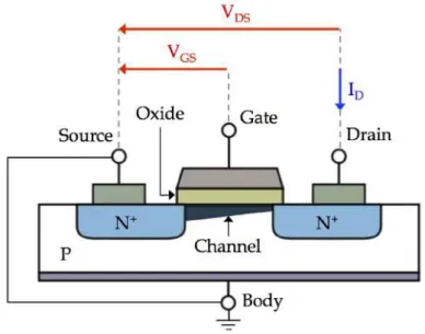
A MOSFET transistor consists in four electrodes, represented in Fig.7: source (S), drain (D), gate (G) and the body (B). It is composed primarily by a large block, the body, of p-type silicon. Into the body, two regions of heavily doped n-type silicon are created to form the source and the drain. Gate is the control-ling terminal and it is isolated from the rest of the transistor by an oxide layer sitting between the gate and the channel. This prevents current from flowing into/out of the gate, resulting in a high input impedances (1012- 1014⌦) and a low power consumption, which make the MOSFET the fastest component during switching operations.
The transistor operation modes are represented in Fig.8aand8b, which de-scribe respectively the ID-VGS and ID-VDS characteristic curves. By applying a potential difference between the gate and the body, the conductive character-istics of the channel region can be changed to allow current flow. If a small positive voltage is applied between gate and body (VGB), the positive potential at the gate repels part of the charges creating a region with a small negative charge known as depletion region. As VGB is increased, the depletion region grows. When VGB is increased beyond some threshold voltage (typically a few V) an inversion layer of electrons is formed near the gate. This provides a conductive channel between drain and source which allows current to flow be-tween source and drain and voltage drop across the two terminals. The body is generally internally connected to the source. This means that the gate to base voltage VGB is the same as the gate to source voltage VGS and to create the inversion layer VGS needs to be above the threshold voltage (Vth). If VGS
is less than Vth, no inversion layer is present and so no current can flow be-tween source and drain and the transistor is said to be cut-off. When VGS is greater or equal to Vth, the transistor is conductive. At this point, if VDS> 0, the positive charge of the drain pulls electron away from the channel to be more distributed around the drain, where the inversion layer is smaller and the de-pletion region is larger than near the source. In this region, where VGS > Vth and VDS < (VGS- Vth), the transistor is in the linear (or ohmic) region. It behaves as a voltage controlled resistor, where VGScontrols the resistance. The current ID does not depend on VDS. As VD is increased, the depletion region near the drain continues to get larger and the inversion layer near the drain continues to shrink. At some point, the inversion layer entirely disappears and the drain is said to be pinched-off. Current still flows between source and drain and the potential difference is so large between the two terminals that electrons are able to push through the pinched-off area that contains few car-riers. However, further increases in VD results in minimal further increases in current, as the additional potential overcome the increased pinched-off region. The transistor is said to be in the saturation region.
Figure 7: General structure of a nMOSFET. Under a positive VGS, the charge carriers flow through the channel between source and drain.
Figure 8: n-type MOSFET characteristics (a) Id= f(VDS) and (b) Id = f(VGS) 2.1.4 IGBT transistor
Insulated Gate Bipolar Transistor (IGBT) is the functional integration of power MOSFET and BJT devices in monolithic form. IGBT was developed in the 1980s by B.W. Scharf and J.D. Plummer to provide a superior alternative to bipolar power transistors [Rus83] [Bal84]. It combines the gate-drive characteristics of MOSFETs (high input impedance and application at high frequency) with the high-current and low-saturation-voltage capability of bipolar transistors (low on state power loss), to achieve the optimal device characteristics. The structure of an IGBT is very similar to a vertical MOSFET (see next section) with the difference that the block connected to the drain terminal is a N+-type substrate in the vertical MOSFET, whereas in an IGBT it is P+-substrate (Fig.9). For this reason the IGBT is often described as an N-channel power MOSFET on top of a p+ type substrate. IGBTs operate in a similar way to MOSFETs. An inversion layer is formed in the P+ area by applying a tension at the gate. However, if the potential of the collector is increased, the flow of electrons draws positive charges from the p-type substrate into the drift region, significantly increasing the conductivity of the channel region and dramatically reducing the voltage of the IGBT. This property gives the IGBTs a higher current density and capability compared to similarly gate-driven MOSFETs, resulting in low on-state power loss. Thus, IGBTs are specially designed to turn on and off rapidly in high-current applications.
2.1.5 Recent solutions: trench technology
In the last years, power semiconductor electronics have rapidly evolved in or-der meet the requirements of new applications involving smaller and smaller
Figure 9: Comparison between (a) a vertical MOSFET and (b) an IGBT. The main dif-ference consists in a n-type substrate in the vertical MOSFET and a p-type substrate in the IGBT (respectively in orange and green).
technology sizes and higher and higher current densities [Bay08] [Ish04a] [Kor09]. The vertical trench technology is the most common configuration that we can find in the market nowadays, for both MOSFETs and IGBTs used in low power and high current densities application. In the following, a brief description of these components is provided, focusing, as example, on a MOSFET device, which is at the base of the technology under investigation in this work.
2.1.5.1 Vertical MOSFET
As suggested by the name, vertical MOSFETs (or VDMOS, Vertical Diffused MOS) differ from the lateral MOSFETs (Fig.7) for their vertical structure (Fig.
10): the source electrode is placed over the drain, resulting in a current mainly vertical when the transistor is in the on-state [Mor96]. More precisely, the source is connected to a highly doped N+ region that is confined insight a P region under the gate. The vertical channel is then formed between the latter and the N- region below, connected to the drain electrode by a N+ layer. The working principle and electrical characteristic curves of a VDMOS are exactly the same of a planar MOSFET (Section 2.1.3):
• If the gate to source voltage (VGS) is lower than a threshold value (Vth), a depletion layer is formed in the P area. The channel is isolated and the transistor is cut-off.
• When VGSis greater than Vth, the carrier inversion layer is formed in the channel and the transistor is in the on state: an electron current, linearly proportional to the tension applied at the gate, flows from the source to the drain.
dimensions, in a vertical structure, the voltage rating of the transistor is a function of the doping and thickness of the N+epitaxial layer, while the current rating is a function of the channel width. This makes it possible for the VDMOS to sustain both high blocking voltage and high current within a compact piece of silicon. For these reasons, vertical power MOSFETs are typically employed in applications that involve high power densities in single device packages of power modules.
Figure 10: Schema of a VDMOS.
2.1.5.2 Trench MOSFET
Different kinds of VDMOS exist depending on their structure: planar MOS, V-groove MOS (VMOS), trench MOS (UMOS), etc.
In a trench MOSFET, also called UMOS, the gate electrode is buried in a trench etched in the silicon. The comparison between a vertical v-groove struc-ture (VMOS) and a trench strucstruc-ture is depicted in Fig.11.
The fabrication process of a trench MOSFET is shortly described by Williams et al. [Wil17]. As shown in Fig.11bafter forming the VDMOS source and body regions, an etched trench of narrow width (e.g., 0.8 to 1.5 µm across) is oxi-dized to form a gate oxide lining the trench and subsequently filled with phos-phorus in situ doped polysilicon. A polysilicon CVD deposition completely fills the trench, overflowing the etched trench onto the silicon surface. Except for a small masked area needed for gate contact, the polysilicon is then "etched back" so that the top surface of the polysilicon gate is recessed, but still overlap-ping the N+source. Subsequent thermal oxidation caps and seals the recessed polysilicon with a protective layer of oxide. A contact mask then selectively exposes the transistor’s surface gate and its numerous cellular source/body regions to an oxide etch (while protecting the oxide above the trench). Af-ter contact etch, metal deposition and photolithographic patAf-terning are per-formed interconnecting a series of separate and distinct trench VDMOS cells into a single three-terminal trench power MOSFET. Except for the polysilicon gate contact, the resulting die surface is nearly planar, so that problematic step coverage issues of the v-groove structure (Fig. 11a) are completely elinated. The resulting cell pitch was half that of any other vertical device, im-proving channel-resistance, epitaxial current uniformity, and total RDS(on). As represented in the graph of Fig. 12, increasing cell density of a trench MOS-FET decreases the devices RDS(on) hyperbolically. In contrast, planar VDMOS or VMOS exhibit a U-shaped dependence, declining in RDS(on) with increasing density before reaching a minimum, then rising rapidly at higher densities as a result of a decrease in channel packing density and poor current uniformity in the epitaxial layer [Wil17].
Figure 11: Cross section of (a) a v-groove VDMOS (or VMOS) and (b) of a trench gate vertical MOSFET (or trench VDMOS) [Wil17].
Figure 12: Impact of cell density on RDS(on). Planar VDMOS exhibits a minimum while trench VDMOS benefits from scaling [Wil17].
2.2 smart power mosfet for the automotive industry: reliabil-ity issue and description of the devices under test
In this work we focus on low voltage MOSFET-based smart power devices used as lightning switches in car and truck applications. Fig. 13a shows an example of e-switch smart power MOSFET from NXP Semiconductors.
Fig. 13b represents the main parts composing the layered structure of a power device for standard low voltage applications:
• Power die. It is theMOSFET active area of the device, consisting mainly in the Si block coated by the source top metallization layer, generally made out of Al or Cu. In the "smart" power modules, the power die is connected to a control die (soldered on the same lead frame) with sensor and protection functionalities.
• Internal bonding connections. They allow a low-resistance current flow through the power die. Al or Cu bonding wires (Fig. 14a) are ones of the most common solution used at the moment. Several wire bondings, which a standard diameter that varies from few tens of micrometers to a maximum of 500µm, are connected in parallel in order to support and distribute high currents. Ribbon (Fig. 14b), clips and ball-bonding (Fig.
14c) are other examples of bonding internal connections that we can find in the commercial power devices.
• Lead frame. It serves primarily to support the chip mechanically during the assembly of plastic packages and to connect the chip electrically with
Figure 13: (a) Power MOSFET device from NXP Semiconductors for low voltage ap-plications. (b) Schematic representation of the cross-section of the power MOSFET. The lead frame, made out of Cu, serves as heat sink and is di-rectly soldered on the PCB. The bonding wires are cold welded on the Al top metallization by ultrasonic process. The device is encapsulated in a plastic mold compound.
Figure 14: Examples of internal bonding connections in a low voltage power module. (a) Cu bonding wires, (b) Al ribbons, (c) ball-bonding [San17].
• Mold compound. It is the most widely used polymer-composite packag-ing material for encapsulatpackag-ing low voltage power devices [Pro03]. The main function of the epoxy-based package is to provide environmental and mechanical protection for the devices. It must deliver a balanced combination of properties in the areas of mechanical strength and tough-ness, chemical resistance, electric insulating performance, thermal con-ductivity and moisture stability in the range of -65 to 200 C. In order to control thermal conductivity, internal stress characteristics and reliability performances, filler particles (commonly made out of silica or alumina) are integrated in the epoxy resin [Ham89].
2.2.1 Stress conditions in power electronics for automotive
Power electronics for automotive must comply with standard qualification re-quirements described in the AEC-Q100 documents, developed by the Auto-motive Electronics Council (AEC) component technical committee. These doc-uments contain detailed qualification requirements for integrated circuit and include failure mechanisms based stress test methods. Components meeting these specifications are suitable for use in the harsh automotive environment.
The basic standard lifetime requirements for passengers vehicles today are: • Lifetime: 15 years
• Operation time: 10.000 hours • Mileage: 300.000 km
In the following, we provide a short description of the main stresses at which power electronics for automotive are subject during their normal operational mode.
2.2.1.1 Thermal stress
During their on-off operating cycles, power components undergo passive and active thermal cycles. They are subject to extremely diverse external climate
conditions. At the same time, when the vehicle is on, the motor compartment warms up to 130 C [Kas01] [Bou08]. This results in passive thermal cycles from - 40 C to 130 C [Sch10]. On the other hand, active thermal cycles correspond to the temperature increase due to Joule heating and thermal dissipation. The combination of these two stresses can severely influence the power electron-ics reliability, especially when the external temperature is high. In automotive applications, power devices are designed to tolerate a maximum operating temperature of 175 . When this value is reached, the integrated control circuit turns the device off as protection. The thermal amplitude in a single on-off cycle is not critical for the materials composing the device layered structure. However, the iteration of these thermal cycles induces important stresses in the electronics components during their life-time due to the difference in the coefficients of thermal expansion (CTE). These stresses can locally induce plas-tic deformation in the softest parts (solders, metallization, bonding wire, mold compounds) and cracks in the most fragile parts (oxides and silicon). This problem of CTE difference will be further addressed in "Source metallization" section (2.2.2.2).
2.2.1.2 Electromagnetic stress
The electromagnetic interferences (due to high tension power lines, mobile phones, radio waves, etc.) and the vehicle system itself can cause a transient electrical noise that can interfere with the electrical components in the vehicle. Ignition and lighting system, electromechanical actuators, starters, alternators, etc. are the source of potential electromagnetic noise. The manufacturer must comply with electromagnetic compatibility and emission regulations [Mar11]. 2.2.1.3 Mechanical and chemical stress
Mechanical stress arises from the deformations and vibrations of the engine system. The parts that are the most sensitive to this stress are the solder joints and the bonding connections.
In addition, the devices are affected by environmental conditions as mois-ture, fog, saline atmosphere, etc. that can cause corrosion in the device com-ponents. The plastic packaging play an important role to protect the power device from the aggressive environmental factors.
2.2.2 Failure modes in power MOSFETs
Reliability is defined as the ability of an item to perform a required function under stated conditions for a certain period of time, which is often measured by probability of failure, by frequency of failure, or in terms of availability
15) as a function of the device life-time. The failure rate in this stage increases with the usage duration and the device aging and this defines the life-time of the device.
Figure 15: Bathtub curve of failure rate.
Considering our specific application field, power switches driving the vehi-cle light system are located far from the engine system. Thus, the mechanical stress and the thermal variations generated by the engine system, can be ne-glected. The main stress they undergone is the electro-thermal one. In fact, during their life, the components undergo several short-circuits and avalanche [Ber10] events, inducing thermo-mechanical effects, added to the normal ther-mal excursions due of the environment in which they operate. These repetitive electro-thermal stresses produce degradation effects at the interfaces between the different materials composing the device structure, because of the differ-ence in their physical properties (table1), and in particular in the coefficients of thermal expansion (CTE).
Fig.16shows a schema of a smart power device with the main critical parts during electro-thermal aging: the solder joint and the metallic parts (source electrode metallization and bonding wires). In the following the associated failure mechanisms are described. In this work, we will focus on the failure mechanisms of the metallic parts.
Table 1: Physical properties of the main representative materials at 25 Cl [Pie11].
Function Semiconductor Conductor Solder
Material Si Al Cu PbSn5Ag2.5
CTE [10-6/K] 4.15 23.1 16.5 21
Young modulus [GPa] 131 70 120 10
Poisson ratio 0.27 0.35 0.34 0.4
El. cond. [⌦-1m-1] (doping dependent) 10-3 37.7 ⇤ 106 59.6 ⇤ 106 6.67 ⇤ 106
Thermal cond. [Wm-1K-1] 148 237 385 50
Thermal capacity [Jkg-1K-1] 752 897 385 150
Figure 16: Schematic representation of a LFET1T-like smart MOSFET power device. The critical points subject to electro-thermal stress are: die/leadframe solder joint, Al source metallization, bonding wires.
Pb-free solders, consisting essentially in Sn-Ag-Cu alloy, are more and more used from the electronics manufacturers. The low elastic limit of these materi-als induces deformation in the solder layer even at low stress. In addition, the CTE mismatch between Si and Cu can strain the solder joint connection, and over the component lifetime can contribute to mechanical solder joint fatigue failure [Lee00]. Two phenomena can then occur during the electro-thermal ag-ing of the device: cavities multiplication and delamination startag-ing from the edges of the solder towards the center (Fig. 17). Both of them limit the cur-rent flow in the solder layer, increasing the RDS(on) of the device. It has been demonstrated that the less is the solder thickness the more fragile is the solder [Hay02] [You15] [Gué02]. However, an increase in the thickness results in a in-crease in the thermal resistance of the solder layer, because of the low thermal conductivity of the materials constituting the solder. A trade-off between ther-mal conductivity and mechanical strength is then required in phase of design of the solder interface.
Figure 17: Delamination of a lead-free solder joint between the die Si substrate and the Cu lead frame [Bou08].
2.2.2.2 Failure modes in the active zone
The active zone of the power device corresponds to the MOSFET die and the bonding wires connected to the source metallization. In this area, the electro-thermal cycles induce mechanical stress in the softest parts of the complex layered structure that, by nature, consists in the interconnection of different ma-terials (metal-oxide-semiconductor) and constitutes the MOSFET device. They are the Al source metallization and bonding wires, which have higher coeffi-cient of thermal expansion respect to the oxide and the Si (table1).
Source metallization
Reconstruction of the aluminum metallization is an effect observed since the early times of microelectronics [San69] [Phi71]. During thermal cycling of IGBT and MOSFET devices, periodical compressive and tensile stresses are intro-duced in the thin metalization film by the different CTEs of the aluminum and of the silicon chip, due to the large thermo-mechanical mismatch between both materials and due to the stiffness of the silicon substrate [Cia02]. The thermo-mechanical stresses in the Al results in the gradual change in its granular structure. Fig.18 shows the comparison between the Al metallization surface in a power MOSFET before and after electro-thermal cycles. The aged metal is characterized by an higher roughness and cracks along the grain boundaries.
Figure 18: Electro-thermal ageing of the source electrode metallization in a smart power MOSFET. Scanning electron micrograph of the (a) fresh metalliza-tion and (b) at failure [Pie11].
To assess the stress seen in interconnects during operation, Flinn and cowork-ers [Fli87] considered the simplest approximation of a chip: a metal layer de-posited on a silicon substrate. They measured the stress arising during thermal
needed, along with the substrate Young’s modulus and Poisson’s ratio (Esand ⌫). The film stress f is then directly deduced from the radius of curvature R measured by the laser. Because the substrate is more rigid and does not plastically deform at room temperature, most of the plasticity is expected to occur in the metallic film. In their first paper, the metallization was an Al-1%Si thin film and the cycles were performed from room temperature to 400 C at a rate of about 20 C/min. During the process, the Al layer would go from slightly tensile to compressive stresses (max 100 MPa) during heating, before deforming plastically in tension during the cooling, up to a stress of 300 MPa (Fig. 19).
Figure 19: (a) Typical stress-temperature cycle for a 1-µm-thick poly-crystalline Al film on oxidized Si substrate (Tmax ⇠ 450 C ). (b) Finite element simulation showing the Von Mises stresses generated by a temperature change of 50 C in a 1 cm x 2cm x 0.5 mm specimen (typical size used in wafer curvature) [Leg09].
Several publications followed (a nice and recent review can be found in Wiederhirn’s thesis [Wie07] and established that the film strength 1 increased as the inverse of the film thickness. This increase in film thickness was then ra-tionalized in term of threading dislocation movements by Nix in 1989 [Nix98], 1 During thermal cycles, metallic thin films experience two yield stresses, at the end of the elastic compression stage (heating) and in tension during cooling. The maximum stress is usually reached at the end of the cooling and is considered as the "film’s strength"- see [Leg06]
from an initial calculation of image forces in thin films by Matthews and Blakeslee [Mat74] [Mat75]. Later on, this model was questioned [Mue98] [Leg09] because the amorphous layer between the Si substrate and the metal film (usu-ally Si oxide), acted as a dislocation sink. This later effect may however reflect an artifact of TEM observation because Si oxide seems to soften significantly under electron beam [Zhe10]. In any case, the reversible motion of threading dislocations (Nix’s model) cannot explain the strong and non-crystallographic roughening of Al films on Si, observed in power mosfets ([Pie11] or plain thin Al films on substrates [Tur92] [Leg05] [Kao03].
Another approach consisted in applying the Frost and Ashby deformation mechanisms maps [Fro82] to the stress/temperature cycles. These maps and equation were established for bulk materials and link a given plastic strain rate ˙✏ to a given stress and temperature. By comparing the predicted stress/temper-ature cycles using these maps and the experimentally established one (by laser curvature), Bostrom [Bos01] showed that a large discrepancy existed between both approaches, underlying the fact that thin films on substrate deformed in a specific way.
Recently, a qualitative model adapted to the bamboo-microstructure of thin film was developed to explain how the plastic deformation proceeded by atomic self diffusion of Al atoms along the grain boundaries (GBs) [Mar14]. These GBs, acting as fast diffusion paths would gradually open during tension (cool-ing phase). Dur(cool-ing heat(cool-ing, the Al atoms are expelled to the surface through the same GBs, as predicted by the model from Gao [Gao99], and contribute to its roughening. The irreversibility of the process is due to the native oxidation of cracks surfaces that will prevent crack healing during compression.
Bonding wires
Reliability of bonding connections in power modules, and in particular of wire bonds soldered on the source electrode metallization by cold-bonding process, is an important issue for the reliability of power systems because of extending operation temperatures (due to the Joule effect in the wire itself and to the power dissipation in the Si substrate) which induce high levels of thermo-mechanical stress in the bonding area [Cia02] [Gla04] [Dup07]. Ramminger et al. [Ram00] described and modeled this cyclic stress as wire flexure by thermal expansion or wire deformation under mechanical shock loading if the bond surfaces are able to move relatively to each other (Fig.20).
As consequence of this stress, mainly two kinds of failures of wire bonds have been reported in the literature:
1. Heel crack failure (Fig.21a), originating from bending caused by thermal expansion or by mechanical deformation of the wire [Meh99] [Cia02].
Figure 20: Bonding wire subjected to cyclic mechanical stress applied by lateral dis-placement of one bonding area relatively to the other in Ramminger et al. experiments [Ram00].
2. Bond wire lift-off (Fig. 21b), resulting from material fatigue at the chip metallization. This is caused by shear forces which result from the differ-ent coefficidiffer-ents of thermal expansion on the interface [Ber98] [Cia02]. These degradation modes have been mainly observed in components that un-dergo active cycles and rarely under extreme conditions (avalanche or short-circuit). In the latter case, the metallization is the location most prone to degra-dation, but even in the cases of faster bonding failure, metallization reconstruc-tion is always observed [Sme11].
The failure mechanisms at the bonding connections are generally studied combining experimental test and simulation. Ramminger has demonstrated, by a finite element model based on stress experiments, that the number of cy-cles to heel crack failure is strongly dependent on the loop geometry [Ram00]. He has also considered that cracks in the bonding wires and at the wire-metallization interface do not propagate towards the wire-metallization because of its higher yield strength [Ram98]. The layout of the bonding connection also play a role in the reliability of power device. According to Ishiko et al., the re-liability of IGBT components can be improved by optimizing the wire position configuration by thermo-electric simulation in order to make the temperature distribution of the devices more uniform [Ish06].
In parallel to the studies in simulation, the microstructure of the bonding wires has been inspected in order to investigate the influence of the grain structure evolution on the crack growth and the device life-time. Yamada et al. [Yam07] showed that the crack growth increases with the number of ther-mal cycles (from -40 C to 200 C), resulting in a reduction of the residual bonding length of Al wires that seems to be independent by the limited re-crystallization of the wire grains at high temperature.
Figure 21: Examples of bond failures in power components: (a) heel crack failure [Cia02] and (b) wire lift-off [Den17].
2.2.3 Thermosensitive aging indicators
The electro-thermal aging of power devices, either IGBTs or MOSFETs, is as-sociated with the evolution of the electrical parameters, such as VT H, IDSsat, on-state resistance (RDS(on)). They are then aging indicators as they can be mon-itored during the device testing procedures to assess its aging and predict their life-time. During our characterization we have focused on the RDS(on)evolution. 2.2.3.1 RDS(on)
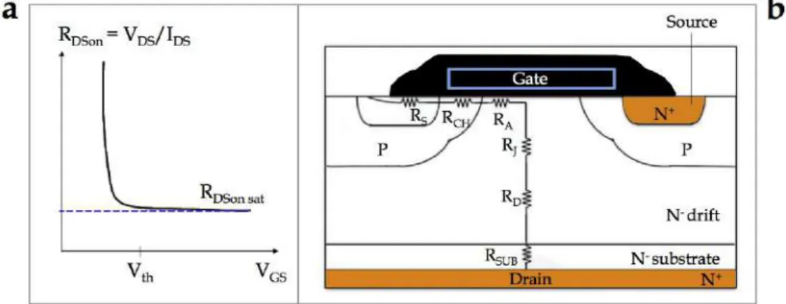
During the on state, in the linear region, the VDMOS can be considered as a re-sistance between drain and source: the RDS(on), defined as the ratio between the drain voltage and current when VDSapproaches zero (Fig.22a). It is one of the main parameters of a power MOSFET: the goal during the design of a power MOSFET is to lower this resistance in order to limit the device self-heating and the voltage reduction during the on state. The RDS(on) value depends on the voltage applied at the gate terminal, and so on the channel size.
The on-state resistance RDS(on) can be considered as the sum of several com-ponents as shown in Fig.22b:
RDS(on)(VGS) = RS+ RCH(VGS) + RA(VGS) + RJ+ RD+ RSUB (2) Where:
• RS = Source diffusion resistance.
It is made up of three elements: the bonding wires resistance (Rwire), the metallization layer resistance (Rmetal) and the N+ wells resistance (RN+).
It represents one of the main contribution to the total RDS(on) and it is inversely proportional to the channel width and, for a given die size, to the channel density:
RCH = W 1
LeffC0µE(VG)(VGS- Vth)
(3) where W and Leffare respectively width and length of the channel, C0the electrical capacitance of the gate oxide per surface unit, µE the electron mobility in the inversion layer and Vththe threshold voltage. On the basis of this equation, three solutions can be adopted to lower the RDS(on):
1. Shortening the inversion channel length (Leff). However after a limit value (pinch-off) we have the formation of a gap between the source and the drain [Mor96].
2. Increasing VGS. However, for voltage higher than 20 V there is the risk to damage the gate oxide.
3. Increasing the inversion channel length (W) per surface unit by de-creasing the single cell sizes.
• RA = Accumulation resistance.
It represents the resistance of the accumulation region in the epitaxial zone under the gate electrode, where the direction of the current changes from horizontal (in the channel) to vertical (to the drain contact). The resistance is described by the following equation [Sun80]:
RA= 1 3 1 W L0effC0µa(VG)(VG- VTD) (4) whereµa is the electron mobility in the accumulation layer, L0eff the ef-fective length of the channel in depletion mode and VDT a voltage de-pending on the doping concentration inside the epitaxial region. In order to reduce this resistance, the channel length needs to be increased, that means that the power device cells must be tightened.
• RJ= "JFET" component-resistance between two P body regions.
It is due to the formation of a bottleneck in the charge carrier path be-tween the two P areas. This is the detrimental effect of the cell size reduc-tion menreduc-tioned above: the P implantareduc-tions form the gates of a parasitic JFET transistor that tend to reduce the width of the current flows in the N-epitaxial region. This junction is modulated by VDS: an increase in VDS determines the bottleneck shrinkage. In order to prevent this contribution increasing the RDS(on), the distance between the transistor cells must be increased, contrary to the considerations made for the other resistances. • RD= Drift region resistance
It represents the resistance of the epitaxial layer. The role of this layer is to sustain the blocking voltage, so RDis directly related to the voltage rating of the device. A high voltage MOSFET requires a thick, low-doped and highly resistive epitaxial layer, whereas a low-voltage transistor requires a thin layer with a higher doping and less resistive layer. As a result, RDis the main factor responsible for the resistance of high-voltage MOSFETs. • RSUB= Substrate resistance
It is the resistance of the drain, including the resistance of the N+ sub-strate (RN+) and the package connection. The RN+ contribution here is significantly higher than in the source because of the higher thickness of the drain layer (few hundreds microns). However, RSUB is overall lower than RSbecause of the absence of the wire bondings (the device substrate is directly soldered on the Cu lead frame).
In power MOSFET-based devices for low voltage and high current applica-tions, like the components studied in this work, the sum of the source and drain contributions (RS+RSUB) represents more or less the 50% of the total RDS(on). In this study, we focus on the metallization that shows degradation and thus resistance increase during electrical cycling [Kho07b].
2.2.4 Devices under test: 45V and 65V LFET1T technology
LFET1T is the commercial name of the technology developed in 2008 by NXP Semiconductors (at that time Freescale) for automotive low voltage (< 48V) and frequencies (< 1 kHz) applications and based on trench MOSFET modules. Two versions of this technology have been characterized in this work:
1. 12V SPD06 (Fig.23a), designed for 12 V batteries in car applications, with breakdown voltage of 45V. They consists in 2 MOSFET sectors, each one connected by 3 bonding wires and having a RDS(on) of 6 m⌦.
Figure 22: MOSFET vertical structure, showing the total resistances that make up RDSon.
2. 24V T07D17 (Fig. 23b), designed for 24V batteries in truck applications, with breakdown voltage of 65V. They consists in 5 MOSFET sectors, con-nected by 8 bonding wire and having a RDS(on)of 17 m⌦ and 7 m⌦. The trench MOSFET structure, with a small cell pitch of ⇠ 1 - 2µm (Fig. 24b) allows the LFET1T modules to get three times higher channel current densities (> 1000mA/in2) compared to the previous generation of NXP power MOSFET devices based on a planar structure (Fig. 24a), together with a reduction in die and package sizes (and thus cost). However, this also implies a higher possibility of thermal instability of the device. For this reason, an isolated poly-diode for temperature sense has been integrated in the technology. The details of the technology are summarized in table 2, showing a comparison between the 12V SPD06 and 24V T07D17 modules. The composition and thickness of the source metallization and bonding wire are the same in both modules. The source metallization consists in an aluminum (Al) film of 0.5 wt% of copper (Cu) and tungsten (W), coated (only in the 24 V devices) by a 0.5µm thick SiO2 passivation layer everywhere, except in the bonding areas. The wire bonds are made out of pure Al and have a diameter of 400µm. The Al bonding wires are contacted to the Al source metallization by a classical cold-bonding process by ultrasound [Bro15] [Goe12]. The bonding parameters are reported in table
3. The bonding force of 10 N applied to an area of 450 ⇤ 750µm2 results in a bond stress of ⇠ 30MPa. These values are in line with the bonding parameters optimized by Goehre [Goe12].
Table 2: LFET1T Technology Differences. LFET1T 45V LFET1T 65V SPD06 T07D17 4.0µm 5.3µm Epi 0.50⌦ ⇤ cm 0.85⌦ ⇤ cm P-edge Implant B11, 120keV B11, 110keV P-deep Implant B11, 200keV B11, 220keV
ISD Poly 6K, As 6K, As
Single wafer Single wafer Al (Cu, W) Al (Cu, W) Source metal 3.6µm 3.6µm / SiO2 Metal passivation 0.5µm Al Al Bonding wire 400µm 400µm
Table 3: Bonding parameters.
Bonding force 10 N
Bonding pressure 37 MPa
Bond width 450 µm
Bond length 750 µm
Bond Area 0.265 mm2 (elliptical)
Figure 23: LFET1T smart power MOSFET device from NXP Semiconductors. (a) 45V, 12V SPD06, (b) 65V, 24V T07D17.
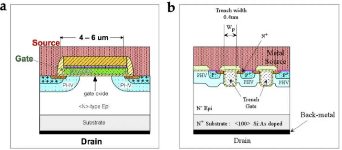
Figure 24: (a) planar vs (b) trench MOSFET structure in NXP power devices. 2.3 reliability assessment of lfet1t power devices:
methodol-ogy and accelerated aging test description.
The reliability assessment of power devices is a complex issue that can be ad-dress following different approaches. Fig. 25 shows a methodology schema representing the three approaches that are currently adopted to study the ro-bustness of power electronics systems:
1. Experimental testing. The reliability assessment is addressed experimen-tally by:
• Accelerating aging test to reproduce the stress at which the device is subject.
• Localization and identification of the failure. • Degradation analysis of the critical points.
2. Degradation mechanisms modelling. The goal is to determine: • Accelerating aging factors.
• Life-time predictive laws. • New design strategies. 3. Numerical study, to simulate:
• The stresses undergone by the device.
• The correlation between the stresses and the degradation mecha-nisms.
On the basis of the mission profile, these three methods (or a combination of them) contribute to provide a predictive evaluation of the device life-time and to identify the degradation physical mechanisms.
Figure 25: Methodology used to assess the reliability of power devices. In this work we use an experimental approach to assess the degradation of the metallic parts of LFET1T power devices under repetitive accelerated aging conditions. This work is based on the first approach and tries to give a contribution in the investigation of the degradation mechanisms of the critical points in power devices undergone accelerated electro-thermal aging test. In particular here we focus on the degradation of the metallic parts of of LFET1T power dies. The degradation of the Al source metallization, together with the wire bondings, (section2.2.2) is assessed following a physical metallurgy approach, described in detail in the next chapter, in order to understand the degradation mechanisms behind the failure of LFET1Ts. The qualification tests used by the microelectronics community, together with the failure localization techniques (SAM, x-rays, OBIRCH, etc.) are nowadays well standardized (AECQ100 stan-dard for the automotive). However, the physical mechanisms at the base of the failure are still difficult to comprehend, because of rapid technology evolution, and of the lack of standard quantification methods. Here we try to offer some paths to quantify the degradation occurring in the source metal through the development of new investigation technologies and systematic measurements of the structure and microstructure of the Al metallization and wires. These dedicated techniques and quantification methods could serve as references for the investigation of other devices.
In this work, the aging tests have been performed in intermittent operating life (IOL) mode, which consists in applying cyclical electrical pulses until the device failure (Fig.26). This choice is motivated by previous studies [Kho07a]
Figure 26: IOL (Intermittent Operating Life) test: the device undergoes electrical pulses during the time interval ton. The test current and ton values are generally limited by the control die, that protects the control die from "bulb inrush" phenomena.
LFET1T devices have undergone two different kinds of IOL accelerated electro-thermal test:
1. Tests at NXP on 65V LFET1T (T07D17).
They consist in qualification tests, used by the manufacturers to deter-mine the device life-time, in conformity with the AECQ100-12 standard [Kel06]. The objective is to reproduce the power device behaviour in their normal operating mode, regulated by the control die. A repetitive short-circuit (SC) is imposed to the power die. At this point the control die detects a current overflow and turns the power die off. Energy is dissi-pated at this stage, leading to an increase in the device temperature and affecting the device aging conditions.
2. Tests at Satie laboratory on 45V LFET1T (SPD06).
These tests are complementary to the previous ones: they have been de-signed in order to push the devices to their technology limits and moni-tor the electrical aging indicamoni-tors during the tests. For these tests, SPD06 devices have been assembled without control die and mold compound, and put under extreme SC conditions in a test bench designed by the Satie laboratory [Ros13]. This original configuration gave us the possibil-ity to bypass the current regulation of the control die and to control the dissipated energy by playing on the duration of the SC pulses (tON).
During both tests, only one sector undergoes the electrical pulses, the one inside the red rectangle in 45V LFET1Ts (Fig.27a) and 65V LFET1Ts (Fig.27b), so we could use the others as reference during the microstructural characteri-zations.
The test features and conditions are summarized in Table5 and detailed in the next two sections.
Figure 27: Localization of the MOSFET sector under accelerated aging test (red rect-angle) in a (a) LFET1T 45V (SPD06) and (b) LFET1T 65V (T07D17) power device.
![Table 1: Physical properties of the main representative materials at 25 Cl [ Pie11 ].](https://thumb-eu.123doks.com/thumbv2/123doknet/2151434.9267/35.892.162.825.260.475/table-physical-properties-main-representative-materials-cl-pie.webp)
![Figure 17: Delamination of a lead-free solder joint between the die Si substrate and the Cu lead frame [ Bou08 ].](https://thumb-eu.123doks.com/thumbv2/123doknet/2151434.9267/36.892.229.664.655.883/figure-delamination-lead-free-solder-joint-substrate-frame.webp)