Vapor Phase Doping with N-type Dopant into Silicon by Atmospheric Pressure Chemical Vapor Deposition
Shotaro Takeuchi, Ngoc Duy Nguyen, Frederik Leys, Roger Loo, Thierry Conard, Wilfried Vandervorst and Matty Caymax
IMEC, Kapeldreef 75, B-3001 Leuven, Belgium
Atomic layer doping of phosphorus (P) and arsenic (As) into Si was performed using the vapor phase doping (VPD) technique. For increasing deposition time and precursor gas flow rate, the P and As doses tend to saturate at about 0.8 and 1.0 monolayer of Si, respectively. Therefore, these processes are self-limited in both cases. When a Si cap layer is grown on the P-covered Si(001), high P concentration of 3.7 × 1020 cm-3 at the heterointerface in the Si-cap/P/Si-substrate layer stacks is achieved. Due to As desorption and segregation toward the Si surface during the temperature ramp up and during the Si-cap growth, the As concentration at the heterointerface in the Si-cap/As/Si-substrate layer stacks was lower compared to the P case. These results allowed us to evaluate the feasibility of the VPD process to fabricate precisely controlled doping profiles.
Introduction
Atomically-controlled processing and delta doping technology are required for advanced Si electronic devices such as heterojunction bipolar transistors and complementary metal-oxide-semiconductor field effect transistors (MOSFETs) with ultra shallow junctions (USJs). So far, low energy ion implantation has been widely used in order to fabricate shallow source/drain regions. However, there are several issues such as implantation damages and channeling effect related to this method. Additionally, the fabrication of USJs for the source/drain regions with conformal doping in three-dimensional FETs such as FinFETs leads to additional challenges coming from the shadowing effect by the ion implantation. Therefore, atomic layer deposition (ALD) techniques such as atomic layer epitaxy (ALE) and vapor phase doping (VPD) as alternative techniques are currently being considered in the CMOS process flow [1,2]. In these ALD approaches, the dopant atoms are deposited on the Si surface through the thermal decomposition of gaseous precursors such as diborane (B2H6), phosphine (PH3) and arsine (AsH3) in a standard chemical vapor deposition (CVD) reactor or gas source molecular beam epitaxy system. Subsequently, they are diffused into the substrate by a drive-in anneal [3] or by epitaxial incorporation under one or more successive monolayers (MLs) of epitaxial Si for the dopant activation. Because the deposition follows the device topography [1,2], these ALD techniques are expected to lead in a natural way to fully conformal junctions, precisely controlled doping process and sharp doping profile without any damages.
It is known that the VPD process with phosphorus (P) as n-type dopant on Si or SiGe surface shows a self-limited reaction, but not VPD with boron (B), at given conditions [4~6]. On the other hand, the behavior of arsenic (As) has to be clarified. Because the diffusion coefficient of As in Si is lower than that of P [7], it will be useful to fabricate
USJs with As for the source/drain regions in MOSFETs. Therefore, in the present work, we performed VPD with P and As at various growth conditions by atmospheric pressure CVD and we studied the amount of as-deposited dopant atoms as function of doping parameters. In this work, the doped structures did not receive any additional thermal anneal.
Experimental Details
The VPD process was performed on blanket 200 mm Si(001) wafers in a standard horizontal cold wall, load-locked, ASM EpsilonTM 2000 reactor. After loading into the reactor, the wafer received a bake at high temperature of 1050oC to remove the native oxide. Then a 50 nm-thick Si buffer layer was grown at 650oC using SiH4 at reduced pressure. Subsequently, the wafer was cooled down to the dopant gas exposure temperature in H2 ambient. The VPD was performed at 400~600oC at atmospheric pressure by using PH3 and AsH3 0.1% diluted in H2. The PH3 or AsH3 flow was 50 ~ 200 standard cubic centimeters per minutes (sccm) during 0.1~100 minutes. Hydrogen or nitrogen was used as a carrier gas during the VPD step. After the VPD step, a Si cap was eventually deposited on the dopant-covered Si at 650oC in H2 ambient or at 575oC in N2 ambient using SiH4 at reduced total pressure. SiH4 partial pressure for the Si cap ranges from 70 to 79 Pa. The total dose and concentration were determined respectively by angle-resolved X-ray photoemission spectroscopy (XPS) for P or As/Si-substrate structures and secondary ion mass spectroscopy (SIMS) for Si-cap/P or As/Si-substrate structures.
Results and Discussion
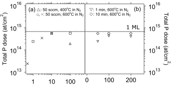
The dependence of the P and As dose, as measured by XPS, on the dopant flow and the exposure time in P and As/Si structures are shown in Figs. 1 and 2. In the case of VPD with PH3 50 sccm and H2 as carrier gas at 400oC, no P atom on the Si surface could be detected by XPS, even with an exposure time of 100 min. When N2 is used as carrier gas at 400oC with PH3 50 sccm, P atoms could neither be detected by XPS after 1, 3 or 10 min of exposure to PH3. However, after 100 min, the P dose on the Si surface was estimated to be 1.9 × 1014 cm-2 which is equal to 0.3 monolayer (ML), where 1.0 ML is defined by the total surface site density of 6.8 × 1014 cm-2 on Si(001), as shown in Fig. 1(a). In the case of VPD temperature of 600oC and PH3 flow of 50 sccm in N2 as carrier gas, the P dose tends to immediately saturate at about 0.8 ML when the exposure time is increased. We have confirmed the reproducibility of this value in two batches as shown in Fig. 1(a). The process is thus self-limited under the chosen conditions. As shown in Fig. 1(b), when the PH3 flow is increased at 600oC for fixed exposure time, the amount of P atoms adsorbed on the Si surface is increased and saturates at about 0.8 ML at a certain exposure time.
The variations in the P dose can be explained as follows. In the case of VPD at 400oC with H2 as carrier gas, because the Si surface cools down to 400oC in H2 after the growth of the Si buffer layer at 650oC and because H2 is used as carrier gas during the VPD step, the Si surface is passivated by hydrogen. It was reported that PH3 dissociatively adsorbs on the Si surface and consumes four available surface sites for the adsorption of one P atom and three H atoms below 400oC [8]. Additionally, it was also reported that H desorption from the Si surface starts at 400 ~ 450oC [9,10]. Therefore, there is no available site for the PH3 molecules to dissociatively adsorb at 400°C, which means that
PH3 adsorption is suppressed due to the passivation of the Si surface by hydrogen. For VPD at 400oC with N2 as carrier gas, the amount of available sites for the PH3 adsorption on the Si surface increases relatively compared to the case of H2 as carrier gas. However, the P dose on the Si surface is very low because there are not sufficient available sites for the PH3 adsorption. In contrast, for VPD at 600oC with N2 as carrier gas, many adsorption sites for PH3 are available because most of the H atoms are desorbed from the Si surface above 580oC [10]. As a result, the P dose of about 0.8 ML can be achieved, as shown in Fig. 1.
So far, systematic studies about the self-limited behavior of P on Si(001) at various conditions have been reported by Murota group [4,5,11]. The P dose tends to saturate at 2.0 ~ 3.0 ML for exposure temperature between 450oC and 750oC and low pressure conditions using a PH3/He gas mixture. In their case, the PH3 partial pressure was 0.26 ~ 0.35 Pa at low total pressure. In contrast, our PH3 partial pressure is in the range 0.34 ~ 1.33 Pa under atmospheric total pressure. Although the PH3 partial pressure in this work is higher than in their case, the P dose in Refs. [4,5,11] is about 2 ~ 3 times higher than in our case. These results strongly suggest that the amount of P dose is influenced by the partial pressure of H2.
In the case of VPD with AsH3 in N2 as carrier gas at 600oC with an exposure time ranging from 0.1 ~ 100 min, although As atoms could not be detected by XPS after 0.1 min of exposure to AsH3, the As dose also tends to saturate at about 1.0 ML with increasing exposure time and flow rate of AsH3, as shown in Figs. 2(a) and 2(b). In this case, the process is also self-limited under the chosen conditions. In both cases, atomic layer doping for n-type dopant on the Si surface has been achieved by the VPD technique.
10
1310
1410
1510
16T
o
tal P dose (at
/cm
2)
200
100
0
PH
3flow rate (sccm)
10
1310
1410
1510
16To
ta
l P do
se (a
t/cm
2)
1
10
100
PH
3exposure time (min)
(a)
(b)
Figure 1. Total P dose in P/Si-substrate structures as function of (a) the PH3 exposure time with fixed PH3 flow of 50 sccm and (b) PH3 flow rate at 600oC as measured by angle resolved-XPS with take-off angles between 20o to 80o. Each symbol indicates the VPD process conditions, Ƒ for 1st batch and × for 2nd batch: VPD at 600oC, U: VPD at 400oC in Fig. 1(a) and V: VPD for 1 min, : VPD for 10 min in Fig. 1(b). The dotted line shows the level of 1 ML Si.
1 ML
U: 50 sccm, 400oC in N2
Ƒ, ×: 50 sccm, 600oC in N2
V: 1 min, 600oC in N2
Figure 2. Total As dose in As/Si-substrate structures as function of (a) the AsH3 exposure time with fixed AsH3 flow of 50 sccm and (b) AsH3 flow rate for 1 min as measured by angle resolved-XPS with take-off angles between 20o to 80o. The VPD process was performed at 600oC under atmospheric pressure. The dotted line shows the level of 1 ML Si.
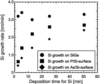
In the VPD technique, as mentioned above, one possible way to activate the dopants is to epitaxially incorporate them under successive MLs of Si. Therefore, we have investigated the Si growth rate (GR) [nm/min] on P- or As-covered Si and the behavior of P and As atoms during the Si-cap/P/Si-substrate or Si-cap/As/Si-substrate layer stacks growth. Figure 3 shows the Si GR on P- or As-covered Si-surface as function of the SiH4 deposition time after the VPD step using a 10 min PH3 or AsH3 flow of 50 sccm. As mentioned above, the Si surface is covered by a 0.8 ML P or 1.0 ML As atoms respectively after the VPD step. As reference, a Si layer was grown on SiGe buffer at 575oC and reduced pressure using N2 as carrier gas. We obtained 3.2 nm/min for the pure Si GR on SiGe by spectroscopic ellipsometry measurements [12]. When the deposition starts on the P- or As-covered Si-surface, the Si GR is significantly reduced during the initial growth stage. It was reported that during in-situ doping processes, the surface potential of the P- or As-covered Si could be more negative than that of pure Si surface because P and As have a lone pair of electrons relative to Si [13]. In contrast, SiH4 has partially ionic Si+-H- bonds. This indicates that incident SiH4 molecules are repelled by the P- or As-covered Si surface with negative surface potential, resulting in a depression of the Si GR. When the deposition time for the Si-cap growth is increased, the Si GR on P- or As-covered Si surface approaches the pure Si GR. This is because the P or As surface concentration decreases and the negative surface potential generated by P or As atoms on the Si surface simultaneously decreases as the Si-cap growth occurs. However, it should be noticed that the Si GR on P- or As-covered Si-surface never reaches the pure Si GR in this deposition time range. This result might be related to a memory effect: auto-doping from residual P or As inside the reactor or high surface concentration of P or As at the growing surface due to the effect of dopant segregation [14,15]. Additionally,
1 ML
10
1310
1410
1510
16Tot
al
As dos
e (
a
t/c
m
2)
200
100
0
AsH3 flow rate (sccm)
10
1310
1410
1510
16Tot
al
As dose (
a
t/
c
m
2)
1
10
100
AsH3 exposure time (min)
(a)
50 sccm, 600oC in N2 1 min, 600(b)
othere is a difference in the Si GR between P-covered Si and As-covered Si, which will be discussed here below.
Figure 3. Si growth rate on SiGe and n-type dopant covered Si-surface. The different symbols relate to the growth of Si on different surfaces; Ɣ: Si growth on SiGe, Ŷ: Si growth on P/Si-surface, and ¡: Si growth on As/Si-surface.
Figure 4(a) shows the P concentration profile of the Si-cap/P/Si-substrate layer stacks grown with different parameters, as obtained by SIMS. The Si surface is exposed here to a PH3 flow of 50 sccm during 10 min. The Si-cap which is grown from SiH4 has a typical thickness of about 50 nm. The expected P concentration peaks are observed in the SIMS measurement for each of the studied conditions. We observed an increase of the dopant concentration when the PH3 exposure temperature was increased, while the P concentration decreased by increasing the Si cap growth temperature. The total P dose, as estimated from SIMS measurements (Fig. 4(b)), is lower when the Si-cap is present compared to the initial P dose obtained from the XPS data. It is well known that the deposited n-type dopant such as P and As on the Si surface starts to desorb between 550oC to 600oC of substrate temperature [16,17]. 1017 1018 1019 1020 1021 Tot al P conc ent ra ti on ( a t/ cm 3 ) 100 80 60 40 20 0 Depth (nm) 1019 1020 1021 1022 1023 Si c onc ent ra tion ( a t/cm 3 ) Si(650°C)/P(600°C)/Si Si(650°C)/P(400°C)/Si Si(575°C)/P(600°C)/Si Si(575°C)/P(400°C)/Si Si reference 1 ML 1012 1013 1014 1015 T o ta l P dose (a t/ c m 2 ) cS i( 5 7 5 °C ) /P (4 00 °C ) cS i( 5 7 5 °C ) /P (6 00 °C ) cS i( 6 5 0 °C ) /P (4 00 °C ) cS i( 6 5 0 °C ) /P (6 00 °C ) (a) (b)
Deposition time for Si [min]
Si g row th ra te [nm /m in] 0 1.0 2.0 3.0 4.0 0 10 20 30 40 50 60 Si growth on SiGe Si growth on P/Si-surface Si growth on As/Si-surface
Deposition time for Si [min]
Si g row th ra te [nm /m in] 0 1.0 2.0 3.0 4.0 0 10 20 30 40 50 60 Si growth on SiGe Si growth on P/Si-surface Si growth on As/Si-surface 0 1.0 2.0 3.0 4.0 0 10 20 30 40 50 60 Si growth on SiGe Si growth on P/Si-surface Si growth on As/Si-surface Si growth on SiGe Si growth on P/Si-surface Si growth on As/Si-surface
Figure 4. (a) SIMS profiles and (b) total dose of as-deposited P on Si at 400oC or 600oC capped by a Si film grown at 575oC or 650oC. The Si-cap is denoted by cSi. The solid line shows the level of 1 ML of Si in Fig. 4(b).
Actually, in the case of the Si-cap(575oC)/P(600oC)/Si-substrate layer stack, the total P dose is reduced from 5.5 × 1014 cm-2 for the initial P dose on the Si surface, as measured by XPS, to 2.6 × 1014 cm-2 for the P dose in the Si-cap/P/Si-substrate layer stack by SIMS. In the case of the Si-cap(650oC)/P(600oC)/Si-substrate layer stack, the total P dose is estimated to be 4.6 × 1013 cm-2 by SIMS, which is one order of magnitude lower than the initial P dose. Obviously, P desorption occurred during the ramping up to the Si-cap growth temperature after the PH3 exposure. However, high P concentration of 3.7 × 1020 cm-3 at the heterointerface in the Si-cap(575oC)/P(600oC)/Si-substrate layer stack was achieved even after the Si-cap growth. Additionally, it was observed that P atoms segregate toward the Si surface during the Si-cap growth. The P concentration near the Si surface is between 1.0 × 1019 cm-3 to 2.0 × 1019 cm-3, which explains why the Si GR on P-covered Si does not reach the pure Si GR.
Figure 5(a) shows the SIMS result for the As concentration profiles of the cap/As/substrate layer stacks grown under similar growth conditions as for the cap/P/substrate case. Concerning the dopant concentration, similar trends as for the Si-cap/P/Si-substrate structures were observed. In contrast, the As distribution shows a completely different behavior, compared to the Si-cap/P/Si-substrate case. The As peak could only be observed in the Si-cap(575oC)/As(600oC)/Si-substrate layer stack. Additionally, the As atoms strongly segregate toward the Si surface during the Si-cap growth. The As concentration near the Si surface is estimated to be 3.0 × 1019 cm-3. This is also the reason why the Si GR on As-covered Si does not reach the pure Si GR. Figure 5(b) shows the total As dose in the Si-cap/As/Si-substrate layer stacks as estimated from SIMS measurements. In the case of the Si-cap(575oC)/As(600oC)/Si-substrate layer stack, the total As dose is reduced from 6.8 × 1014 cm-2 before the Si-cap growth to 1.0 × 1014 cm-2 after the Si-cap growth. Compared to the P case, As atoms easily desorb during the temperature ramp up for the Si-cap growth.
Figure 5. (a) SIMS profiles and (b) total dose of as-deposited As on Si at 400oC or 600oC capped by a Si film grown at 575oC or 650oC. The Si-cap is denoted by cSi. The solid line shows the level of 1 ML of Si in Fig. 5(b).
1017 1018 1019 1020 1021 T o ta l A s c o n c e n tr a ti o n (a t/c m 3 ) 100 80 60 40 20 0 Depth (nm) 1019 1020 1021 1022 1023 Si c once nt ra tio n ( a t/cm 3 ) Si(650°C)/As(600°C)/Si Si(650°C)/As(400°C)/Si Si(575°C)/As(600°C)/Si Si(575°C)/As(400°C)/Si Si reference 1 ML 1012 1013 1014 1015 To ta l A s d o s e (a t/c m 2 ) c S i( 575 °C ) /A s (400 °C ) cSi( 5 7 5 °C ) /A s (600° C ) c S i( 650 °C ) /A s (400 °C ) cSi( 6 5 0 °C ) /A s (600° C ) (a) (b)
Desorption and segregation during the ramping up of the substrate temperature and the Si-cap growth after the VPD step are found to be another emerging problems for n-type doping into Si. However, these problems can be solved by choosing appropriate growth conditions and introducing more reactive Si precursor gas at low temperature such as trisilane (Si3H8) [18]. Because the deposition temperature for Si-cap layer can be reduced by using Si3H8, it would result in the suppression of the dopant desorption and segregation during the ramping up of the substrate temperature and the Si-cap growth. As an alternative way for the fabrication of FinFETs with conformal USJs, a thin SiO2 layer grown at low temperature instead of the Si-cap would be also useful to protect the As or P atomic layer from desorption during the drive-in anneal for the dopant activation [3].
Conclusion
We have performed n-type doping of Si with P and As by using the VPD technique. In both cases, we have confirmed atomic P and As layer doping with self-limiting behavior on the Si surface by XPS, which means that an atomic layer of n-type dopant has been achieved on Si by the VPD technique. At this moment, our results clearly show that the strong point of the VPD approach is the control of the amount of n-type dopant on the Si substrate without any damage in the structure. For the n-type atomic layer doping with Si-cap layer, a high P concentration of 3.7 × 1020 cm-3 at the heterointerface in the Si-cap/P/Si-substrate layer stack was achieved. In the case of Si-cap/As/Si-substrate layer stacks, we have observed a strong segregation effect during the Si-cap growth compared to the P case. Because of the desorption of P and As at already around 550oC ~ 600oC, a thin cap layer of Si or SiO2 grown at low temperature will be needed prior to the drive-in anneal.
Acknowledgments
Fruitful discussion with Dr. Lijun Yang (IMEC) is gratefully acknowledged. Ilse Hoflijk (IMEC) is also gratefully acknowledged for XPS measurement.
References
1. C. Rochefort, R. van Dalen, N. Duhayon, and W. Vanderworst, in Proceedings ISPSD, pp. 237–240 (2002).
2. N. D. Nguyen, F. Leys, S. Takeuchi, R. Loo, M. Caymax, P. Eyben, and W. Vandervorst, presented at ISTDM 2008, Abstract book pp. 229.
3. K. W. Koh, H. J. Oh, H. Choi, H. Kurino, and M. Koyanagi, Mat. Sci. Eng. B 89, 435 (2002).
4. Y. Shimamune, M. Sakuraba, T. Matsuura, and J. Murota, Appl. Surf. Sci.
162-163, 390 (2000).
5. Y. Chiba, M. Sakuraba, and J. Murota, Semicond. Sci. Technol. 22, S118 (2007). 6. B. Tillack, Thin solid films, 318, 1 (1998).
7. S. M. Sze, Physics of Semiconductor Devices 2nd edition, J. Wily and Sons, (1981).
8. M. L. Yu, D. J. Vitkavage, and B. S. Meyerson, J. Appl. Phys. 59, 4032 (1986). 9. P. Gupta, V. L. Colvin, and S. M. George, Phys Rev. 37, 8234 (1988).
10. S. M. Gates, Surf. Sci. 195, 307 (1988).
12. The growth rate on the primary SiGe surface is slightly higher than the growth rate on Si, because Ge-H bond is weaker than Si-H bond. However, when a few atomic layers of Si are deposited, the initial growth rate decreases and reaches a stationary value.
13. C.-A. Chang: J. Electrochem. Soc. 123, 1245 (1976).
14. X. Liu, Q. Tang, T. I. Kamins, and J. S. Harris, J. Crystal Growth 251, 651 (2003). 15. M. Yang, M. Carroll, J. C. Sturm, and T. Büyüklimanli, J. Electrochem. Soc. 147,
3541 (2000).
16. L. Kipp, R. D. Bringans, D. K. Biegelsen, J. E. Northrup, A. Garcia, and L. -E. Swartz, Phys. Rev. B 52, 5843 (1995).
17. L. Kipp, R. D. Bringans, D. K. Biegelsen, and L. -E. Swartz, Phys. Rev. B 50, 5448 (1994).
18. F. Leys, R. Bonzom, B. Kaczer, T. Janssens, W. Vandervorst, B. De. Jaeger, J. Van Steenbergen, K. Martens, D. Hellin, J. Rip, G. Dilliway, A. Delabie, P. Zimmerman, M. Houssa, A. Theuwis, R. Loo, M. Meuris, M. Caymax, and M. M. Heyns, Mat. Sci. Semicond. Proc. 9, 679 (2006).