UNIVERSITÉ DE MONTRÉAL
MODE COMPOSITE WAVEGUIDE FOR 5G AND FUTURE WIRELESS COMMUNICATION SYSTEMS
JIAPIN GUO
DÉPARTEMENT DE GÉNIE ÉLECTRIQUE ÉCOLE POLYTECHNIQUE DE MONTRÉAL
THÈSE PRÉSENTÉE EN VUE DE L’OBTENTION DU DIPLÔME DE PHILOSOPHIAE DOCTOR
(GÉNIE ÉLECTRIQUE) JUIN 2018
UNIVERSITÉ DE MONTRÉAL
ÉCOLE POLYTECHNIQUE DE MONTRÉAL
Cette thèse intitulée :
MODE COMPOSITE WAVEGUIDE FOR 5G AND FUTURE WIRELESS COMMUNICATION SYSTEMS
présentée par : GUO Jiapin
en vue de l’obtention du diplôme de : Philosophiae Doctor a été dûment acceptée par le jury d’examen constitué de :
M. NERGUIZIAN Chahé, Ph. D., président
M. WU Ke, Ph. D., membre et directeur de recherche M. AKYEL Cevdet, Ph. D., membre
DEDICATION
To my wife Shiyu Cai To my daughter Anna Xinyan Guo To my parents and my brother
ACKNOWLEDGEMENTS
I would like to thank my PhD research director, Prof. Ke Wu for giving me this opportunity to pursue my PhD study at Ecole Polytechnique de Montreal in Canada. His guidance helped me to understand and think of solutions for the challenges in the 5G and future wireless communication. I would like to thank the technical personnel Mr. Jules Gauthier, Mr. Traian Antonescu, Mr. Steve Dube and Mr. Maxime Thibault in Poly-Grames Research Centre for the help in fabrication and measurement of the prototypes.
I would like to thank Mr. Jean-Sébastien Décarie for the assistance of software problems, also Mrs. Rachel Lortie and Mrs. Nathalie Lévesque for the administrative procedures of the department.
I would like to thank Dr. Tarek Djerafi, Dr. Fang Zhu and Dr. Jianfeng Gu for the valuable discussions and helpful suggestions during my struggles in the PhD study, and Dr. Pascal Burasa for helping me with the French translation of the abstract.
I would like to thank my friends Kuangda Wang, Yangping Zhao, Lianfeng zou, Shabnam Ladan, Jaber Moghaddasi, Ajay Babu Guntupalli, Yifan Yin, Wencui Zhu, Xiaoqiang Gu, Desong Wang, etc., who made my stay at Ecole Polytechnique de Montreal memorable.
I would like to thank my father Jian Guo and mother Bin Xu, who taught me a lot and supported my decision at every stage of my life and encouraged me to pursue PhD degree in Canada.
Last but most importantly, my heart-felt gratitude goes to my wife Shiyu Cai and my daughter Anna Xinyan Guo, who have accompanied me through my PhD study. I would like to thank my wife for her enduring love and support during the highs and lows of the past several years. Without her encouragements all along, I may not achieve what I have today.
RÉSUMÉ
Dans les systèmes de communication sans fil modernes, les fonctionnalités haut-débit et multi-bande des circuits RF et micro-ondes sont de plus en plus requises dans des systèmes intégrés et compacts. La bande de fréquence actuellement utilisée pour les communications sans fil commerciales comprend les bandes aux alentours de 900 MHz, 1,9 GHz, 2,45 GHz, 3,5 GHz et 5,8 GHz pour la téléphonie mobile, l'Internet sans fil et la connectivité des capteurs. Les nouvelles bandes millimétriques comme la bande de fréquence V (57-66 GHz) et la bande E (71-76 GHz et 81-86 GHz) sont utilisées pour la connectivité des microcellules et du cœur du réseau.
Le nouveau standard des communications sans fils 5G nécessite l’exploitation parallèle de bandes de fréquences, à savoir les basses et les hautes fréquences, permettant ainsi d’aller au-delà de la capacité des systèmes de communications actuels. D’une part, la demande croissante pour un meilleur débit de données nécessite une bande de fréquence beaucoup plus large, ce qui justifie le recours vers la bande de fréquences millimétriques. D'autre part, le standard LTE ainsi que les autres systèmes de communication à grande couverture doivent être développés de manière compatible avec les bandes de fréquences en bas de 6 GHz et celles qui sont au-delà de 6 GHz. Par conséquent, la mise au point de nouveaux systèmes intégrés et à bas coût capables d’opérer sur fréquences UHF et millimétriques s’avère essentielle pour le standard sans fil émergent (5G). Dans cette thèse, une nouvelle méthode de conception de circuits intégrés RF large bande et multi-bande, appelée guide d'ondes à modes composites (MCW), est proposée et étudiée. Le MCW est constitué d’une structure à double guide d'ondes interne et externe, où la structure externe agit comme une ligne coaxiale rectangulaire adaptée pour les basses fréquences, tandis que la structure interne fonctionne comme un guide d'onde rectangulaire pour les hautes fréquences, ce qui rend la structure plus simple, plus compacte et à faibles pertes d’insertion. Le MCW est susceptible de propager des signaux au sein du guide d'ondes interne suivant le mode TE10 et/ou au sein du guide d'onde externe avec le mode TEM en fonction de la fréquence, permettant ainsi d’aboutir à des performances optimales pour les deux bandes de fréquences (basse et haute). Pour ce faire, les paramètres fondamentaux du guide d'ondes et les modes d'ordre supérieur du MCW sont théoriquement étudiés. Des équations pour les constantes de propagation, les impédances, les pertes et les fréquences de coupure du mode supérieur des guides d'ondes interne et externe du MCW sont calculés.
Les prototypes MCW sont fabriqués au sein de notre centre de recherches Poly-Grames en utilisant la technique des circuits intégrés multicouches (3 couches). Les règles de conception MCW, commençant par le choix du substrat (la permittivité et l'épaisseur), le calcul des dimensions ainsi que les bandes de fréquences d’opération, sont étudiés en détail. Cependant, ce concept MCW n'est pas limité seulement à la technique du guide d’onde intégré au substrat (GIS), mais il peut également être mis en œuvre en utilisant d'autres technologies telles que LTCC, CMOS et l'impression 3D. Deux types de réseaux d'alimentation (à savoir le type I et le type II) sont d'abord conçus pour les mesures et l'intégration du MCW avec d'autres circuits planaires. Dans les deux cas, les réseaux d’alimentation MCW multicouches sont transférés sur des lignes micro-rubans standards, ce qui est pratique pour les mesures.
En utilisant ces réseaux d'alimentation, divers circuits multicouches basés sur le MCW sont développés grâce à l'exploitation de ses différentes propriétés. Un coupleur directionnel MCW à 10 GHz est développé, où la conversion des modes en relation avec le couplage de puissance du guide d'ondes interne et externe est étudiée. Le principe de fonctionnement du coupleur est théoriquement analysé pour obtenir les équations régissant le comportement des ondes aux différents ports du coupleur.
Un filtre MCW bi-mode à 10 GHz utilisant le guide d'ondes interne comme alimentation d’entrée-sortie, et le guide d'onde externe comme résonateur, est également développé. Les deux modes dégénérés dans le résonateur à guide d'ondes externe sont utilisés pour le fonctionnement du filtre bi-mode, ce qui aboutit à deux pôles de transmission et un zéro de transmission finie. Un T magique planaire est également développé à 10 GHz en se basant sur la technique MCW, utilisant le guide d'ondes interne comme port de sommation et le guide d'onde externe comme port de soustraction du T magique. Le signal du guide d'onde externe est divisé équitablement mais en opposition de phase entre les deux ports de sortie, tandis que le signal du guide d'onde interne est couplé avec la même phase aux deux ports de sortie.
Grâce à la géométrie et la symétrie des modes du MCW, un guide d'onde composite demi-mode (HMCW) est également proposé et étudié. Comme le MCW, le HMCW dispose également d'un guide d'ondes interne et externe, dont chacun fonctionne en demi-mode. Dans la structure HMCW, le signal se propage dans le guide d'ondes interne avec le mode quasi-TE0.5-0 et tout au long du guide d'onde externe avec le mode quasi-TEM. Comparé au MCW, le HMCW n'occupe que la
moitié de l'espace requis, en ayant une performance comparable en termes de perte d’insertion. Un réseau d'alimentation pour le HMCW est également développé dans le but de simplifier les mesures et l'intégration, où les deux guides d'ondes (interne et externe) sont transférés à des lignes micro-ruban à une seule couche.
ABSTRACT
In modern wireless communication systems, broadband and multiband functionalities of RF and microwave circuits are often required in a highly integrated and geometrically compact front-end systems. The currently used frequency band for commercial wireless communication includes the lower bands of 900 MHz, 1.9 GHz, 2.45 GHz, 3.5 GHz and 5.8 GHz for mobile phone, wireless internet and sensor connectivity, as well as the emerging millimeter-wave (mmW) bands of V-band (57-66 GHz) and E-band (71-76 GHz and 81-86 GHz) for small cell and backhaul connectivity. The emerging 5G wireless communication system requires the deployment of both low- and high-dual frequency bands in a simultaneous manner, which should extend far beyond the capability of existing mobile communication systems. On one hand, the increasing demand for higher speed wireless data transmission requires a much larger bandwidth, where the mmW bands shall be exploited to accommodate such a bandwidth increase. On the other hand, the LTE and other long-ranged wireless platforms need to be developed in a backwards-compatible way, and it is also very important to accommodate the frequency bands below 6 GHz or sub-6-GHz frequency ranges. Therefore, the development of a low-cost and integrated hardware solution is essential for the 5G and future wireless communication systems, which should be able to support the emerging wireless deployments over an unprecedented wide UHF-to-mmW frequency range.
In this thesis, the development of a broadband or multi-band hardware design platform or building technology, called mode composite waveguide (MCW), is proposed and addressed. The MCW consists of inner and outer wave-guiding duo structures, where the outer structure acts as a rectangular coaxial line suitable for lower frequency operation for its compact size, while the inner structure works as a rectangular waveguide suitable for higher frequency operation thanks to its simple structure and low loss. The MCW can propagate signals in the inner waveguide with TE10 mode and/or the outer waveguide with TEM mode depending on frequency to achieve optimal performance for both low and high frequency operations.
To begin with, the fundamental waveguide parameters and higher order modes of MCW are theoretically analyzed. Equations for propagation constants, impedances, losses, and higher order mode cutoff frequencies of both the inner and outer waveguides of MCW are provided respectively. The MCW prototypes are fabricated on three layers of substrates using the multilayer substrate integration techniques in our Poly-Grames Research Center. The MCW design rules, from the
substrate selection such as permittivity and thickness to the choice of MCW dimensions and operation frequency bands, are discussed in detail. However, this MCW concept is not only limited to the substrate integration technique, and other technologies such as LTCC, RF CMOS and 3D printing can also be used for implementation.
Two types of joint feeding networks (namely type I and type II) are first developed for MCW measurement and integration with other planar circuits. In both cases, the multilayer MCWs are transitioned to single layer microstrip lines, which are convenient for measurements. Using these joint feeding networks, various multilayer circuits based on the MCW are developed through the exploitation of its different properties. A MCW directional coupler at 10 GHz is developed, where the mode conversion regarding the inner and outer waveguide power coupling is studied. The operation principle of the coupler is mathematically formulated in achieving the required power summation and cancellation. A MCW based dual-mode filter at 10 GHz is developed, which uses the inner waveguide as the input and output feedings, and the outer waveguide as the dual-mode resonator. The two degenerate modes in the outer waveguide resonator are used for the dual-mode filter operation, which generates two transmission poles and one finite transmission zero. A MCW based planar magic tee at 10 GHz is also developed, which uses the inner waveguide as the summation port and the outer waveguide as the difference port for the magic tee operation. The outer waveguide signal is equally divided and goes into the two output ports out of phase, while the inner waveguide signal is coupled to the two output ports in phase through the two slots on the middle layer.
Taking advantages of the geometrical and mode symmetry of MCW, a half-mode composite waveguide (HMCW) is also proposed and studied. Like the MCW, the HMCW also has an inner and outer waveguide, each working in its half-mode operation, respectively. In the HMCW structure, the signal propagates in the inner waveguide with quasi-TE0.5-0 mode and in the outer waveguide with quasi-TEM mode. Compared to its full-size counterpart, the HMCW only occupies half the space, while exhibits a comparable transmission loss performance. A joint feeding network for the HMCW is also developed for measurement and integration, where both the inner and outer waveguides are transitioned to single layer microstrip lines.
TABLE OF CONTENTS
DEDICATION ... III ACKNOWLEDGEMENTS ... IV RÉSUMÉ ... V ABSTRACT ... VIII LIST OF TABLES ... XIII LIST OF FIGURES ... XIV LIST OF SYMBOLS AND ABBREVIATIONS ... XX
CHAPTER 1 INTRODUCTION ... 1
1.1 Background and Motivation ... 1
1.1.1 Rectangular Waveguide and Substrate Integrated Waveguide ... 1
1.1.2 Coaxial Line and Substrate Integrated Coaxial Line ... 2
1.1.3 Mode Composite Waveguide ... 3
1.2 Outline of thesis ... 5
CHAPTER 2 THEORETICAL ANALYSIS AND FABRICATION PROCESS ... 7
2.1 Theoretical Analysis of Mode Composite Waveguide ... 7
2.1.1 Outer Waveguide Parameters ... 7
2.1.2 Inner Waveguide Parameters ... 10
2.2 Parametric Study of Mode Composite Waveguide ... 11
2.2.1 Impedance Parametric Study ... 11
2.2.2 Loss Parametric Study ... 13
2.3 Higher Order Mode Analysis ... 16
2.3.1 Higher Order Mode Cutoff Frequency ... 17
2.4 Fabrication of Mode Composite Waveguide ... 21
2.5 Dimension of Mode Composite Waveguide ... 23
2.6 Conclusion ... 24
CHAPTER 3 JOINT FEEDING NETWORK OF MODE COMPOSITE WAVEGUIDE ... 25
3.1 Outer Waveguide Feeding Network ... 25
3.2 Inner Waveguide Feeding Network ... 28
3.3 Type I MCW Joint Feeding Network ... 30
3.3.1 Feeding Network Design ... 30
3.3.3 Fabrication and Measurement ... 32
3.4 Type II MCW Joint Feeding Network ... 36
3.4.1 Feeding Network Design ... 36
3.4.2 Fabrication and Measurement ... 39
3.5 Conclusion ... 43
CHAPTER 4 MODE COMPOSITE WAVEGUIDE CIRCUITS ... 44
4.1 MCW Directional Coupler ... 45
4.1.1 Coupler Operation Principle ... 46
4.1.2 Coupler Analysis and Design ... 47
4.1.3 Fabrication and Measurement ... 52
4.2 MCW Dual-Mode Filter ... 54
4.2.1 Dual-Mode Filter Design ... 55
4.2.2 Fabrication and Measurement ... 61
4.4 MCW Magic Tee ... 63
4.4.1 Magic Tee Analysis and Design ... 64
4.5 Conclusion ... 70
CHAPTER 5 HALF-MODE COMPOSITE WAVEGUIDE ... 72
5.1 HMCW Theoretical Analysis ... 72
5.2 HMCW Parametric Study ... 74
5.3 Joint Feeding Network Design ... 82
5.4 Fabrication and Measurement ... 86
5.5 Conclusion ... 90
CHAPTER 6 MULTILAYER CIRCUIT AND ANTENNA ... 91
6.1 Variable Propagation Constant Directional Coupler ... 91
6.1.1 Coupler Operation Principle ... 91
6.1.2 Coupler Analysis and Design ... 93
6.1.3 Fabrication and Measurement ... 96
6.2 Balanced Antipodal Linear Tapered Slot Antenna ... 99
6.2.1 Balanced ALTSA Design ... 100
6.2.2 Integrated Feeding Network Design ... 103
6.2.3 Fabrication and Measurement ... 106
6.3 Conclusion ... 108
CHAPTER 7 CONCLUSION AND FUTURE WORK ... 110
7.1 Conclusion ... 110
7.2 Future Work ... 112
REFERENCES ... 114
LIST OF TABLES
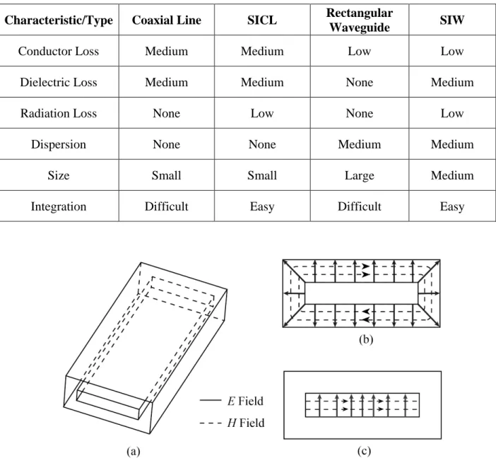
Table 1.1: Comparison of different types of waveguides and transmission lines. ... 4
Table 2.1: Comparison of outer waveguide higher order mode cutoff frequencies. ... 19
Table 4.1: Design parameters of MCW forward and backward directional couplers. ... 48
Table 4.2: Dimensions of type I and type II dual-mode filters. ... 58
Table 5.1: Comparison of HMCW, waveguides and transmission lines. ... 74
Table 6.1: Forward and backward directional coupler design parameters. ... 95
Table 6.2: Dimensions of balanced ALTSA. ... 102
LIST OF FIGURES
Figure 1.1: 3D illustration of SIW. ... 2 Figure 1.2: 3D illustration of SICL. ... 3 Figure 1.3: (a) 3D illustration of MCW, the E and H field distributions of its two fundamental
modes: (b) TEM mode in outer waveguide, (c) TE10 mode in inner waveguide. ... 4 Figure 2.1: Outer and inner waveguides of MCW and their fundamental modes: (a) TEM mode in
outer waveguide, (b) TE10 mode in inner waveguide. ... 7 Figure 2.2: Unit length capacitance distribution in a thin rectangular coaxial line. ... 9 Figure 2.3: Dimensions of the inner and outer waveguides of MCW. ... 11 Figure 2.4: Simulated impedance of the inner and outer waveguides at different width and
permittivity (Zin inner waveguide impedance and Zout outer waveguide impedance). ... 12 Figure 2.5: Simulated impedance of the inner and outer waveguides at different height and
permittivity (inner waveguide impedance Zin and outer waveguide impedance Zout). ... 13 Figure 2.6: Calculated dielectric and conductor losses of inner and outer waveguides of MCW at
different widths (RT/duroid 6002, εr=2.94, h=0.508 mm at 50 GHz). ... 14 Figure 2.7: Calculated dielectric and conductor losses of both inner and outer waveguides at
different frequencies (RT/duroid 6002, εr=2.94, h=0.508 mm, w=2.54 mm). ... 15 Figure 2.8: Fundamental and higher order modes E field distributions of outer waveguide (a)
fundamental mode, (b) folded TE20 I, (c) folded TE20 II, (d) folded TE40 I, (e) folded TE40 II. ... 16 Figure 2.9: Simulated dispersion diagram of outer waveguide, including the fundamental TEM
mode and first four higher order modes (RT/duroid 6002, εr=2.94, w=2.54 mm, h=0.508 mm). ... 17 Figure 2.10: Outer waveguide cross section and its equivalent circuit for TRM. ... 18 Figure 2.11: Calculated monomode regions for the inner and outer waveguides at different width. ... 21 Figure 2.12: Fabrication process of the substrate integrated MCW ... 22
Figure 2.13: 3D view and dimensions of substrate integrated MCW. ... 23
Figure 3.1: 3D view, dimensions of microstrip line to outer waveguide transition in back-to-back setup, and the E field distributions and impedances at each denoted position. ... 26
Figure 3.2: Pictures of the front side (a) and back side (b) of the fabricated MCW with microstrip to outer waveguide transition. ... 27
Figure 3.3: Simulated and measured S-parameters of the back-to-back microstrip line to outer waveguide transition. ... 27
Figure 3.4: 3D view and dimensions of the microstrip line to inner waveguide transition. ... 28
Figure 3.5: Pictures of the front side (a) and back side (b) of the fabricated microstrip to inner waveguide transition. ... 29
Figure 3.6: Simulated and measured S-parameters of the back-to-back microstrip line to inner waveguide transition. ... 29
Figure 3.7: 3D view and dimensions of type I MCW joint feeding network. ... 31
Figure 3.8: Pictures of the front side (a) and back side (b) of the fabricated MCW. ... 32
Figure 3.9: MCW four-port back-to-back measurement setup ... 33
Figure 3.10: Simulated E field distribution at 9 GHz (top), and simulated and measured S-parameters of the type I MCW joint feeding network for low frequency operation (bottom). ... 34
Figure 3.11: Simulated E field distribution at 33 GHz (top), and simulated and measured S-parameters of the type I MCW joint feeding network for high frequency operation (bottom). ... 35
Figure 3.12: 3D view and dimensions of the type II joint feeding network. ... 37
Figure 3.13: Fundamental modes of the inner (a) and outer (b) waveguides, and the first two higher order modes of the outer waveguide (c) and (d). ... 38
Figure 3.15: Simulated E field distribution at 9 GHz (top), and simulated and measured S-parameters of the type II MCW joint feeding network for low frequency operation (bottom). ... 41 Figure 3.16: Simulated E field distribution at 19 GHz (top), and simulated and measured S-parameters of the type II MCW joint feeding network for high frequency operation (bottom). ... 42 Figure 4.1: Two fundamental propagating modes in the MCW: (a) TE10 mode in inner waveguide
and (b) TEM mode in outer waveguide. ... 44 Figure 4.2: Dispersion diagram of the outer and inner waveguides of MCW. ... 45 Figure 4.3: Diagram of a general two-hole directional coupler. ... 46 Figure 4.4: Dimensions of MCW backward directional coupler and its joint feeding network. ... 50 Figure 4.5: Simulated coupling power levels at different diameters of the circular slot at 10 GHz. ... 51 Figure 4.6: Simulated feeding network transmission loss of the outer waveguide’s fundamental and
higher order modes. ... 51 Figure 4.7: Pictures of fabricated MCW backward directional coupler: (a) top view, (b) bottom
view. ... 52 Figure 4.8: Comparison of measured and simulated MCW backward directional coupler return loss
(S11) and insertion loss (S21). ... 53 Figure 4.9: Comparison of measured and simulated MCW backward directional coupler isolation
(S31) and coupling (S41). ... 54 Figure 4.10: Fundamental modes of the inner (a) and outer (b) waveguides, and the first two higher
order modes of the outer waveguide (c) and (d). ... 55 Figure 4.11: Simulated E-field distributions of the folded TE202 I mode (a) and folded TE202 II
mode (b) in the dual-mode resonator. ... 56 Figure 4.12: 3D view and dimensions of MCW based dual-mode filter and its corresponding
Figure 4.13: Simulated S21 of type I filter, exhibiting its left transmission zero location at different slot offset. ... 59 Figure 4.14: Simulated S21 of type II filter, exhibiting its right transmission zero location at
different slot offset. ... 60 Figure 4.15: Simulated S-parameters of type I and type II dual-mode filters. ... 61 Figure 4.16: Pictures of the fabricated type I dual-mode filter: front side view (a) and back side
view (b). ... 62 Figure 4.17: Simulated and measured S-parameters of fabricated type I dual-mode filter. ... 62 Figure 4.18: E-field transformation of outer ((a)->(c)->(e)) and inner ((b)->(d)->(f)) waveguides at
magic tee junction. ... 63 Figure 4.19: 3D view and dimensions of the MCW magic tee. ... 65 Figure 4.20: Pictures of the front side (a) and back side (b) of the fabricated MCW magic tee. .. 68 Figure 4.21: Simulated and measured S-parameters at the difference port P1 of the magic tee. ... 69 Figure 4.22: Simulated and measured S-parameters at the summation port P2 of the magic tee. .. 69 Figure 5.1: Cross section view and basic mode profile of HMCW and MCW structures with modes
propagating in the inner and outer waveguides: (a) quasi-TEM mode, (b) TEM mode, (c) quasi-TE0.5,0 mode, (d) TE10 mode. ... 73 Figure 5.2: Dimensions of the HMCW inner and outer waveguides, where the distance between
the inner and outer conductors is kept the same. ... 75 Figure 5.3: Comparison of calculated and simulated fringe effect of the outer waveguide at different
width to height ratio. ... 77 Figure 5.4: Comparison of calculated and simulated fringe effect of the outer waveguide at different
relative permittivity. ... 78 Figure 5.5: Comparison of simulated HMCW and MCW inner and outer waveguide impedances
versus normalized width. ... 78 Figure 5.6: Comparison of simulated HMCW and MCW inner and outer waveguide losses as a
Figure 5.7: Field distribution of the 1st higher order mode of the HMCW outer waveguide and comparison of simulated outer waveguide dispersion diagram of the HMCW and the MCW. ... 80 Figure 5.8: Field distribution of the 1st higher order mode of the HMCW inner waveguide and
comparison of simulated inner waveguide dispersion diagram of the HMCW and the MCW. ... 81 Figure 5.9:3D, cross-sectional and top views of the HMCW joint feeding network. ... 83 Figure 5.10: Mode transformation of a two-stage dual taper structure of the HMCW outer
waveguide feeding network with E field distribution at each denoted position. ... 84 Figure 5.11: Mode transformation of a super compact right angle bend of the HMCW inner
waveguide feeding network with E field distribution. ... 85 Figure 5.12: Pictures of fabricated HMCW joint feeding network front side (a) and back side (b). ... 87 Figure 5.13: E field distribution in the outer waveguide at 9 GHz, and simulated and measured S-parameters of the back-to-back HMCW joint feeding network for low frequency operation. ... 88 Figure 5.14: E field distribution in the inner waveguide at 25 GHz, and simulated and measured S-parameters of the back-to-back HMCW joint feeding network for high frequency operation. ... 89 Figure 6.1: 3D view and dimensions of the proposed directional coupler (a) 3D view, (b) top view,
(c) bottom view. ... 94 Figure 6.2: Pictures of fabricated forward and backward directional couplers: (a-b) top and bottom
view of forward directional coupler, (c-d) top and bottom view of backward directional coupler. ... 96 Figure 6.3: Measured and simulated forward directional coupler: (a) return loss (S11) and insertion
loss (S21), (b) isolation (S31) and coupling (S41). ... 97 Figure 6.4: Measured and simulated backward directional coupler: (a) return loss (S11) and
Figure 6.5: E-field distribution at the cross section: (a) conventional ALTSA, (b) balanced ALTSA.
... 101
Figure 6.6: Top and 3D view of the proposed balanced ALTSA. ... 101
Figure 6.7: Simulated radiation patterns and cross-polarizations of conventional and balanced ALTSA at 28 GHz. ... 102
Figure 6.8: Top and 3D view of the proposed transition for antenna feeding. ... 104
Figure 6.9: Simulated S-parameters and phase difference of the proposed transition. ... 105
Figure 6.10: Top (a) and bottom (b) view of the fabricated balanced ALTSA. ... 106
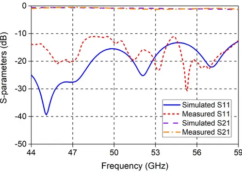
Figure 6.11: Measured and simulated antenna return losses. ... 107
LIST OF SYMBOLS AND ABBREVIATIONS
ALTSA Antipodal Linearly Tapered Slot Antenna CPW Coplanar Waveguide
HMCW Half-Mode Composite Waveguide MCW Mode Composite Waveguide MIMO Multiple-Input and Multiple-Output mmW millimeter-wave
PCB Printed Circuit Board
RF Radio Frequency
SIW Substrate Integrated Waveguide SICL Substrate Integrated Coaxial Line TRM Transverse Resonance Method TE Transverse Electric
TEM Transverse Electromagnetic UHF Ultra High Frequency
VPC Variable Propagation Constant 5G Fifth Generation
CHAPTER 1
INTRODUCTION
1.1 Background and Motivation
Modern development in wireless communication systems requires highly integrated and geometrically compact radio frequency (RF) and microwave circuits and modules featuring broadband and multiband functionalities. The most widely used frequency bands for commercial wireless communications such as mobile phone and wireless internet connectivity are allocated in the low microwave frequency ranges up to 6.0 GHz, covering popular or legacy bands of 900 MHz, 1.9 GHz, 2.45 GHz, 3.5 GHz and 5.8 GHz [1].
To enable agile and ubiquitous connectivity for a wide range of heterogeneous data transmission scenarios including environment- or user-defined smart radio platforms and for internet of things (IoT) with the integration of variable wireless functionalities, the emerging fifth generation (5G) wireless techniques should extend far beyond the capability of existing and current mobile communication systems. One of the 5G speculated technologies is to deploy both low and high frequency bands in a simultaneous manner. Within the 5G platform, some of the key enabling technologies include massive MIMO, carrier aggregation, low-latency technique, device-to-device link, and mmW cellular architecture. On one hand, the demand for high speed (> 10 Gbit/s) data transmission requires a larger bandwidth. To accommodate such a bandwidth increase, the carrier frequency over the mmW range is being considered for small cell and backhaul connectivity such as V-band (57-66 GHz) and E-band (71-76 GHz and 81-86 GHz) [2]. On the other hand, LTE and other long-ranged wireless platforms continue to evolve in a backwards-compatible way and will be an important part of the 5G wireless ecosystem for frequency bands below 6 GHz. Therefore, it is imperative to create low-cost and integrated hardware solutions, which should be able to support emerging wireless deployments over an unprecedented wide UHF-to-mmW frequency range. To this end, the development of a broadband or multi-band design platform is addressed in this thesis.
1.1.1 Rectangular Waveguide and Substrate Integrated Waveguide
The rectangular waveguide is widely used in the design and development of high frequency circuits and systems thanks to its simple structure, low loss, high quality factor, and high-power handling capability. Also as a fully-shielded structure, the interference between neighboring
waveguide circuits can be ignored completely. However, as a single-conductor structure, the rectangular waveguide presents a geometry-dependent cut-off frequency for its fundamental propagation TE10 mode, which limits its use at low frequencies. Furthermore, the integration of such a three-dimensional rectangular waveguide with planar circuits is an important challenge.
To mitigate the underlying problems of integration, a substrate integrated rectangular waveguide was proposed and demonstrated in [3]. The resulting planar topology provides a very promising solution for the development of microwave and mmW circuits and antennas, and today it has been widely known as Substrate Integrated Waveguide (SIW). The SIW consists of two rows of metallized vias embedded in a dielectric substrate that connects the top and bottom metal plates, thereby forming the side walls (shown in Figure 1.1). Due to its similarity with reference to rectangular waveguide, the SIW has a fundamental TE10 propagation mode. The SIW inherits the above-mentioned advantages of rectangular waveguide while fully realized in planar form and easily integrated with other planar circuits. A wide range of low-cost and high-performance SIW circuits and antennas have been developed [3], [4], [5] and [6].
Figure 1.1: 3D illustration of SIW.
1.1.2 Coaxial Line and Substrate Integrated Coaxial Line
On the other hand, the coaxial line is a well-established popular type of non-dispersive TEM mode transmission line with zero cut-off frequency, which makes it suitable for low frequency operation. Unlike the rectangular waveguide having a geometrical dimension related to its cut-off frequency, the dimension of coaxial line can be designed to be small in support of low-to-high frequency operations. The coaxial line is also a fully-shielded structure, which is desirable for
minimizing interference in a high-density circuit. However, the coaxial line is difficult to integrate with planar circuits because of its fully enclosed inner conductor. Besides the integration, as frequency goes higher into mmW, the loss of coaxial line increases significantly, and a high fabrication precision of the inner and outer conductors is also required.
To overcome the integration issue of coaxial line with planar circuits, a substrate integrated form of coaxial line was proposed in [7], called Substrate Integrated Coaxial Line (SICL). The SICL consists of a printed rectangular coaxial structure, laterally shielded by metallized via arrays (shown in Figure 1.2). Like coaxial line, the SICL has a fundamental TEM propagation mode. The SICL also inherits most of the advantages of coaxial line. The SICL is fabricated in a planar form and can be easily integrated with other passive and active circuits and antennas. Numerous SICL-based components and techniques have been demonstrated with different processing techniques [7], [8], [9], [10], [11], [12] and [13].
Figure 1.2: 3D illustration of SICL.
1.1.3 Mode Composite Waveguide
As discussed in the previous section, the advantages and disadvantages of coaxial line, rectangular waveguide and their substrate integrated counterparts are summarized in Table 1.1.
To make use of the advantages of both rectangular waveguide and rectangular coaxial line in support of simultaneous low and high frequency design and development, a new transmission line called Mode Composite Waveguide (MCW) is proposed in this thesis as shown in Figure 1.3.
Table 1.1: Comparison of different types of waveguides and transmission lines. Characteristic/Type Coaxial Line SICL Rectangular
Waveguide SIW
Conductor Loss Medium Medium Low Low
Dielectric Loss Medium Medium None Medium
Radiation Loss None Low None Low
Dispersion None None Medium Medium
Size Small Small Large Medium
Integration Difficult Easy Difficult Easy
Figure 1.3: (a) 3D illustration of MCW, the E and H field distributions of its two fundamental modes: (b) TEM mode in outer waveguide, (c) TE10 mode in inner waveguide.
The MCW consists of an inner rectangular metallic structure and an outer rectangular metallic enclosure. Under this arrangement, the outer structure acts as a rectangular coaxial line and supports the TEM mode, while the inner structure works as a rectangular waveguide and supports the TE10 mode as shown in Figure 1.3. Due to the different nature of the TEM and TE10 modes, the outer waveguide is suitable for lower frequency operation for its compact size, while the inner
waveguide is suitable for higher frequency operation thanks to its simple structure and low loss. Furthermore, the MCW can also be implemented in multilayer substrate integrated format, which organically combines the geometry of both SIW and SICL.
1.2 Outline of thesis
This thesis proposes a low-cost integrated hardware platform, namely MCW, for future 5G wireless systems and beyond. The MCW can support wireless front-end design and deployments over an extremely wide UHF-to-mmW frequency range. The thesis work covers multiple aspects of MCW related theoretical analysis and fabrication, MCW joint feeding network design, MCW circuits development, Half-Mode Composite Waveguide (HMCW) development, and other multiplayer circuit and antenna development. The thesis is organized as follows:
Chapter 2 presents the theoretical analysis and fabrication process of the MCW. The MCW signal propagation properties of the TE10 mode in the inner waveguide and the TEM mode in the outer waveguide are discussed, demonstrating its capability to achieve optimal performance for both low and high frequency operations. Then, each of the waveguide parameters such as propagation constants, impedances, losses, and higher order modes of both the inner and outer waveguides are analyzed, respectively. Finally, the fabrication process of MCW is presented in detail, using the multilayer substrate integration techniques. Partial results of this chapter have been published in [14].
Chapter 3 develops two types of joint feeding networks for the integration and measurement of MCW. In both joint feeding networks, the inner and outer waveguides of MCW are transitioned into microstrip lines, respectively. The operation principles and design methodologies of the two joint feeding networks are discussed in detail. The joint feeding networks are fabricated and measured, and their application limitations in different scenarios are also discussed. Partial results of this chapter have been published in [14] [15].
Chapter 4 develops several MCW-based circuits through the exploitation of its different properties. A MCW directional coupler is proposed to achieve the interaction between the inner and outer waveguides. The mode conversion mechanism and the coupler operation principle are discussed in detail. A MCW based dual-mode filter is proposed, using the inner waveguide as the input and output feedings, and the outer waveguide as the mode resonator. Two types of
dual-mode filters are designed to demonstrate the capability to control the filter bandwidth and improve the out of band selectivity. A MCW based planar magic tee is also proposed, which uses the inner waveguide as the summation port and the outer waveguide as the difference port for the circuit operation. Equally divided in phase and out of phase signals are achieved using the inner and outer waveguide mode diversity of MCW. Partial results of this chapter have been published in [16] [17]. Chapter 5 presents the theoretical analysis and fabrication of HMCW, which only occupies approximately half the size of MCW. In HMCW, the quasi-TE0.5-0 mode signal propagates in the inner waveguide and the quasi-TEM mode signal propagates in the outer waveguide. The HMCW operation principle, impedance, loss, propagation characteristics and higher-order modes are analyzed. A joint feeding network is developed for the simultaneous excitation of the inner and outer waveguides of HMCW. Partial results of this chapter have been published in [18].
Chapter 6 presents double layer circuit and antenna using the multilayer substrate integration technique. Two different double layer variable propagation constant (VPC) directional couplers are proposed using variable waveguide propagation constants as an extra degree of design freedom. Both the forward and backward operations of coupler are achieved using different propagation constants, respectively. Then, a double layer balanced antipodal linear tapered slot antenna (ALTSA) is proposed with an improved cross-polarization performance. An integrated feeding network is also presented to excite the double layer antenna from a single layer CPW line. Partial results of this chapter have been published in [19] [20].
Chapter 7 concludes the thesis work and suggests some future directions of research in the development of MCW and HMCW based circuits and antennas.
CHAPTER 2
THEORETICAL ANALYSIS AND FABRICATION
PROCESS
The MCW consists of an inner rectangular waveguide and an outer rectangular coaxial line, which creates a perfect composite duo waveguide structure. In the inner waveguide, the fundamental mode is TE10 mode like a dielectric-loaded rectangular waveguide or SIW, while in the outer waveguide, the fundamental mode is TEM mode in a similar way as in the rectangular coaxial line or SICL (shown in Figure 2.1). Due to the difference of modes nature, the outer waveguide TEM mode is suitable for lower frequency operation, while the inner waveguide TE10 mode is suitable for higher frequency operation. With the proposed MCW, both low and high frequency signals can be transmitted simultaneously in their desirable waveguide modes within two different cross sections.
Figure 2.1: Outer and inner waveguides of MCW and their fundamental modes: (a) TEM mode in outer waveguide, (b) TE10 mode in inner waveguide.
2.1 Theoretical Analysis of Mode Composite Waveguide
The MCW consists of duo waveguide structures where the inner waveguide and the outer waveguide are electrically shielded from each other. This scenario of isolation allows the development of two independent analyses of the inner and outer waveguides of MCW. Therefore, the following waveguide parameters are analysed for the two waveguides, respectively: impedance, propagation constant, conductor and dielectric losses.
2.1.1 Outer Waveguide Parameters
The outer waveguide is a TEM mode rectangular coaxial line. Therefore, the characteristic formulas for rectangular coaxial line can be directly applied to the modeling of the outer
waveguide. Its fundamental TEM mode propagation constant is independent of the geometry of the line cross section, and the propagation constant can be directly calculated using (2.1)
2
TEM f
β = π µε (2.1)
where f is the operation frequency of signal, μ and ε are the permeability and permittivity of the outer waveguide dielectric material filling, respectively. For the TEM mode characteristic impedance of the outer waveguide, it can be calculated by (2.2)
1 TEM p Z v C C µε = = (2.2)
where vP is the phase velocity of the propagating signal and C is the transmission line capacitance
per unit length. Once the unit length capacitance of the outer waveguide is known, the impedance can then be calculated.
Since the MCW waveguide structure is made of a multilayer PCB process, the thickness of the waveguide is relatively small compared to its width. So the outer waveguide capacitance can be calculated through a conformal mapping method for a thin inner conductor rectangular coaxial line with the inner conductor centrally located [21]. The line unit length capacitance is formulated by (2.3) 1 2 2 4 total C = C + C (2.3) where 1 2 i o i W C H H ε = −
(
)
(
)
2 2 ( ) ln 1 coth 2 2 ln ln 2 ( ) ln 1 coth 2 2 ln ln 2 o i o o o i o i i o i o i o i o i W W H H H H C H H H W W H H H H H H π ε π π ε π + − − = ⋅ ⋅ ⋅ − + − − + ⋅ ⋅ −The geometrical parameters are shown in Figure 2.2, where two equivalent capacitors of the regions inside the outer waveguide enclosed by dashed lines are also shown. When the unit length capacitance of the outer waveguide is known, the impedance can be directly calculated.
Figure 2.2: Unit length capacitance distribution in a thin rectangular coaxial line.
The total loss of outer waveguide consists of conductor and dielectric losses. The outer waveguide conductor loss is dependent on conductor property, line cross section geometry, and operating frequency. Using the Wheeler’s method, the formula for the conductor loss of rectangular coaxial line is derived in [22], where it can also be applied to the outer waveguide conductor loss calculation as in (2.4) 0 ( ) s r c TEM o o i i R Z Z Z Z Z W H W H ε α η ∂ ∂ ∂ ∂ = + − − ∂ ∂ ∂ ∂ (2.4) where Rs π µf σ
= is the surface resistivity (σ is the conductivity of metal), ZTEM is the outer
waveguide impedance as derived in the previous impedance analysis. εr is the relative dielectric permittivity and η0 is the intrinsic impedance of free space, and the outer waveguide dimensional
parameters Wi, Wo, Hi and Ho are the same as shown in Figure 2.2.
The dielectric loss of the outer waveguide is independent of the waveguide geometry, which is calculated by tan 2 TEM d β δ α = (2.5)
where tanδ is the loss tangent of substrate. A comparison of the two formulas of outer waveguide conductor and dielectric losses suggests that the dielectric loss increases faster than the conductor loss as frequency increases.
2.1.2 Inner Waveguide Parameters
The inner waveguide is similar to a rectangular waveguide, where its fundamental mode is the TE10 mode. Thanks to their similarity, characteristic formulas for rectangular waveguide can also be directly applied to the inner waveguide. The cutoff frequency of the fundamental TE10 mode is calculated by 10 ( ) 1 2 c TE f w µε = (2.6)
where w is the width of waveguide, μ and ε are the permeability and permittivity of the inner waveguide dielectric material filling respectively. The inner waveguide propagation constant of the fundamental TE10 mode can be calculated by (2.7)
(
)
10 2 2 1 TE f fc f β = π µε − (2.7)where f is the operating frequency. The TE10 mode impedance formula can be calculated by (2.8) from the E and H field equations derived in [23].
(
)
10 2 1 1 TE c k h Z w f f η α µ β ε = = − (2.8)where h and w are respectively the height and width of the rectangular waveguide, α is a coefficient determined by the choice of impedance definition and integration path. In this work, a power-current definition is selected where
2
8
π
α
= [23].Again, the inner waveguide loss consists of conductor and dielectric contributions. Analytical formulas in [24] for both the dielectric and conductor losses are derived and adopted for the present waveguide structure as in (2.9) and (2.10).
2 2 tan tan 2 1 ( ) r d c f k c f f π ε δ δ α β = = − (2.9) 2 0 2 1 2( / ) / 1 ( ) r c c c f f f h w h f f π ε ε α σ + = − (2.10)
2.2 Parametric Study of Mode Composite Waveguide
Based on the previous analysis, the selection of MCW dimensions (width and height), material of substrate, and operating frequency will have significant effects on both the inner and outer waveguide impedances as well as their loss performances. Parametric study of these parameters and their effects on MCW is conducted, where the MCW dimensions under study in this section are shown in Figure 2.3.
Figure 2.3: Dimensions of the inner and outer waveguides of MCW.
2.2.1 Impedance Parametric Study
Because the impedance of the outer waveguide is mostly determined by the capacitance between the top and bottom conductors to the inner conductor (given that width is much larger than height in our case), and the gap distance on the two sides has little effect on the total outer waveguide impedance. To simplify the analysis, the top and bottom distance of the outer waveguide, as well as the left and right-side gap distance between the inner and outer conductors is kept the same as the inner waveguide thickness (shown in Figure 2.3). This relationship between the inner and outer waveguides will be used in all the following analysis in this section. In this case, the MCW has the total width of w+2h and the total height of 3h.
When the height of the inner waveguide is fixed at h=0.508 mm (thickness of a 20 mil substrate) and frequency at 50 GHz (to ensure that the signal is above the cutoff frequency), both waveguide impedances for different w are shown in Figure 2.4 with three different dielectric material fillings (εr=1, εr=3, εr=5) and inner waveguide width w normalized by its height h. From Figure 2.4, one can observe that the impedance of both waveguides decreases as w increases, with the inner waveguide impedance decreasing relatively faster than that of the outer waveguide. A higher permittivity material yields a lower impedance for the waveguide duo, and at the same time, it
pushes downward the cutoff frequency of the inner waveguide. The impedance of the inner waveguide increases rapidly as its operation frequency approaches its width related cutoff frequency.
Figure 2.4: Simulated impedance of the inner and outer waveguides at different width and permittivity (Zin inner waveguide impedance and Zout outer waveguide impedance).
On the other hand, the waveguide height also influences the inner and outer waveguide impedances. When the width of the inner waveguide is fixed at w=5.08 mm and frequency at 50 GHz, both waveguide impedances for different h are shown in Figure 2.5 with three different dielectric material fillings (εr=1, εr=3, εr=5). Both waveguide impedances increase as the height
increases, with the inner waveguide impedance increasing relatively faster than that of the outer waveguide. A similar influence of material permittivity on the impedances is also observed.
Figure 2.5: Simulated impedance of the inner and outer waveguides at different height and permittivity (inner waveguide impedance Zin and outer waveguide impedance Zout).
The inner waveguide impedance is generally larger than that of the outer waveguide, given that the inner waveguide is fully enclosed in the outer structure and physically smaller than the outer waveguide. To increase w, both waveguide impedances will decrease simultaneously; while to increase h, both waveguide impedances will increase simultaneously. The impedance changes of both waveguides have the same trend (but at different rates) as the width and height change. So, it is not feasible to change one waveguide impedance in one direction while keeping the other constant or changing in the opposite direction, by only changing geometrical dimensions (under the condition that substrates of the same thickness are used for a multilayer structure construction).
2.2.2 Loss Parametric Study
In addition to the effect on the impedance of the waveguide duo, the dimension of the MCW would also affect both inner and outer waveguide losses. To study the dimension effect on the losses, the 0.508 mm thick RT/Duroid 6002 substrate (εr=2.94) with copper metallization is used
here for demonstration. The loss of inner and outer waveguides of MCW consists of both dielectric and conductor contributions. The losses of both waveguides for different w are calculated at 50
GHz using equations (2.4), (2.5), (2.9) and (2.10) respectively, and their comparison results are shown in Figure 2.6.
Figure 2.6: Calculated dielectric and conductor losses of inner and outer waveguides of MCW at different widths (RT/duroid 6002, εr=2.94, h=0.508 mm at 50 GHz).
For the conductor loss, when w increases the current density decreases, thus the conductor losses of both inner and outer waveguides decreases as well. For the dielectric loss, the outer waveguide dielectric loss is geometry-independent, and only changes with frequency due to its TEM fundamental mode nature. The inner waveguide dielectric loss decreases as w increases due to the decrease of the cutoff frequency.
Besides the MCW geometry, the loss behavior of the inner and outer waveguides also changes at different frequency. Using the same substrate with width w=2.54 mm, the calculated dielectric and conductor losses of both waveguides against frequency are shown in Figure 2.7. For the outer waveguide, both the dielectric and conductor losses increase as frequency increases. The dielectric loss increases linearly with frequency, while the conductor loss increases at a lower rate. In a high
frequency region, the dielectric loss dominates the outer waveguide total loss. For the inner waveguide, both the dielectric and conductor losses are high around the cutoff frequency due to a large attenuation of the cutoff effect. Both the dielectric and conductor losses first decrease as they leave the vicinity of cutoff frequency region and then increase as frequency goes higher. In a high frequency region, the dielectric loss also dominates the inner waveguide total loss.
Figure 2.7: Calculated dielectric and conductor losses of both inner and outer waveguides at different frequencies (RT/duroid 6002, εr=2.94, h=0.508 mm, w=2.54 mm).
At low frequencies, the total loss (conductor + dielectric) of the outer waveguide is low, while the total loss of the inner waveguide is high due to the cutoff effect as shown in Figure 2.7. However, at high frequencies, the total loss of the outer waveguide increases faster than that of the inner waveguide, giving the inner waveguide an advantage of better loss performance. In this example, the total loss of the outer waveguide is still lower than that of the inner waveguide even over the high frequency region of interest. This is because the inner waveguide is fully enclosed in the outer waveguide, and the total size of the inner waveguide is significantly smaller. If both waveguides are scaled to the same size, the inner waveguide does exhibit a lower loss at high frequencies.
2.3 Higher Order Mode Analysis
Besides the fundamental modes, higher order modes of both the inner and outer waveguides of MCW may also exist at higher frequencies. The knowledge of the cutoff frequencies of these higher order modes is important for the band selections in design of both the inner and outer waveguides MCW. The RT/duroid 6002 substrate with h=0.508 mm and w=2.54 mm is re-used here as an example for demonstration purpose.
The outer waveguide is simulated with HFSS and the E field distributions of the fundamental and first four higher order modes at cross-section are shown in Figure 2.8.
Figure 2.8: Fundamental and higher order modes E field distributions of outer waveguide (a) fundamental mode, (b) folded TE20 I, (c) folded TE20 II, (d) folded TE40 I, (e) folded TE40 II.
Furthermore, corresponding dispersion curves of each mode are shown in Figure 2.9, where the either 1st and 2nd or 3rd and 4th higher order modes have similar cutoff frequencies to each other, respectively. Based on the field distributions, the first four higher order modes of the outer waveguide are called folded TE20 I mode, folded TE20 II mode, folded TE40 I mode and folded TE40
II mode, respectively in this thesis. This terminology is used because each of the field distributions exhibits a folded version of conventional TE20 or TE40 mode in a rectangular waveguide. The folded TE modes of odd indexes such as TE10 and TE30 do not exist as they cannot satisfy the geometrical symmetry of the outer waveguide cross section.
2.3.1 Higher Order Mode Cutoff Frequency
As the first four outer waveguide higher order modes are all TE modes, their cutoff frequencies can be calculated using the transverse resonance method (TRM). To take advantage of the symmetrical field distribution, only the first quadrant of the outer waveguide cross section is considered in the TRM calculation, and the corresponding equivalent circuit is shown in Figure 2.10, where T and T’ are two reference plane used in calculation. The two boundary conditions are either open or short dependent on the corresponding higher order mode. The equations in [25] are used to calculate the reactive corner effect, which is denoted as –jB in our case.
Figure 2.9: Simulated dispersion diagram of outer waveguide, including the fundamental TEM mode and first four higher order modes (RT/duroid 6002, εr=2.94, w=2.54 mm, h=0.508 mm).
Figure 2.10: Outer waveguide cross section and its equivalent circuit for TRM. 2 0 0 0 0 1 2 a a b B Y B B B Y Y Y + = − (2.11)
(
)
1 0 0 2 cot 2 b a g h k B B Y Y π λ − − = − (2.12) 2 0 2 2 0.878 0.498 a g g B h h Y λ λ = + (2.13) 2 0 2 1 0.114 2 g b g B h Y h λ π λ = − (2.14)where λg is the guided wavelength in the transverse direction. Based on the boundary conditions
for each higher order mode listed in Table 2.1, the corresponding TRM equations are shown below (in the order of folded TE20 I, folded TE20 II, folded TE40 I and folded TE40 II mode).
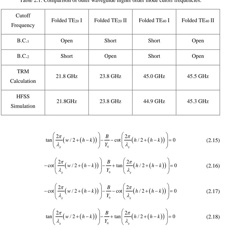
Table 2.1: Comparison of outer waveguide higher order mode cutoff frequencies. Cutoff
Frequency Folded TE20 I Folded TE20 II Folded TE40 I Folded TE40 II
B.C.1 Open Short Short Open
B.C.2 Short Open Short Open
TRM Calculation 21.8 GHz 23.8 GHz 45.0 GHz 45.5 GHz HFSS Simulation 21.8GHz 23.8 GHz 44.9 GHz 45.3 GHz
(
)
(
)
(
(
)
)
0 2 2 tan / 2 cot / 2 0 g g B w h k h h k Y π π λ + − − − λ + − = (2.15)(
)
(
)
(
(
)
)
0 2 2 cot / 2 tan / 2 0 g g B w h k h h k Y π π λ λ − + − − + + − = (2.16)(
)
(
)
(
(
)
)
0 2 2 cot / 2 cot / 2 0 g g B w h k h h k Y π π λ λ − + − − − + − = (2.17)(
)
(
)
(
(
)
)
0 2 2 tan / 2 tan / 2 0 g g B w h k h h k Y π π λ + − − + λ + − = (2.18)The choice of the boundary conditions can be confirmed by observing each higher order mode field distribution shown in Figure 2.8, where maximum E field implies open and minimum E filed implies short. By solving the above nonlinear equations under each boundary condition, each higher order mode cutoff frequency can be calculated. To demonstrate the proposed TRM method, the calculated cutoff frequencies of the higher order modes are compared to the simulated dispersion curves as shown in Table 2.1. The calculated and simulated results with HFSS agree
very well with each other within the variation less than 0.5%. This method provides an accurate prediction for the upper limit of the monomode frequency region of the outer waveguide.
The cutoff frequencies of inner waveguide higher order modes are relatively easy to calculate due to its similarity to the rectangular waveguide or SIW. In our case, the waveguide width is much large than the height, and the first several higher order modes are all TEn0 modes (n=2, 3, 4…). Therefore, the inner waveguide cutoff frequencies can be calculated by:
0 2 n c n f w µε = (2.19)
where n is the mode index and w is the waveguide width.
2.3.2 Monomode Frequency Region
It is always desirable to have a monomode frequency operation for both the inner and outer waveguides, where all the higher order modes are not propagating. Based on the higher order modes analysis above, the monomode frequency region of the outer waveguide ranges from DC to its first higher order mode cutoff frequency fc_folded_TE20, while that of the inner waveguide ranges from its fundamental mode cutoff frequency fc_TE10 to the first higher order mode cutoff frequency
fc_TE20. The frequency region from fc_folded_TE20 to fc_TE10 is denoted as the monomode forbidden region where no monomode propagation can be achieved in either waveguide.
To show each of the mentioned regions, MCW with the same specifications in the previous analysis is re-used here with 0.508 mm thick RT/duroid 6002 substrate. When w=2.54 mm, the outer waveguide monomode frequency region is from DC to fc_folded_TE20=21.8 GHz, and the inner waveguide monomode frequency region is from fc_TE10=34.4 GHz to fc_TE20=68.8 GHz. In this case, the monomode forbidden region is from 21.8 GHz to 34.4 GHz, where the higher order mode starts to show up in the outer waveguide while frequency is still below the cutoff frequency of the inner waveguide. This monomode forbidden region will change as w changes as shown in Figure 2.11. When the w/h ratio increases, the monomode forbidden region reduces correspondingly.
For the MCW constructed with the same substrates in both waveguides, it always holds that
fc_folded_TE20 is smaller than fc_TE10, regardless of the choice of their dimensions. The existence of the monomode forbidden region is inevitable if the substrate permittivity is constant across the whole structure. However, there are some possible ways to narrow down or even eliminate the forbidden
region at the cost of using different permittivity substrates and increasing fabrication complexity. These methods can be either to bring down fc_TE10 by increasing the permittivity of the inner waveguide or to push up fc_folded_TE20 by decreasing the permittivity of the outer waveguide. The physical implementation of these methods is not discussed here.
Figure 2.11: Calculated monomode regions for the inner and outer waveguides at different width.
2.4 Fabrication of Mode Composite Waveguide
The MCW in this thesis is fabricated using three layers of PCB substrates with multiplayer substrate integrating technique, which is made available in our Poly-Grames Research Center. The fabrication process uses middle layer to construct the inner waveguide and all three layers to construct the outer waveguide of MCW as shown in Figure 2.12, following the four steps below:
• Step I: Choose the middle substrate with its thickness equal to the height of the inner waveguide. Metalize the top and bottom surfaces of the substrate to form the top and bottom metallic covers of the inner waveguide.
• Step II: Insert via arrays at the middle substrate along the propagation direction to form the side walls of the inner waveguide and the inner conductor of the outer waveguide.
• Step III: Glue the top and bottom substrates to the middle substrate to form the triple layer MCW structure. Metallize the top and bottom surfaces of the structure to form the top and bottom metallic covers of the outer waveguide.
• Step IV: Insert via arrays at the triple layer MCW structure along propagation direction to form the side walls of the outer waveguide.
Figure 2.12: Fabrication process of the substrate integrated MCW
The above-described four steps define structural and electrical constrains and limits, which should be considered to achieve a desired performance, starting from the substrate and size selections (permittivity and thickness) to the choice of the metalized via parameters (shape, dimension and position). Of course, the fabrication of a MCW depends on the processing techniques. In some cases, the bilateral walls of the inner waveguide can be synthesized with continuous metallic walls. In the above theoretical analysis, the substrate via effects are assumed to be negligible provided that the design of such via arrays meets the requirement of substrate integrated side walls without leakage.It worth to mention that, this concept of MCW is not only
limited to substrate integrated technique, and other technologies such as LTCC, RF CMOS and 3D printing can also be used for fabrication.
2.5 Dimension of Mode Composite Waveguide
According to the previous parametric study, the choice of substrate and dimensions for MCW is a tradeoff in impedance, loss, operation frequency, and fabrication complexity. To achieve the optimal performances of both inner and outer waveguides, the width, height and permittivity of MCW shall be carefully chosen. Due to the substrate integration nature, the height and permittivity of MCW are determined by the substrate property in use, which is limited by its market availability. Also, the total thickness of the multilayer circuit is limited by our laboratory fabrication process to be less than 2.54 mm (100 mil) for prototyping. Compared to the height and permittivity restrictions, the choice of the MCW width is much more flexible, which only depends on the inner and outer waveguide vias positions in design. After tradeoff analysis with performance, robustness, fabrication and cost, we use three layers of 0.508 mm thick RT/duroid 6002 substrates (εr=2.94) to
construct the MCW, where the inner waveguide is built on the middle layer and the outer waveguide is built on all three layers.
The dimensions of substrate integrated MCW are shown in Figure 2.13, where the heights of the inner and outer waveguides are Hi=0.508 mm and Ho=1.524 mm respectively, based on the substrate selection. The width of inner and outer metalized vias are Wvi=0.254 mm and Wvo=0.762
mm respectively, where the outer via is three times wider than the inner counterpart due to the fabrication restriction that via width shall be at least half the substrate total thickness for metallization purposes. The metal width of the inner waveguide is also slightly extended by
Wmc=0.254 mm to meet the via metallization requirement in our laboratory. The side gap distance
Wg=0.508 mm is selected such that both the vertical and horizontal gap distances between the inner
and outer conductors are kept the same. Instead of using circular vias, the rectangular vias are used in the thesis to achieve better accuracy in waveguide width control. Both the inner and outer waveguide vias are periodic with length Lv=2.286 mm and gap Lg=0.254 mm. The via gap is the
minimum allowable size in fabrication, to minimize the gap leakage loss.
The dimensions of MCW selected above will be used in all the circuits in this thesis, unless otherwise mentioned, and the inner waveguide width Wi will be the only parameter that differs in different applications. According to the previous inner waveguide analysis, the inner waveguide width Wi is directly related to its fundamental mode cutoff frequency. Though the parameter Wi can be arbitrarily chosen according to the circuit designer, the choice is crucial to determine the operating frequency of inner waveguide. Therefore, based on the inner waveguide operation band in each MCW circuit implementation, the optimal Wi can be selected accordingly. This selection of substrate and related dimensions will be applied to all the following MCW circuits in this thesis.
2.6 Conclusion
In this chapter, the inner and outer waveguides of MCW are analyzed respectively using the mode isolation property of MCW. The key waveguide parameters such as propagation constants, impedances, losses, and higher order mode cutoff frequencies of both the inner and outer waveguides of MCW are analyzed. Equations are summarized for each waveguide parameter of MCW respectively. Parametric study is conducted using simulation and calculation results, where the effects of different MCW parameters are presented. The MCW dimension selection is discussed based on the parametric study, and the corresponding fabrication process is also provided.
CHAPTER 3
JOINT FEEDING NETWORK OF MODE COMPOSITE
WAVEGUIDE
To measure the MCW or connect the MCW to other planar circuits, guiding signal in the proposed MCW need to be transitioned to planar transmission lines such as microstrip line or CPW. The standalone transitions of inner and outer waveguides to microstrip line are first presented, respectively. Then two types of joint feeding networks of MCW are presented, which can excite both the inner and outer waveguides from different microstrip line feedings simultaneously.
3.1 Outer Waveguide Feeding Network
The outer waveguide is fabricated on a triple layer structure, where the inner conductor is sandwiched between the top and bottom layers. To match the triple layer outer waveguide to the single layer microstrip line, a multilayer transition with various tapering structures is designed (shown in Figure 3.1).
In this demonstration, the inner waveguide width Wi=2.54 mm is selected for the MCW. This
transition can match both the impedance and field distribution at the same time, where their gradual changes at each denoted cross section are also shown in Figure 3.1. The field distribution of microstrip line (P1) which is mostly confined in the first layer is gradually converted to the field distribution of the outer waveguide (P4), where the fields are symmetrically distributed in all the three layers. The transition cross sections of P2 and P3 in between P1 and P4 are also shown here, exhibiting a smooth evolution of both the impedance and field distribution. The design parameters of the outer waveguide to microstrip line transition are Wms=1.321 mm, Wt1=3.556 mm, Wt2=0.762
mm, Lt=8.763 mm, and the total MCW length is Ltot=13.21 mm as shown in Figure 3.1. The total
length of tapering structure is dependent on the operation frequency, where a longer taper is needed when the circuit is operating at a lower frequency band.
The fabricated microstrip line to outer waveguide transition in back-to-back is shown in Figure 3.2. TRL calibration is used to de-embed the connector effect in the two-port measurement. The simulated and measured results are in a good agreement as shown in Figure 3.3. Good matching of the transition for low frequency operation is achieved from 7 GHz to 13 GHz (S11<-10dB), and total insertion loss (including two back-to-back transitions and a certain length of outer waveguide) is better than -0.6 dB in the operation band.
Figure 3.1: 3D view, dimensions of microstrip line to outer waveguide transition in back-to-back setup, and the E field distributions and impedances at each denoted position.
(a)
(b)
Figure 3.2: Pictures of the front side (a) and back side (b) of the fabricated MCW with microstrip to outer waveguide transition.
Figure 3.3: Simulated and measured S-parameters of the back-to-back microstrip line to outer waveguide transition.