TOWARDS NEAR-INFRARED PHOTOSENSITIZATION OF TUNGSTEN TRIOXIDE NANOSTRUCTURED FILMS BY UPCONVERTING NANOPARTICLES
FRÉDÉRIC VENNE
DÉPARTEMENT DE GÉNIE PHYSIQUE ÉCOLE POLYTECHNIQUE DE MONTRÉAL
MÉMOIRE PRÉSENTÉ EN VUE DE L’OBTENTION DU DIPLÔME DE MAÎTRISE ÈS SCIENCES APPLIQUÉES
(GÉNIE PHYSIQUE) JUILLET 2015
c
ÉCOLE POLYTECHNIQUE DE MONTRÉAL
Ce mémoire intitulé:
TOWARDS NEAR-INFRARED PHOTOSENSITIZATION OF TUNGSTEN TRIOXIDE NANOSTRUCTURED FILMS BY UPCONVERTING NANOPARTICLES
présenté par: VENNE Frédéric
en vue de l’obtention du diplôme de: Maîtrise ès sciences appliquées a été dûment accepté par le jury d’examen constitué de:
M. PETER Yves-Alain, Doctorat, président
Mme SANTATO Clara, Doctorat, membre et directrice de recherche M. MOUTANABBIR Oussama, Ph. D., membre
DEDICATION
ACKNOWLEDGMENTS
Foremost, I would like to thank Prof. Clara Santato for accepting me into her research group, and providing me a highly stimulating opportunity. Thanks for your remarkable availability, scientific rigor, and constant support. I would also like to thank the members of the jury, Prof. Oussama Moutanabbir and Prof. Yves-Alain Peter, who kindly accepted to review this master’s thesis.
I would like to thank my close collaborators on this project, Prof. Fiorenzo Vetrone, and Dr. Marta Quintanilla, for their expertise and scientific contribution. I acknowledge the work done by Dr. Dilek Isik, a former graduate student in the group who started the investigation on upconverting nanoparticles a few years ago. I would also like to thank Dr. Bill Baloukas and Hubert Camirand for the discussions we had on tungsten trioxide, and Yves Drolet, Francis Boutet, Jean-Paul Lévesque, Joël Bouchard, and Christophe Clément for the technical support. You are magicians: research would not work without you. Thanks also to Patricia Moraille for the help with the atomic force microscope, and Jeremy Lerner (president at LightForm, Inc) for fruitful discussions about the hyperspectral imaging system.
A thought goes to the Santato’s team and all the people working in room PJAB-3076. Thanks Eduardo, Jonathan, Francis, Xuri, Tian, Shiming, and Xiang for the convivial atmosphere, and support (scientific or moral!). I would like to show my gratitude to the visiting students for the stimulating discussions: Kestutis, Martin, and Gustavo. Some people that are now gone, but still marked my master’s experience: Julia, Sareh, and Umar. Thanks also to the people working in Prof. Fabio Cicoira’s research group (Prajwal, Olga, Irina, Zhihui) for providing me valuable comments on presentations made during joint group meetings. Thanks also to the several summer students in the group. Please acccept my apologies for not remembering all your names.
I would like to thank the coffee addicts Jean-Hughes, Joseph, and Martin for the stimulating and interesting discussions we had around the coffee machine. Thanks to Christian Majeau for his cheerfulness: it is always a pleasure to meet you at the lobby at the beginning of a day. I would like to thank my family for teaching me that hard work and education are the motor of change. I owe a lot to N. Cartier: I never said thank you for the toolbox. My thoughts go to my old friends: Jess, Peter, Déric, Félix, and Maxime.
Enfin, j’aimerais adresser quelques mots en français à la femme qui m’accompagne et me supporte depuis les sept dernières années. Merci Audrey pour ton soutien, ta patience et présence: je t’aime et n’y serais jamais arrivé sans toi.
RÉSUMÉ
Les semiconducteurs à base d’oxydes de métaux nanostructurés sont des matériaux dont l’étude est largement répandue dans le domaine des applications solaires, tel que le démontre l’engouement pour les cellules solaires de type Grätzel. L’oxyde de tungstène (WO3) est un
matériau qui a des propriétés électrochromiques et possède une énergie de bande ≈ 2.5 eV, ce qui lui a permis d’être étudié dans des applications reliées à la conversion (photocatalyse ou photoélectrochimie) de l’énergie solaire. Cependant, la valeur de l’énergie de bande du WO3 est telle qu’il est transparent pour une grande partie du spectre solaire, ce qui limite
l’efficacité de conversion de puissance des dispositifs à base de WO3.
Les matériaux à conversion ascendante de photons sont des matériaux qui peuvent absorber plusieurs photons de faible énergie et émettre un photon de haute énergie. Notamment, les nanoparticules à conversion ascendante de photons sont grandement étudiées pour leur capacité à tranformer deux ou plusieurs photons infrarouge en un photon visible, dans des domaines tels que les applications biomédicales et de l’énergie solaire. En ce qui a trait aux applications en énergie solaire, une partie importante du spectre solaire est composée d’infrarouge, donc de photons qui ont une énergie trop faible pour générer une paire électron-trou dans un semiconducteur à large bande interdite, tel que le WO3. Les nanoparticules à
conversion ascendante de photons sont donc d’intéressantes candidates pour transformer la lumière infrarouge en lumière qui puisse être utilisée par des semiconducteur à grande énergie de bande, tels que les oxydes de métaux.
Ce projet de maîtrise consiste à ajouter des nanoparticules à conversion ascendante de photons (NaGdF4:Er3+, Yb3+) à un oxyde de métal nanostructuré, à savoir le WO3. De cette façon,
l’objectif est d’augmenter l’efficacité de conversion de puissance du WO3 lorsqu’exposé à la
lumière solaire. L’intégration des deux nanomatériaux est motivée par le contact intime qui peut s’établir entre eux, dans le but de potentiellement optimiser leur interaction.
L’article 1 inclus dans le mémoire concerne des nanoparticules de NaGdF4:Er3+, Yb3+mélangées
à du WO3 en phase liquide pour le dépôt de couches minces nanocomposites sur un substrat
composé d’une paire d’électrodes faite de verre conducteur (ITO). Après avoir optimisé les paramètres de préparation et de dépôt des couches minces, ces dernières ont été systématique-ment caractérisées. La morphologie a été étudiée à l’aide de la microscopie à force atomique, la structure à l’aide de la diffraction de rayons-X, les propriétés de photoluminescence à l’aide d’un microscope hyperspectral à fluorescence et les propriétés électriques par des mesures de courant en fonction du temps sous irradiation infrarouge. Principalement, nous observons
une augmentation du courant dans les couches minces composées de NaGdF4:Er3+, Yb3+ et
WO3 lorsqu’elles sont exposées à de la lumière infrarouge par rapport au courant dans le
noir, ce qui est attribué à la production d’un photocourant. Nous émettons l’hypothèse que les photons émis par le laser à 980 nm sont probablement absorbés par les nanoparticules à conversion ascendante de photons et convertis en lumière visible qui peut être collectée par le WO3, générant ainsi un photocourant.
ABSTRACT
Nanostructured metal oxides semiconductors are widely used in solar energy related appli-cations, such as in dye-sensitized solar cells. Tungsten trioxide (WO3) is an electrochromic
material, extensively investigated in solar energy conversion (e.g. photoelectrochemistry) and conservation (e.g. electrochromism). However, WO3, because of its wide bandgap (≈ 2.5 eV),
is transparent to an important portion of the solar spectrum and can effectively absorb light only up to ca. 500 nm, which limits the power conversion efficiency of devices based thereon. Upconverting materials can absorb several low-energy photons to emit one high-energy pho-ton. In particular, upconverting nanoparticles are widely studied in biomedical and solar energy applications, as they can transform two or several infrared photons in a visible pho-ton. As the Sun contains important NIR and IR portion, UCNPs are interesting candidates to transform NIR or IR light into visible light to be absorbed by wide bandgap semiconductor, such as metal oxides.
The work presented in this master’s thesis consists in embedding NaGdF4:Er3+, Yb3+
UC-NPs into a nanostructured WO3 matrix. The objective is to increase the power conversion
efficiency of WO3 after solar light harvesting. The integration of two materials with
nanos-tructured nature has the potential to lead to a good synergy between them.
We include an article in this master’s thesis. In this article, we report on the mixing of NaGdF4:Er3+, Yb3+UCNPs with WO3in solution and on the deposition of the two-component
solution on ITO-patterned electrodes. After engineering the fabrication and deposition of the thin nanocomposite films, they were systematically studied. Morphology was studied by atomic force microscopy, structure by X-ray diffraction, photoluminescence by fluorescence hyperspectral microscopy, and charge carrier transport under NIR irradiation by current-time measurements. Notably, we observed an increase in the value of the current with respect to the dark current when UCNP/WO3 thin films were exposed to 980 nm continuous
laser irradiation. This increase in the value of the current is tentatively attributed to the absorption of the NIR light by the UCNPs, which is upconverted into visible light to be harvested by the WO3, eventually generating a photocurrent.
TABLE OF CONTENTS
DEDICATION . . . iii
ACKNOWLEDGMENTS . . . iv
RÉSUMÉ . . . v
ABSTRACT . . . vii
TABLE OF CONTENTS . . . viii
LIST OF FIGURES . . . xi
LIST OF ACRONYMS AND ABBREVIATIONS . . . xv
LIST OF APPENDICES . . . xvi
CHAPTER 1 INTRODUCTION AND LITERATURE REVIEW . . . 1
1.1 Solar energy conversion . . . 1
1.1.1 Solar cells . . . 3
1.1.2 Beyond Shockley–Queisser limit . . . 5
1.1.3 Metal oxides in solar energy conversion . . . 7
1.1.3.1 TiO2: a paradigmatic example . . . 7
1.1.3.2 WO3 . . . 8
1.1.4 Upconversion process as a strategy to photosensitize metal oxides . . 9
1.1.4.1 Upconversion: origin and mechanisms . . . 9
1.1.4.2 Synthesis of UCNPs . . . 11
1.1.4.3 Internal quantum yield of lanthanide-based UCNPs . . . 12
1.1.4.4 Application of UCNPs to solar cells . . . 13
1.2 Problem definition . . . 14
1.3 Objective of the work . . . 15
1.4 Plan of the thesis . . . 15
CHAPTER 2 EXPERIMENTAL SECTION . . . 16
2.1 Materials . . . 16
2.1.1 WO3 synthesis . . . 16
2.1.3 Fabrication of the thin films . . . 18
2.2 Microfabrication of the electrodes . . . 18
2.2.1 General remarks . . . 18
2.2.2 Microfabrication process . . . 19
2.3 Characterization . . . 21
2.3.1 Photoluminescence properties of UCNPs . . . 21
2.3.2 X-ray diffraction . . . 22
2.3.3 Atomic force microscopy . . . 22
2.3.4 Electrical measurements in dark and light conditions . . . 24
CHAPTER 3 ARTICLE 1: TOWARDS NEAR-INFRARED PHOTOSENSITIZATION OF TUNGSTEN TRIOXIDE NANOSTRUCTURED FILMS BY UPCONVERTING NANOPARTICLES . . . 25
3.1 Authors . . . 25
3.2 Abstract . . . 25
3.3 Introduction . . . 26
3.4 Experimental section . . . 27
3.4.1 Microfabrication of the electrodes . . . 27
3.4.2 Materials and fabrication of the thin films . . . 27
3.4.3 Characterization . . . 28
3.5 Results and discussion . . . 29
3.5.1 Thin film preparation and characterization . . . 29
3.5.2 Electrical Measurements . . . 33
3.6 Conclusions and perspectives . . . 35
3.7 Acknowledgements . . . 35
3.8 Supplementary information to article 1 . . . 36
3.8.1 Authors . . . 36
3.8.2 Supplementary information . . . 36
CHAPTER 4 COMPLEMENTARY RESULTS . . . 39
4.1 Choice of the configuration . . . 39
4.2 Effect of the thermal treatment temperature on UCNPs photoluminescence properties . . . 40
4.3 Effect of the UCNPs size . . . 41
4.4 Towards a better understanding of the results presented in article 1 . . . 43
4.4.1 Current-time measurements of 8 mol % UCNP/WO3 thin films under white light . . . 43
4.4.2 Current-time measurements of 8 mol % UCNP/WO3 thin films under
chopped light at variable frequency . . . 44
4.4.3 Temperature-dependent current-time measurements of 8 mol % UCNP/WO3 thin films under chopped light . . . 45
4.5 Results on LiYF4: Tm3+, Yb3+ UCNPs . . . 46
CHAPTER 5 GENERAL DISCUSSION . . . 49
CHAPTER 6 CONCLUSIONS AND PERSPECTIVES . . . 51
6.1 Conclusions . . . 51
6.2 Perspectives . . . 52
BIBLIOGRAPHY . . . 53
LIST OF FIGURES
Figure 1.1 Spectral distribution of Sun’s irradiation [1]. . . 2 Figure 1.2 Bandgap structure of a semiconductor. The bandgap energy (Eg)
corre-sponds to the energy difference between the edges of the conduction(Ec)
and valence band (Ev). . . 3
Figure 1.3 a) Losses mechanisms inside a solar cell [2]: (1) Thermalization, (2) Opical transparency, (3) Electron hole recombination, (4) Loss at the p-n junction and (5) Contact losses. b) Maximum achievable power conversion efficiency vs bandgap energy in SQ scenario [3]. . . 6 Figure 1.4 Diagram for the three major mechanisms by which upconversion may
occur. Reproduced from [2]. . . 11 Figure 1.5 Lumiscence measurement setup to evaluate the efficiency of UC
mate-rials. Reproduced from [4]. . . 12 Figure 2.1 Process flow of the synthesis of WO3. In the first step, an aqueous
solution of Na2WO4 is passed through a proton-exchange resin. Then,
H2WO4 is collected in ethanol. After the evaporation of the solvent,
an organic stabilizer (PEG-200) is added. As prepared sols could be used within 72 h. . . 17 Figure 2.2 Illustration of the synthesis of UCNPs. After the preparation of the
precursors, lanthanides trifluoroacetates are injected in oleic acid and octadecene at 315◦C, before aging for 1 h at constant temperature. Image produced by Dr. Marta Quintanilla. Printed with permission from the creator. . . 18 Figure 2.3 AFM topographical image of ITO substrate, as purchased from
Col-orado Concept Coating. Root mean square roughness (RRMS) is about
5.4 nm (area is 2 × 2 µm). . . . 19 Figure 2.4 Optical microscope image of the patterned electrodes prior to the
chem-ical wet etching step. . . 20 Figure 2.5 Microfabrication steps for planar ITO-patterned electrodes. . . 21 Figure 2.6 AFM working principle. A sample is placed under a silicon tip attached
to a cantilever. Depending on the operating mode, the tip can be in contact or touch the sample intermittently. The deflection of the cantilever allows to obtain information on the topography of the sample investigated. Reproduced from [5]. . . 23
Figure 2.7 Comparison of the two operating modes. In contact mode, the sample and the tip are in contact, and the deflection of the cantilever is pro-portionnal to the forces acting on the tip. In tapping mode, the tip oscillates near the surface at a given frequency, resulting in a change of the amplitude of oscillation and force between the tip and the sample. 23 Figure 2.8 Setup for the electrical measurements. WO3 or UCNP/WO3 thin films
were deposited on patterned substrates. A constant bias was applied, and the current was measured over time. . . 24 Figure 3.1 (a) TEM image of β-NaGdF4:Er3+, Yb3+ UCNPs. (b) Experimental
configuration adopted for the electrical characterization (photocurrent vs time). Topographical AFM images of (c) WO3 and (d) 8 mol%
UCNP/WO3 films, deposited on glass, treated at 385◦C. (e) PL
spec-trum of β-NaGdF4:Er3+, Yb3+UCNPs drop-cast on glass and thermally
treated at 385◦C (right y axis) and optical transmission spectrum of a WO3 film (≈1 µm in thickness), deposited on glass and thermally
treated at 385◦C (right y axis). Inset figure 3.1(e): PL spectrum of the UCNPs, drop-cast on glass and dried at room temperature. . . 31 Figure 3.2 XRD patterns of β-UCNPs, 45 nm in diameter, drop-cast on glass.
After room temperature drying and thermal treatment at 385◦C, UC-NPs are in the β-phase (hexagonal phase, patterns 1 and 2). The peak positions for the α and β phases are included at the bottom of the figure [6]. . . 32 Figure 3.3 Current-time measurements under NIR chopped light (60 s in the dark
and 30 s under irradiation, λexc=980 nm, power density=1 W/cm2) for
films deposited on patterned ITO with an interelectrode distance of 100 µm and thermally treated at 385◦C made of (a) 8 mol% UCNP/WO3
and (b) WO3 (see figure 3.7). Samples were kept under constant
elec-trical bias for 300 s in ambient light conditions, followed by 300 s in the dark, before chopping the light. . . 34 Figure 3.4 Optical microscope images of 16 mol% UCNP/WO3 films thermally
Figure 3.5 Partial NaGdF4:Er3+, Yb3+ UCNPs energy levels diagram.For the sake
of clarity, only the energy levels involved in the upconversion process are shown. Dashed lines are associated to energy absorption, dotted lines are associated to energy transfer, full grey lines are associated to non-radiative processes, and full double lines are associated to radiative processes. . . 37 Figure 3.6 XRD measurements of WO3 (pattern 1) and 8 mol % UCNP/WO3
thin films deposited on glass substrate and thermally treated at 385◦C (pattern 2). . . 37 Figure 3.7 Current-time measurements of pure WO3 thin films thermally treated
at 385◦C deposited on patterned ITO with an interelectrode distance of 100 µm under LED white light (Thorlabs, model LIU004). Initially the sample was kept in dark conditions for 300 s at an applied electrical bias of 1 V, followed by 300 s under LED white light, followed by dark conditions. . . 38 Figure 4.1 Two configurations investigated at the beginning of the project. a)
“Layered” configuration: the UCNPs are deposited on a WO3 thin
film. b) “Nanocomposite” configuration: the UCNPs are embedded in the WO3. . . 39
Figure 4.2 PL properties of a) hexagonal b) cubic phase UCNPs deposited on WO3 (full lines). The PL properties of a thin film made from pure
UCNPs (dashed lines), drop-cast on a glass substrate are also shown for reference. . . 40 Figure 4.3 PL intensity of pure hexagonal UCNPs treated at different
tempera-tures. Size of the UCNPs is 35 nm. UCNPs dispersed in water were drop-cast on a glass substrate and thermally treated at RT, 400◦C, and 550◦C. Green emission is strongly affected by the temperature of the thermal treatment. . . 41 Figure 4.4 Current-time measurements of thin film samples deposited on
sub-strates patterned with ITO electrodes and thermally treated at 400◦C. The samples were kept under electrical bias (V=0.7 V) for 5 min in ambient light conditions followed by 5 minutes in the dark before chopping the light (λexc=980 nm). Nanocomposite films containing
8 mol %UCNPs/WO3 with (A) 35 nm-sized hexagonal UCNPs and
Figure 4.5 Current-time measurements of UCNP/WO3( 8 mol %) thin films
ther-mally treated at 385◦C deposited on patterned ITO with an interelec-trode distance of 100 µm under white LED light (Thorlabs, model LIU004). Samples were kept under constant electrical bias (1 V) for 300 s in dark conditions, followed by 300 s under white LED light, followed by dark conditions. An increase in current is observed when the white LED is shed on the sample. . . 43 Figure 4.6 Current-time measurements under NIR chopped light for ≈ 8 mol %
UCNP/WO3. Thin films were deposited on patterned ITO with an
in-terelectrode distance of 100 µm and thermally treated at 385◦C. Sam-ples were kept under constant electrical bias for 300 s in ambient light conditions, followed by 300 s in the dark. Frequency of chopping light was 1 Hz and 0.5 Hz, respectively. . . 44 Figure 4.7 a) Temperature-dependent current-time measurements under NIR chopped
light (λexc=980 nm, power density ≈ 5 W/cm2) for 8 mol % UCNP/WO3.
Thin films were deposited on patterned ITO with an interelectrode distance of 100 µm and thermally treated at 385◦C. b) Table show-ing the evolution of the substrate temperature and the on/off ratio R. Temperature-dependent current-time measurements at c) T1=50◦C, d)
T2=45◦C, e) T3=40◦C and f) T4=35◦C. . . 46
Figure 4.8 TEM image of LiYF4: Tm3+, Yb3+ UCNPs. This image was collected
by Dr. Marta Quintanilla (INRS-EMT, Prof. F. Vetrone’s research group). . . 47 Figure 4.9 Photoluminescence properties of LiYF4: Tm3+, Yb3+UCNPs, drop-cast
on a glass substrate and dried at RT. . . 47 Figure 4.10 XRD pattern of the LiYF4: Tm3+, Yb3+ powder. The peaks are
in-dexed to the hexagonal phase [6]. This measurement was performed by Dr. Marta Quintanilla (INRS-EMT, Prof. F. Vetrone’s research group). 48 Figure 4.11 Current-time measurements under NIR chopped light (λexc=980 nm,
power density ≈1 W/cm2) of LiYF4: Tm3+, Yb3+/WO3 thin films
deposited on patterned ITO electrodes (L = 100µm) and thermally treated at 385◦C. . . 48
LIST OF ACRONYMS AND ABBREVIATIONS
AFM Atomic Force Microscopy a-Si Amorphous Silicon c-Si Crystalline Silicon CW Contiuous Wave
DSSCs Dye-Sensitized Solar Cells Ec Conduction band energy level
Eg Bandgap energy
ESA Excited State Absorption ETU Energy Transfer Upconversion Ev Valence band energy level
eV Electronvolt
IR Infrared
IPA Isopropyl Alcohol ITO Indium Tin Oxide η Power Efficiency NIR Near-infrared PA Photon Avalanche
PARISS Prism And Reflector Imaging Spectroscopy System Pdensity Power density
PL Photoluminescence PV Photovoltaics
QY Quantum Yield
TEM Transmission Electron Microscopy
TW Terawatts
UC Upconversion
UCNPs Upconverting Nanoparticles VOC Open-circuit Voltage
LIST OF APPENDICES
Appendix A Theoretical estimation of the photocurrent generated in 8 mol % NaGdF4:
CHAPTER 1 INTRODUCTION AND LITERATURE REVIEW
The discovery of the photovoltaic effect is attributed to Edmond Becquerel, the French sci-entist who studied the effect of light on electrolytic cells. He observed an electric current between two platinum electrodes covered by photosensitive materials, such as AgCl or AgBr, immersed in an acidic solution (such as dilute sulfuric acid) when one electrode was irradi-ated by solar light [7]. It took about a century to reach the development and production of devices that convert light into electricity of any technological interest from the viewpoint of energy conversion efficiency. This improvment in the efficiency was stimulated by the space programs of the 1960s, and above all by the energy crisis of the 1970s [8].
In 2010, the global energy consumption was about 10 terawatts (TW), and recent estimations claim that, by 2050, approximately 30 TW of energy will be required annually to fulfill human-related activities [9]. Among other possibilities, solar energy has the potential to meet this requirement. Indeed, solar power arriving at Earth’s surface is about 120 000 TW, which is approximately 10 000 times more that we actually need [10]. However, to meet the never stopping increase in energy demand, it is mandatory to have technologies that permit to produce highly efficient solar cells. In order to reach the efficiency required for satisfying the energy demand, numerous challenges are still to be addressed.
The Sun is a star that emits light with an extended range of wavelengths that can be approx-imated by a blackbody at a temperature of about 5800 K, which emits from the ultraviolet (UV) to the visible (VIS) and the infrared (IR), with a maximum located around 500 nm. However, the atmosphere protecting the Earth affects the spectral emission of the sun: the UV is partly absorbed by the ozone, H2O absorbs the emission at about 900, 1100, 1400,
1900 nm, and CO2 absorbs at about 1800 and 2600 nm. The position of the Sun also has an
effect on terrestrial irradiation, accounted by the air mass (AM) coefficient, which represents the optical path length of Sun’s irradiation. It can be approximated by AM≈ 1/ cos φ, where φ is the angle of elevation of the Sun with respect to the normal to the Earth’s surface. The standard Sun’s spectrum is named AM1.5 (φ = 48.2◦) [11]. The spectrum of the light that irradiates the Earth’s surface is presented on figure 1.1 [1].
1.1 Solar energy conversion
Now that we know what Sun’s irradiation looks like on Earth’s surface, we can try to fig-ure out how we can use this incoming light. The absorption of photons that results in the
Figure 1.1 Spectral distribution of Sun’s irradiation [1].
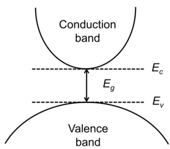
generation of charge carriers can take place in semiconductor materials. An important char-acteristic of semiconductors is the bandgap, namely the difference in energy between the edges of the valence and conduction bands. Figure 1.2 shows the band structure of a typical semiconductor. It is composed of a valence band whose top edge is associated to the energy Ev, and a conduction band, whose bottom edge is located at the energy Ec. The valence
band is usually filled with electrons, so as the electrons cannot significantly move into the material, while the conduction band is empty. The energy difference between the valence and conduction band edges is the bandgap (Eg) and is expressed by equation 1.1:
Conduction band Valence band Eg Ec Ev
Figure 1.2 Bandgap structure of a semiconductor. The bandgap energy (Eg) corresponds to
the energy difference between the edges of the conduction(Ec) and valence band (Ev).
When a photon hits a semiconducting material, one of the following situations occurs: 1. The photon is absorbed by the semiconductor, and an electron-hole pair is generated; 2. The photon is transmitted by the material. In this case, the semiconductor is
“trans-parent” to the photon;
3. The photon is reflected by the surface of the semiconductor.
In the first situation, the energy of the incoming photon has to be at least Eg. As a result,
an electron is liberated from its bound state and is promoted to the conduction band, such as it can move and contribute to the current. When an electron is promoted to the con-duction band, it leaves an ‘empty space’ behind. This space is an absence of electron, and can therefore be seen as a particle with a positive charge (hole) that can move within the material [12].
In the second situation, the energy of the incoming photon cannot be effectively used by the semiconductor to generate charge carriers. Several approaches are feasible to improve the light harvesting properties of a semiconductor: some of them are presented in section 1.1.4. An anti-reflection coating is normally placed on top of PV device in order to avoid the third situation, namely the reflection of the incoming light on the material.
1.1.1 Solar cells
The first class of solar cells investigated during the 1960s were based on III-V (e.g. GaAs [13]) or II-IV semiconductors (e.g. CdTe [14]). Around the same time, the possibility to produce
polycrystalline in industrial quantity came up. As a result of more than 50 years of research and development in the field on silicon-based technologies, the cost of production of energy produced by silicon-based solar cells is now low (ca 3 $/W), and the power conversion ef-ficiency high (about 25 % for c-Si) [11]. This class of solar cells, exclusively based on c-Si, is referred as ‘first generation’ solar cells. It relies on a p-n junction, which is an interface between an n-type (large electrons concentration) and a p-type (large hole concentration) semiconductor (as indicated on figure 1.3 a)). Second generation solar cells are based on thin films technology and use, among others, amorphous silicon (a-Si) or CdTe. They are less efficient than c-Si solar cells, but the advantage of such solar cells is the relatively low cost and the possibility to use a wide range of substrates, such as flexible substrates [15].
In the field of solar energy conversion, the power conversion efficiency η is the ratio of the power that can be extracted from the solar cell to the power irradiating the solar cell, namely:
η = Pout Pin
(1.2)
There are many factors affecting the final efficiency of a solar cell, but the two major power-loss mechanisms in a single-junction solar cell are the inability to absorb photons with energy lower than the bandgap and the thermalization of photons with energy higher than the bandgap. When combined, these two effects are responsible for about 50% of the losses [2]. The two first generations of solar cells are based on a single p-n junction and subject to the Shockley-Queisser (SQ) limit, which is a thermodynamic efficiency limit that is related to the value of the bandgap of the semiconductor [3]. The SQ limit relies on several assumptions. First, when a photon with an energy higher than Eg is absorbed by the semiconductor, the
excess of energy is transformed into heat, which creates phonons. Then, every electron and hole that do not recombine diffuse to their respective electrodes to be eventually extracted. The only allowed recombination mechanism takes place via radiative process. Also, it is supposed that the photoactive material is thick enough to harvest as much light as possible at a certain wavelenght. It was also assumed that the Sun is a blackbody at 6000 K, that one photon generates one electron-hole pair, and that photons with energy below the bandgap do not generate an electron-hole pair. The calculations of the theoretical maximum power that can be extracted from a single p-n junction lead to the two following conclusions [3]:
1. The optimal bandgap is located for a single-junction solar cell at around 1.2 eV; 2. The highest efficiency attainable for a device based on a material with Eg = 1.2 eV is
These two conclusions are also illustrated on figure 1.3 b).
It is now appropriate to present what is called ‘third generation photovoltaics’. The goal of third generation PV is to overcome the Shockley–Queisser limit, preferably at low cost. A broad range of possibilities has been proposed to overcome this limit, and every possibility aims at either changing the design of the solar cell or the light harvested by the solar cells. Third generation PV is still at a research level, and is not ready yet for commercialization. The next section will illustrate how it is possible to overcome the limit inherent to single junction solar cells.
1.1.2 Beyond Shockley–Queisser limit
Among the many feasible possibilities aiming at attaining solar cells with power conversion efficiency higher than the SQ limit, four categories can be identified, namely: multi-junction cells, intermediate-band cells, hot carrier cells and spectrum conversion [15].
Multi-junction cells or ‘multiple energy level approach’ refers to the possibility of using sev-eral energy gaps to absorb different wavelengths and portions of the solar spectrum. This approach was first proposed by Jackson in 1995, and it consists in stacking p-n junctions with different materials (i.e. with different bandgaps), such as the material with the high-est bandgap absorbs first the light [16]. Being transparent to higher wavelenghts, the rhigh-est of the light is absorbed by subsequent p-n junctions with lower bandgaps [17]. They can be monolithically integrated, i.e. made from several layers put in mechanical and electrical contact, but preparation of such devices is challenging, because the electrical characteristics of each layer have to be matched, without what electrons can be absorbed by a layer without being collected. Four-junction solar cells are to this day the devices with the highest efficency reported (ca. 46%, measured at a concentration of 508 suns, Fraunhofer, 2014).
The second approach presented is the ‘intermediate-band cells’. This strategy consists in introducing at least one energy level within the bandgap of the photoactive material, e.g. by incorporating an impurity. Historically, the first two examples reported in the literature are the addition of B in SiC and In in Si [18, 19]. However, the addition of impurities in a solar cell also increases the probability of radiative and nonradiative recombination. If this approach appears interesting in theory, no experimental work has shown that it could indeed increase the efficiency of the solar cell [18].
The third approach is based on the idea of using ‘hot carriers’, i.e. carriers generated by a photon with an energy higher than Eg. It was proposed in 1982 by Ross and Nozik [20].
(a) (b)
Figure 1.3 a) Losses mechanisms inside a solar cell [2]: (1) Thermalization, (2) Opical trans-parency, (3) Electron hole recombination, (4) Loss at the p-n junction and (5) Contact losses. b) Maximum achievable power conversion efficiency vs bandgap energy in SQ scenario [3].
an electron-hole pair whose energy can be higher than the bandgap energy [15]. After a relative small amount of time (≤ 1 ps), the hot carriers will relax, thus transferring their excess of energy to the lattice of the semiconductor, which results in the production of optical phonons, namely oscillation of the lattice resulting in a vibrating motion. These phonons will interact with other phonons, and the energy in excess of the bandgap will be simply lost. The major concept behind this approach consists in slowing down (>> ps) the transformation of the extra energy of the photogenerated carriers into phonons, such as these hot carriers could be collected. However, experimental implementations of this idea is somehow limited, and much of the work has been made from a computational point of view. In this perspective, theoretical calculations estimated that efficiencies of about 80 % are attainable in solar cells usings hot carriers and concentrated sunlight [21]. One instance of this general approach is called ‘multiple carrier excitation’. It also relies on the use of carriers generated from high-energy photons (Ehν ≥ Eg). The mechanism involved in this process is still not completly
understood, but it is believed that carriers generated with high-energy photon can undergo impact ionization, which allows creating several electron-hole pairs [15]. To this day, the most efficient system in which this phenomenon occurs is based on quantum dots (QDs), where up to seven electron-hole pairs can be created by the absorption of one photon. It has been shown in PbSe QDs, but also in II-VI semiconductors and silicon-based QDs [22, 23]. The last approach herein presented, namely the spectrum conversion, consists in modulating the incoming light. The main goal of this approach is to make a better use of Sun’s spectrum by transforming the incoming light such as it becomes usable by the semiconductor material. Several optical processes can be used, the most relevant being: quantum cutting (QC),
down-shifting (DS), and upconversion (UC). Quantum-cutting refers to the process where a material absorbs one high energy photon and re-emits two (or more) low energy photons. Down-shifting is an optical process where one high-energy photon is absorbed by a material, that after non-radiative relaxation, emits one photon having a fraction of the energy of the initial photon. A brief overview on QC and DS fundamental aspects and applications can be found in [24]. In the UC process, two (or more) low energy photons are subsequently absorbed by a material that can then emit a photon with higher energy [25]. The use of the UC process definitely fits into the ‘third generation’ solar cells approach: fundamental considerations and applications in PV devices will be presented in section 1.1.4.
1.1.3 Metal oxides in solar energy conversion
The aim of this section is to present how metal oxides have been used in solar energy conver-sion. One of the most cited examples is the use of metal oxides in dye-sensitized solar cells (DSSCs)1. DSSCs are based on a dye-coated semiconductor (e.g. TiO
2) and an electrolyte
sandwiched between two transparent electrodes. The seminal work published by O’Reagan and Grätzel showed that it was possible to attain 7 % efficiency in a DSSC [29]. Since then, a considerable amount of work have been made towards the development of DSSCs with high efficiency. For the sake of clarity and concision, we will not explain with great details the working principle of DSSC and will rather focus on semiconductors used in these cells, more specifically nanostructured metal oxides [29]. This example of solar cells shows advantages over the classic p-n junction, such as: their convenient synthesis route, low cost, thermal stability and tunability.
1.1.3.1 TiO2: a paradigmatic example
The idea of photosensitizing a material with a relatively wide bandgap dates back in the 1970s, and scientists were at that time motivated by the investigation of photoelectrochemical pro-cesses [30]. In the 1970s, photoelectrochemical devices based on metal oxide photoelectrodes (e.g. ZnO) had an efficiency of ca. 1%, and the first use of dye-sensitized nanostructured TiO2 in photoelectrochemical devices was reported by Deb in 1978 [30, 31, 32]. Then, the
research slowly moved towards the use of semiconductors with narrow bandgap such as Si. The key behind the finding made by O’Reagan and Grätzel that prompted renewed interest in the DSSCs approach was the use of mesoporous metal oxides electrodes, i.e. metal oxides
1Metal oxides are also used in other solar energy conversion devices, such as quantum-dots and organic
solar cells. For the sake of concision and clarity, we will not discuss these approaches, but these topics are covered in [26, 27] (for QDs solar cells) and [28] (for organic solar cells).
containing nanometric size pores. Notably, the surface area of mesoporous metal oxides is estimated to be 1000 times higher than a bulk thin film. As a result, there is a better interac-tion between the dye and the semiconductor, which enhances the light harvesting properties of the cells.
TiO2 is a stable metal oxide that is widely used in a broad range of applications, such
as pigment or sunscreen. It can exist in several crystal structures, such as the anastase and rutile structures. Most of the research done during the last twenty years aimed at developing different synthesis routes and nanostructures (e.g. nanoparticles, nanowires). It can be produced by several ways, such as sol-gel, hydrothermal, chemical vapor deposition, physical deposition and electrodeposition [33]. Among others, the enhancement of the charge carrier transport properties, and the minimization of charge recombination have been widely investigated in TiO2. TiO2 is still, to this day, the semiconductor that is mostly used to
produce nanostructured electrodes for DSSCs.
1.1.3.2 WO3
In this section the emphasis will be put on WO3, a semiconductor with a large bandgap (ca
2.5 eV). The bandgap of this material is more suitable than TiO2(Eg ≈ 3.2 eV) from the solar
light application point of view. Indeed, unlike TiO2 that absorbs only in the UV region of
the solar spectrum, WO3 can absorb wavelenght up to 500 nm [34]. Apart from its bandgap,
WO3 has many interesting features for technological applications. It can indeed be obtained
in various crystalline structures, nanostructured, mesoporous, transparent to a large portion of the solar spectrum and synthetized by many different synthesis routes, including sol-gel, hydrothermal, anodization methods, sputtering, chemical vapor deposition [35, 36].
This material is also widely studied for its electrochromism properties, which means that it can undergo a reversible change in color under electrical bias. Thanks to this property, WO3
finds application in security devices and smart windows [37].
Several works have reported the use of solar energy conversion devices based on WO3. For
example, it has been used as hole blocking layer in OPV and photoanodes. As it is resistant against corrosion and can withstand aqueous acidic conditions, it has also been used for water splitting applications and photoelectrochemistry [38].
Recently, a lot of research has been going on to nanostructure WO3, which could enhance the
properties of the material. Among others, strategies consist in increasing the surface/volume ratio (which could result in a greater surface area for chemical reactions to take place) or reducing the size to benefit from quantum confinement effects [39].
1.1.4 Upconversion process as a strategy to photosensitize metal oxides
From what has been said in section 1.1.2, one possible way to go beyond Shockley-Queisser limit is to ‘transform’ the light before it reaches the material. In this section, the UC process is first presented from a theoretical point of view to illustrate why upconverting materials are interesting to photosensitize metal oxides.
1.1.4.1 Upconversion: origin and mechanisms
The origin of upconversion procress can be traced back in 1959, when Bloembergen proposed to make use of rare Earth salts in order to be able to detect infrared photons. As he pointed out, lanthanide-doped materials have a rich energy level diagram [40]. This phenomenon (up-conversion) was then first observed by Auzel in 1966 [41]. There are two classes of materials in which upconversion can take place. First, UC process can take place in lanthanides or transi-tion metal ions hosted in an inorganic material and, secondly, in organic chromophores [42]. As the work done for this thesis is stricly concerned with lanthanides-based UCNPs, the focus will be put on the mechanisms associated with this class of upconverting materials. Lanthanides are 15 elements with [Xe]6s24fn electronic configuration, where n represents
the number of electrons in the 4f orbital, and 0 ≤ n ≤ 14 [2]. The partial filling of the 4f orbital is responsible for the unique optical and magnetic properties of the lanthanides-based UCNPs. The completly filled 5s and 5p orbitals act as a shield, thus protecting the 4f orbital from the environment. These two characteristics explain why UCNPs exhibit sharp optical emission, and relatively long lifetime for their excited states (ranging from µs to ms) [43]. Since 4fn transitions are Laporte-forbidden2 in order to preserve the dipole
moment, there is only a small probability of transition, which results in long excited state lifetime [44]. If n represents the number of electrons in 4f orbitals, there are 14n possible electronic configurations: it explains the rich energy level diagram of lanthanides.
In particular, NaGdF4:Er3+, Yb3+ UCNPs are known to be one of the most efficient UC
system (the ratio of the number of emitted photons to the number of absorbed photons varies from 0.005 % to 3 % depending on the size and crystalline phase of the UCNPs) and have been widely investigated [4, 45]. Their high efficiency can partly be explained by the choice of the host material. The fluoride host is a material of choice, because it has low lattice phonon energy, which considerably reduces the probability of non-radiative processes [46, 44]. Fluoride hosts are also very stable from a chemical viewpoint. The main 2Laporte selection rule states that electronic transitions that preserve parity are not allowed. It applies to
atoms and molecules with an inversion center. Then, electronic transitions that conserve parity are unlikely to take place within centrosymmetric atoms and molecules.
features of the doping materials are the rich and ladder-like energy level diagram of Er3+
and the simple energy diagram of Yb3+. Yb3+ only has two states: one ground state and one excited state [47]. In the case of NaGdF4:Er3+, Yb3+ UCNPs, the emission of light is
the results of the interaction between two ions. Yb3+ with its high absorption cross-section
and short lifetime absorbs the NIR photons and transfers them to Er3+, that can absorb two
low energy photons before emitting one high energy photon. Some of the limiting factors for efficient emission are the distance between the two emitting ions and the absorption cross-section [48]. NaGdF4:Er3+, Yb3+UCNPs are interesting because they can easily be produced,
and their size and phase can be tuned [44].
Upconversion may occur thanks to three working mechanisms: excited-state absorption (ESA), energy transfer upconversion (ETU), and photon avalanche (PA) (represented on figure 1.4) [44]. In the ESA mechanism, a single ion with ladder-like energy levels sequen-tially absorbs two (or more) photons to reach an excited state. Once in its excited state, a radiative process may occur. As seen on figure 1.4, a single ion absorbs a photon that is resonant with the energy gap between its ground (G) and excited state (E1). After absorbing
this photon, the ion is in its first excited state (E1). Now, let us assume there exists a second
excited state E2, such that E1− G = E2− E1. It means that if another photon is absorbed
by the materials, the ion will be promotted to E2, which could result in a radiative relaxation
(from E2 to G). In the cases where E1− G 6= E2− E1, the ion has to be irradiate with several
light sources with different wavelengths [45].
ETU requires that two types of ion, a sensitizer and an activator, are placed in proximity (few Å) in a host material [41]. This case has partly been introduced with the NaGdF4:
Er3+, Yb3+ UNCPs. In this type of upconversion process, a photon with an energy resonant
to the energy gap between the ground state and the excited state of the sensitizer (e.g. Yb3+)
is absorbed, which promotes the ion to its excited state. The same process occurs in an-other sensitizer. Then, a non-radiative energy takes place betwen the first sensitizer and the activator (e.g. Er3+), which allows the activator to be promoted to its first excited state
(E1). Following this, the second sensitizer involved in this process transfers its energy to
the activator, which promotes the activator from its first excited state to its second excited state (from E1 to E2). After the energy transfer, both sensitizer ions relax to their ground
state, and the upconversion occurs from the E2 level to the ground state of the ion [2]. A
number of conditions have to be met in order for the upconversion to take place by ETU: the absorption cross-section of the sensitizer has to be high, the energy level spacing of the sensitizer and the activator has to be resonant, and the activator has to have ‘long’ life-time (normally ranges from 10 µs to 10 ms ) [44]. As a rule of thumb, the ion concentration of the sensitizer is at least 10 times higher that the activator. ETU is often reported as the
most efficient process, and its main advantage over other optical processes (e.g. two-photon absorption) is the need of a low power laser source (as low as 1 W) [41].
PA is a mechanism that explains that upconversion can occur in a material above a threshold power of irradiation. Basically, it is a process where ESA process and cross-relaxation are both involved. The first excited state (E1) of an ion is populated, followed by a resonant ESA
that promotes the ion to E2. Then, a cross-relaxation energy transfer takes places between
this ion and another ion in its ground state, promoting the second ion to an excited state E1.
This energy is then transferred to the first ion, which populates its E1 level. In the end, two
ions are at level E1, and one of them can absorb a photon and be promoted to E2. Again,
a cross-relaxation process can take place with another ion in the ground state, which results in three ions at E1 level. By repeating these steps several times, the E2 level of an ion can
easily be populated, which results in a strong emission [2].
Figure 1.4 Diagram for the three major mechanisms by which upconversion may occur. Re-produced from [2].
1.1.4.2 Synthesis of UCNPs
UCNPs can be produced in many different ways, which allows to control, among others, their chemical composition, size, morphology, structure, and emissive properties. Many synthesis routes have been reported in the literature, such as: thermal decomposition, hydrothermal, co-precipitation, microwave-assisted, and ionic-liquid based synthesis [44]. As the synthesis of UCNPs is a field of research on its own, we will not give here a complete overview on the
topic 3. The synthesis route adopted in the case of this master’s thesis is based on a thermal
decomposition process that will be presented in section 2.1.2.
1.1.4.3 Internal quantum yield of lanthanide-based UCNPs
A few works have been done on the characterization of the effficiency of UC materials [4, 49], which is accounted by the internal quantum yield (QY). QY is defined by equation 1.3 and corresponds to the ratio of the number of emitted (upconverted) photons over the number of photons absorbed by the UCNPs.
Internal QY = #photons emitted
#photons absorbed (1.3)
The vast majority of the work published focus on lanthanide-based UCNPs. The first paper on systematic investigation of the QY of UCNPs was published by Boyer and van Veggel in 2010 [4]. They designed an experimental setup for measuring the QY of UCNPs using a spectrophotometer, an integrating sphere, and a continuous wave (cw) 980 nm laser diode. Using their setup, the authors were able to report that the QY of green emission in NaYF4:
Er3+, Yb3+ is ranging from 0.005 % to 3 %, depending on the phase and the size of the
nanoparticles. The experimental setup is shown on figure 1.5.
Figure 1.5 Lumiscence measurement setup to evaluate the efficiency of UC materials. Repro-duced from [4].
1.1.4.4 Application of UCNPs to solar cells
Even if UC materials have been extensively studied in the last decades, it took approximately thirthy years after the discovery made by Auzel before seeing the first application of UC materials in solar energy. More specifically, the first use of lanthanides ions for solar cells can be traced back to 1996, when Gibart et al. reported the use of a 100 µm-thick Er3+/Yb3+
co-doped ceramic on the rear of a GaAs solar cell [50]. Before incorporating the co-doped ceramic layer in the solar cell, the authors were able to observe the UC green and red emissions attributed to Er3+ion upon 891 nm illumination. They also observed that the response of the
solar cell depends quadratically with the input power of the laser source, which supported that a two-photon process was taking place in their system. However, the authors concluded that the efficiency of GaAs solar cell at 891 nm (Pdensity= 25 W/cm2) of about 2.5% was too
low for any practical applications.
Trupke et al. were the first to publish a theoretical work on the possibility to improve solar cell efficiency by UC materials. Most notably, they reported on different geometries for c-Si solar cells and illumination conditions in order to show that the maximum efficiency attainable by UCNPs/c-Si is about 48% for non-concentrated light. This number increases up to 63.2 % for concentrated sunlight (about 46,000 suns) [51].
Historically, and following the development of well-established microelectronic processes and technologies, solar cells based on crystalline silicon were first extensively studied. It took almost ten years following the work made by Gilbart et al., for the community to start to use Er3+-based UCNPs with crystalline silicon (c-Si) solar cell. The first example of this kind
of work can be found in Shalav et al. [52]. In this pioneering work, they used NaYF4: Er3+
UCNPs dispersed in a transparent acrylic medium that was attached to the rear of a bifacial c-Si cell. Under IR radiation (λ = 1523 nm, from a 5.1 mW laser), a quantum efficiency of 2.5% was reported. The work done by Liang et al. is an interesting example of a work using less conventionanal UC materials. The authors proposed to make use of Gd2(MoO4)3: Er3+.
This nanophosphor is able, upon 1500 nm irradiation (power density ≈ 700 W/m2), to emit
light at 545, 665, 800, ans 980 nm, i.e. wavelengths that could be absorbed by crystalline silicon (Eg=1.1 eV or 1130 nm) [53].
Following the same historical pattern as in the solar cells field, UCNPs were subsequentlyused for amorphous silicon (a-Si) based solar cells. However, its larger bandgap compare to c-Si (1.75 vs. 1.1 eV) makes it more sensitive to transmission losses. The two first papers on the photosentization of a-Si solar cells by UCNPs were published by Wild et al [54, 55]. Indeed, they reported on the use of NaYF4:Er3+, Yb3+ in a thick transparent layer placed at the
enhancement in current of about 6 %, which corresponds to an external quantum efficiency (the ratio of the number of charge carriers collected to the number of incident photons) of 0.03 % for the solar cell.
In 2010, the first work demonstrating the possibility to integrate UCNPs in DSSC solar cells was published by Shan and Demopoulos [56]. In this work, the authors synthesized 10 nm sized LaF3: Er3+, Yb3+ UCNPs to produce an upconverter/TiO2 nanocomposite layer
deposited on conducting glass (FTO) that was used as a working electrode. The overall effi-ciency of the solar cell under AM1.0 solar irradiation was about 2.7%, which was comparable to the efficiency of the solar cell without any UCNPs. This low efficiency was attributed to the inefficient absorption of the red upconverted light by the dye and the charge carrier recombination at the nanocomposite/electrolyte interface. Several papers have recently been published on the use of UCNPs in DSSCs [57, 58, 59, 60, 61]. Recently, several reviews have focused on the use of UCNPs in photovoltaics [62, 43, 63, 64].
1.2 Problem definition
Now that the theoretical background and the relevant literature on the topic have been sufficiently covered, it is possible to explicitly state the definition of the problem investigated during this project. First, this project makes use of a mesoporous, nanostructured solution-processed metal oxide, WO3, that has been intensively studied in electrochromics as well as
in solar energy conversion (photocatalysis and photoelectrochemistry). This material has a large bandgap of ca. 2.5 eV, which means that it is optically transparent for an important portion of the solar spectrum. It is clear that if one is interested to effectively use this material in solar energy conversion applications, it is necessary to extend its solar light absorption properties to NIR and IR portions of the solar spectrum. UCNPs are materials that can convert two (or several) low-energy photons into one high-energy photon. A possibility to overcome the limited spectral response of WO3 could be the concomitant use of WO3 and
UCNPs. As seen in section 1.1.4, most of the work done in the field of using UC materials in solar cell consists in integrating a layer containing UCNPs on the rear face of the solar cells and to use a mirror to reflect the upconverted light back into the cell. The advantage of this approach is clear: in this fashion, it is possible to integrate the UC material without altering the design of commercially produced solar cells. Indeed, the addition of the UC layer only adds one step to the process, and the solar cells can be produced by the same industrial process. Using nanometric UC materials with nanostructured WO3 could allow a
better contact between the two materials, which could potentially increase the interaction between the two materials without the help of a mirror. Also, it could enable the possibility
to produce one layer containing metal oxide that is sensitive to the visible and NIR portions of the solar spectrum, thanks to the interaction between UCNPs and WO3. Then, combining
UCNPs with nanostructured WO3 is an appealing approach to extend the spectral response
of the semiconductor towards the NIR portion of the solar spectrum. It has been discussed in the previous section that nanostructured solution-processed metal oxides are interesting for many reasons. They are easy to produce in crystalline or amorphous forms, and are suitable for applications in photoelectrochemistry and electrochromism. In this context, lanthanide-based UCNPs can theoretically be used to photosensitize WO3 in the NIR region of the solar
spectrum.
1.3 Objective of the work
Our objective was to enhance the absorption properties of nanostructured solution-processed tungsten trioxide thin films to extend its light harvesting properties towards the NIR portion of the solar spectrum. This research question has been organised into three specific objectives that have been adressed in this master’s thesis:
1. Develop a procedure that permits to synthesize thin films containing a known UCNPs/WO3
ratio;
2. Characterize the uniformity and roughness of the thin films in order to assess their possible integration in solar energy conversion devices.
3. Evaluate the impact of the addition of UCNPs in WO3 on the electrical photoresponse
of WO3;
1.4 Plan of the thesis
This master’s thesis is separated in the following manner:
1. Chapter 2 presents the experimental techniques and methods used in this work; 2. Chapter 3 is the reproduction of an article submitted to RSC Advances in June 2015; 3. Chapter 4 contains complementary results, not included in the article, that are useful
to a better understanding of the results; 4. Chapter 5 presents a general discussion;
CHAPTER 2 EXPERIMENTAL SECTION
This chapter is separated into three sections. First, we describe how the materials were prepared. Then, we explain how the substrates where the materials are deposited were fabricated by microfabrication. Finally, we present the working principle of the experimental setup for the characterization methods.
2.1 Materials
In this first section, we present the synthesis routes of the materials under investigation (WO3
and NaGdF4:Er3+, Yb3+ UCNPs). Then, we present how the thin films were fabricated.
2.1.1 WO3 synthesis
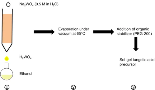
WO3 was prepared following a sol-gel synthesis reported in the literature [65]. Basically,
Na2WO4 salt (Sigma Aldrich) was dissolved in water to obtain a solution of 0.5 M
concentra-tion and the obtained aqueous soluconcentra-tion was passed through a proton-exchange resin (Dowex 50WX2, Sigma Aldrich). This resin has the property to substitute Na+ with H+ ion, such
as H2WO4 solution can be collected. It is important to collect this solution in a solvent,
e.g. ethanol, to slow down the condensation of tungstic acid [66]. The solution is always maintained under continuous magnetic stirring. After partial evaporation of the solvent with a rotavapor, an organic stabilizer is added to the tungstic acid. The stabilizer used was poly(ethylene glycol)-200 (PEG-200), and WO3/PEG-200 ratio was ≈ 0.5 w/w. The
result-ing viscous, yellow sol could be used within 72 h, whereupon a precipitate was formed. The synthetic route is schematically illustrated in figure 2.1.
2.1.2 Upconverting nanoparticles synthesis
The synthesis of the UCNPs has been conducted by Dr. Marta Quintanilla at INRS-EMT (group of Prof. F. Vetrone). The synthetic route to prepare upconverting nanoparticles al-lows to control the nanoparticle size, morphology, and crystalline phase [44]. A thermal decomposition synthesis that relies on the decomposition of fluoride precursors of lanthanide ions at high temperature was adopted. NaGdF4:Er3+, Yb3+UCNPs were prepared via a
ther-mal decomposition process already reported in the literature [67]. In the process, lanthanide trifluoroacetates, used as precursors, were prepared from lanthanide oxides (Alpha Aesar, Gd2O3, Er2O3, Yb2O3, >99.99%) dissolved in deionized water and trifluoroacetic acid
(Al-Na2WO4 (0.5 M in H2O) H2WO4 Ethanol Evaporation under vacuum at 65°C Organic stabilizer (PEG-200)
1
2
3
Addition of organic stabilizer (PEG-200)Sol-gel tungstic acid precursor
Figure 2.1 Process flow of the synthesis of WO3. In the first step, an aqueous solution of
Na2WO4 is passed through a proton-exchange resin. Then, H2WO4 is collected in ethanol.
After the evaporation of the solvent, an organic stabilizer (PEG-200) is added. As prepared sols could be used within 72 h.
pha Aesar, 99%). The obtained precursors, together with the required stoichiometric amount of sodium trifluoroacetate (Sigma-Aldrich, 98%), were injected at a rate of 1.0 mL/min in a 1:1 solution of oleic acid (Alpha Aesar, 90%) and octadecene (Alpha Aesar, 90%) at 315◦C and aged for 1 h. Oleic acid acts as the coordinating ligand, and octadecene as the reaction solvent. The role of the reaction solvent is to have a high boiling point solution, so as the decomposition of the fluoride precursors of lanthanide can occur.
The as prepared NaGdF4:Er3+, Yb3+ UCNPs were then washed by centrifugation and
re-dispersed in hexane. As synthesized, UCNPs are capped with oleic acid, i.e. they are hydrophobic. Oleic acid was removed thus rendering the UCNPs hydrophilic by a process reported in the literature [68]. The final UCNPs were normally ≈ 45 nm in diameter.
Figure 2.2 Illustration of the synthesis of UCNPs. After the preparation of the precursors, lanthanides trifluoroacetates are injected in oleic acid and octadecene at 315◦C, before aging for 1 h at constant temperature. Image produced by Dr. Marta Quintanilla. Printed with permission from the creator.
2.1.3 Fabrication of the thin films
First, a mixture made from 1% weight/weight concentration of UCNPs suspension in water and ca. 0.3 M WO3 solution was prepared and aged for at least 1h under continuous stirring.
Several UCNPs/WO3 mol % ratios from 2 to 16 mol % UCNP/WO3 were investigated.
Thin films were obtained from drop-casting 10 µL of WO3 or UCNP/WO3 solution on
ITO-patterned substrates, followed by a thermal treatment at 385 ◦C under the presence of O2
(160 standard cubic centimeters per minutes) for 30 min.
2.2 Microfabrication of the electrodes
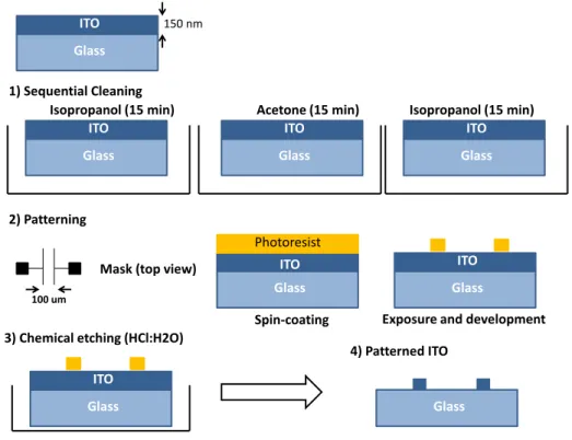
We fabricated planar devices in order to investigate the electrical properties of our thin films. Electrodes were patterned fromITO-coated glass (L = 100 µm, and width W = 6000 µm). The fabrication steps are detailed in sections 2.2.1 and 2.2.2.
2.2.1 General remarks
Microfabrication processes are commonly used to produce devices with micrometric dimen-sions, e.g. in microelectronics, and can usually be separated into three steps: photolithogra-phy, etching, and deposition. Microfabrication can be done on a wide variety of substrates, such as silicon wafers and glass. Photolithography is required to define patterns on the substrate. Basically, a photoresist, i.e. a polymer mixed with a photoactive component, is spin-coated on a substrate. Afterwards, the substrate is exposed through a photomask to UV light. When the patterns contained on the mask are exposed to a UV lamp, the exposed
portion of the photoresist covering the substrate becomes soluble or insoluble in a developer: in the former case, the photoresist is said to be ‘positive’, while it is said to be ‘negative’ in the latter case. After the development of the photoresist in a developer, patterns are trans-ferred on the photoresist. Etching is used to selectively remove a portion of the film from the substrate. It can be achieved using several methods, such as plasma and wet eching. Then, deposition techniques can be used to add a layer on the device.
2.2.2 Microfabrication process
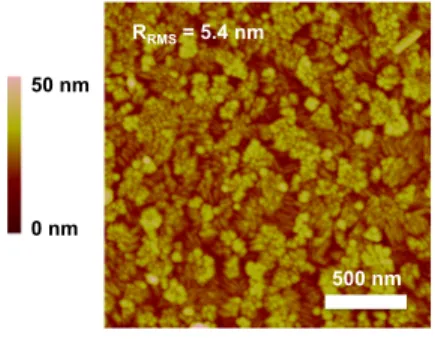
In the case of the work done during this master’s thesis, the microfabrication process consists in two steps only: photolithography and etching. We used microfabrication to pattern ITO-covered glass (30 mm x 30 mm, <15 Ω/square, purchased from Colorado Concept Coating). An AFM image of a typical ITO substrate is shown on figure 2.3. Prior to the microfabrication step (process flow is indicated on figure 2.5), the substrate were sequentially cleaned in an ultrasonic bath of isopropyl alcohol (IPA) for 15 min, acetone for 15 min, IPA for 15 min, and dried with a N2 flux. Then, the substrates were exposed to a UV-ozone treatment for 15 min,
in order to remove the organic contaminants from the surface. Substrates were immediately taken to the clean room to proceed to the microfabrication step.
Atomic force microscopy - substrate
ITO-coated glass 13 / 25 500 nm RRMS = 5.4 nm 50 nm 0 nm
Figure 2.3 AFM topographical image of ITO substrate, as purchased from Colorado Concept Coating. Root mean square roughness (RRMS) is about 5.4 nm (area is 2 × 2 µm).
Prior to the photolithography step, the substrates were placed into a Yield Engineering Systems Oven for 15 minutes for a dehydratation process under vacuum. When the substrate was cooled at room temperature, a positive photoresist (SPR 220 3.0) was spin-coated at 3000 rpm for 40 s to achieve a photoresist final thickness of about 3 µm. Then, the substrate was cured with a softbake at 115◦C for 90 s. When the substrate was back at room temperature, the photoresist was exposed through a mask to a UV lamp using a Karl Suss MA4 mask aligner. The exposition time was adjusted to provide the optimal UV light dose to the photoresist. The optimal dose was found to be around 23 mJ/cm2. Then, the substrate
underwent a post-exposure bake at 115◦C for 90 s. The substrate was cooled down to room temperature, and after 5 minutes, the photoresist was developed for 3 min 40 s at room temperature using MF319 under continuous stirring.
90 µm
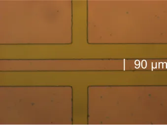
Figure 2.4 Optical microscope image of the patterned electrodes prior to the chemical wet etching step.
Afterwards, chemical wet etching was used to remove the exposed ITO. The substrate was immersed in a hydrochloric acid (HCl) solution (HCl:H2O 65 v/v%) for about 9 minutes,
resulting in ITO-patterned electrodes with an interelectrode distance L = 100 µm, and width W = 6000 µm. Prior to the drop-casting of the solution (WO3 or UCNP/WO3),
ITO-patterned substrates were cleaned again following the sequential procedure that was previously stated. The result of the microfabrication steps is ITO electrodes patterned on top of a glass substrate.
ITO Glass 150 nm 1) Sequential Cleaning ITO Glass ITO Glass ITO Glass
Isopropanol (15 min) Acetone (15 min) Isopropanol (15 min)
2) Patterning
Mask (top view) ITO
Glass
Photoresist
Spin-coating
ITO Glass
Exposure and development 3) Chemical etching (HCl:H2O)
ITO Glass ITO Glass 100 um 4) Patterned ITO
Figure 2.5 Microfabrication steps for planar ITO-patterned electrodes.
2.3 Characterization
In this section, the characterization techniques that were used during this master’s project are presented: photoluminescence, X-ray diffraction, atomic force microscopy, and current-time measurements. The working principles will also be described.
2.3.1 Photoluminescence properties of UCNPs
Photoluminescence is the property some material has to emit light after the absorption of photons. In our case, we were intrerested in obtaining the photoluminescence spectrum of UCNPs. To do so, we excited the UCNPs with the proper wavelength to detect the light emitted by UCNPs after the upconversion process. Fluorescence hyperspectral imaging was used. The microscope can be used with a lamp source whose emission spectrum is close to a mercury lamp spectrum. During our experiments, light source was a portable continuous wave (cw) NIR laser emitting at 980 nm.
Photoluminescence measurements were achieved with Prism And Reflector Imaging Spec-troscopy System (PARISS, purchased from LightForm Inc.) in ambient air condition and temperature under a 980 nm cw laser excitation. The PARISS system was used
concomi-tantly with a microscope (Olympus BX-51) spectrometer, a CCD camera, and a software (PARISS 8.0) to record the photoluminescence spectrum.
2.3.2 X-ray diffraction
X-ray diffraction permits to characterize the crystalline phases of a sample. First, an X-ray beam irradiates a sample, and is diffracted by the crystallographic planes of the sample. Then, the difference in the optical path caused by the reflection on the plane allows the beam to interfere with the beam reflected by other planes. It leads to the observation of constructive interference peaks, following the Bragg equation:
nλ = 2d sin θ
In our experiments, the crystalline structure of the UCNPs, WO3, and UCNPs/WO3 samples
were performed in a Bruker D-8 Advance Diffractometer using CuKα radiation.
2.3.3 Atomic force microscopy
Atomic force microscopy (AFM) is a widely used characterization technique which permits obtaining topographical information of a sample. Working principle, as illustrated on fig-ure 2.6, relies on the measfig-urement of the deflection of the cantilever. Atomic force microscope is made of a feedback loop and a cantilever with a nanometric size silicon tip (tip radius ≈ 10 nm) at the end. AFM can be operated into two modes (figure 2.7). The first one is called ‘contact mode’, meaning that the tip is in contact with the sample. A constant force, corresponding to the deflection setpoint, is applied, such as the only allowed deflection is attributable to a change in the topography of the surface. This mode cannot be used with soft or fragile materials and is known to easily damage the tip. The second mode is the ‘tapping mode’. It allows to circumvent the listed disadvantages of the contact mode. In this case, a force is applied to the end of the cantilever, such that the tip oscillates near the surface of the sample. When the tip is close to the surface, the amplitude of the oscillation reduces, and the tip is in contact with the sample for a short amount of time. The deflection of the cantilever is measured with a laser beam in the visible that is reflected by the tip to a photodetector. An acquisition software is used to record three dimensional images of a sample surface. The size of these images is variable and generally ranges between 1 and 100 µm. Once the topographical image is recorded, it is possible to obtain information on the surface under investigation, such as the profile, the roughness, the depth of holes, and size of the particles. A second image, called ‘phase image’ is also collected: it is the result of
a change in oscillation frequency of the cantilever during the scanning of the sample. This image can provide information on the physical and chemical properties of a sample. For example, it is possible to distinguish between two different materials on a phase image, but it is not possible to identify what exactly are the materials. One can only say that the two materials are different.
Figure 2.6 AFM working principle. A sample is placed under a silicon tip attached to a cantilever. Depending on the operating mode, the tip can be in contact or touch the sample intermittently. The deflection of the cantilever allows to obtain information on the topogra-phy of the sample investigated. Reproduced from [5].
Contact mode
Non-contact mode
Intermittent contact mode
Probe-sample distance Force R ep ul si ve fo rce s At tra ct ive fo rce s
Figure 2.7 Comparison of the two operating modes. In contact mode, the sample and the tip are in contact, and the deflection of the cantilever is proportionnal to the forces acting on the tip. In tapping mode, the tip oscillates near the surface at a given frequency, resulting in a change of the amplitude of oscillation and force between the tip and the sample.
.
Every AFM image produced in this work was obtained in ambient air condition using a Veeco Dimension 3100 Digital Instruments with Si cantilever (tip radius < 10 nm, spring constant 40 N/m) at a scan rate of 1 Hz in tapping mode.
![Figure 1.1 Spectral distribution of Sun’s irradiation [1].](https://thumb-eu.123doks.com/thumbv2/123doknet/2351083.36280/18.918.225.670.114.486/figure-spectral-distribution-of-sun-s-irradiation.webp)
![Figure 1.3 a) Losses mechanisms inside a solar cell [2]: (1) Thermalization, (2) Opical trans- trans-parency, (3) Electron hole recombination, (4) Loss at the p-n junction and (5) Contact losses](https://thumb-eu.123doks.com/thumbv2/123doknet/2351083.36280/22.918.114.795.125.342/figure-losses-mechanisms-thermalization-electron-recombination-junction-contact.webp)
![Figure 1.4 Diagram for the three major mechanisms by which upconversion may occur. Re- Re-produced from [2].](https://thumb-eu.123doks.com/thumbv2/123doknet/2351083.36280/27.918.243.705.473.736/figure-diagram-major-mechanisms-upconversion-occur-produced.webp)
![Figure 1.5 Lumiscence measurement setup to evaluate the efficiency of UC materials. Repro- Repro-duced from [4].](https://thumb-eu.123doks.com/thumbv2/123doknet/2351083.36280/28.918.289.606.652.923/figure-lumiscence-measurement-evaluate-efficiency-materials-repro-repro.webp)