O
pen
A
rchive
T
OULOUSE
A
rchive
O
uverte (
OATAO
)
This is an author-deposited version published in : http://oatao.univ-toulouse.fr/
Eprints ID : 19957
To link to this article : DOI:10.1007/s10404-017-1970-z
URL : http://dx.doi.org/10.1007/s10404-017-1970-z
To cite this version : Naillon, Antoine
and Massadi, Hajar and
Courson, Rémi and Bekhit, Jean and Seveno, Lucie and Calmon,
Pierre-François and Prat, Marc
and Joseph, Pierre Quasi-static
drainage in nano-slits network with non-uniform depth designed by
grayscale laser lithography. (2017) Microfluidics and Nanofluidics,
vol. 21 (n° 131). pp. 2-14. ISSN 1613-4982
Any correspondence concerning this service should be sent to the repository
administrator: [email protected]
OATAO is an open access repository that collects the work of Toulouse researchers and
makes it freely available over the web where possible.
Quasi‑static drainage in a network of nanoslits of non‑uniform
depth designed by grayscale laser lithography
A. Naillon1,2,3 · H. Massadi3 · R. Courson4 · J. Bekhit3 · L. Seveno3 · P. F. Calmon3 ·
M. Prat1,2 · P. Joseph3
Keywords Nanofluidics · Porous media · Drainage ·
Nanofabrication · Grayscale lithography · Varying depth 1 Introduction
Immiscible two-phase flows in porous media are encoun-tered in many fields of practical interest, such as petroleum engineering, groundwater hydrology or chemical engineer-ing to name only a few. The literature on the subject is vast and this is still a very active research field, e.g. (Cottin et al. 2010; He et al. 2015; Lee et al. 2015; Jung et al. 2016; Prat 2002) and references therein. Consider the process where a fluid totally occupied the pore space initially and is dis-placed by the injection of another fluid. When the displacing fluid is the wetting phase, the process is called imbibition, whereas drainage corresponds to the displacement of a wet-ting fluid by a non-wetwet-ting fluid (Dullien 1992). In what fol-lows, we are interested in the drainage process. The drainage theory is well established since the 1980s, namely since the work of Lenormand et al. (1988). Considering the situations where gravity effects can be neglected, they showed that the process was essentially controlled by the viscosity ratio of the two fluids and the competition between the viscous and capillary forces. Three main asymptotic regimes, referred to as the capillary fingering regime, the DLA regime and the stable displacement regime, were identified. The stable displacement and DLA regimes, where DLA stands for dif-fusion-limited aggregation (Witten and Sander 1981), cor-respond to regimes where capillary effects are negligible compared to viscous effects, whereas the capillary fingering regime corresponds to a displacement exclusively controlled by capillary effects. This led to a drainage diagram, gener-ally referred to as Lenormand’s diagram, summarizing the main patterns expected in drainage.
Abstract A method is reported to fabricate silicon–glass
nanofluidic chips with non-uniform channel depths in the range 20–500 nm and micrometer resolution in width. The process is based on grayscale laser lithography to structure photoresist in 2.5 dimensions in a single step, followed by a reactive ion etching to transfer the resist depth profile into silicon. It can be easily integrated in a complete pro-cess flow chart. The method is used to fabricate a network of interconnected slits of non-uniform depth, a geometry mimicking a nanoporous medium. The network is then used to perform a pressure step-controlled drainage experi-ment, i.e., the immiscible displacement of a wetting fluid (liquid water) by a non-wetting one (nitrogen). The drain-age patterns are analyzed by comparison with simulations based on the invasion percolation algorithm. The results indicate that slow drainage in the considered nanofluidic system well corresponds to the classical capillary fingering regime.
Electronic supplementary material The online version of this
article (doi:10.1007/s10404-017-1970-z) contains supplementary material, which is available to authorized users.
* P. Joseph [email protected]
1 INPT, UPS, IMFT (Institut de Mécanique des Fluides de
Toulouse), Université de Toulouse, Allée Camille Soula, 31400 Toulouse, France
2 CNRS, IMFT, 31400 Toulouse, France
3 LAAS-CNRS, Université de Toulouse, CNRS, Toulouse,
France
4 Kloe SA, 1068 Rue de la Vieille Poste, 34000 Montpellier,
These results were notably obtained from a series of experiments performed in quasi-two-dimensional model media consisting in square networks of interconnected channels of randomly variable hydraulic diameter. The channel sizes were large, on the order of a few hundred microns. There is, however, no doubt that Lenormand’s diagram also applied in the micrometric range, with pores between 1 and 100 μm in size, (Zhang et al. 2011; Jung et al. 2016).
The situation is less clear as regards the porous materi-als with pores in the nanometric range, which corresponds in this paper to pore sizes between about 10 nm and a few hundred nanometers.
This is an important class to which porous materials such as concrete, mortar, clays and clay rocks belong. The clas-sical approach in engineering is actually to assume that the models used for computing two-phase flows in the micro-metric range, namely the generalized Darcy’s law (Dullien 1992), still applies in the nanometric range. Returning to Lenormand’s approach, this implicitly amounts to assum-ing that the situation with pore sizes in the nanometric range is not significantly different from the one prevailing in systems with bigger pore sizes. However, to the best of our knowledge, this assumption has never been confirmed from visualization experiments on model porous media analogous to the ones performed in the micrometric and submillimeter ranges. This is so because fabricating model systems with pores in the nanometric range is much less straightforward than for bigger sizes, and also because the pattern visualization is also much more difficult when the pore sizes are on the order of the light wavelengths in the visible or even smaller.
Also, recent experimental studies on a simple geom-etry such as single straight channels or slits in the nano-metric range indicate differences with the results valid in micrometric channels. The spontaneous imbibition pro-cess is reported to be slower than predicted by the classi-cal Washburn’s law (1921) (Chauvet et al. 2012; Vincent et al. 2016; and references therein). As reported in Duan et al. (2012), evaporation can be faster than in micromet-ric channels owing to the impact of bubble formation and trapping. Although these processes are not drainage, they are examples of two-phase processes, indicating that the situation in nanometric systems can show differences with the one in systems with bigger pores. It can be noted, how-ever, that the drainage experiments in a system of nanoslits in parallel reported in Wu et al. (2014) do not lead to the identification of significant differences in the flow patterns compared to those observed in conventional-sized tubes. However, this study is limited to flows in straight channels of uniform depth. While investigating flows in individual straight channels is a natural first step, studying the flows in systems of interconnected channels of variable depth is
highly desirable so as to consider pore spaces with geomet-rical properties, such as a distribution in the pore size and the existence of interconnections, closer to the ones exist-ing in real porous media.
In this context, the objective is first to develop a model nanoporous system enabling one to study nanoscale flows in a system of interconnected channels, while permitting visualization using optical microscopy. These two appar-ently contradictory aspects can be met fabricating a net-work of interconnected nanoslits of depth in the 10–100 nm range and width in the micrometric range. This last dimen-sion permits a direct visualization of the two fluid phases in the slits as shown for instance for systems of nanoslits in parallel in Chauvet et al. (2012) or Wu et al. (2014). Fabri-cating a network of interconnected slits is, however, a chal-lenge since standard fabrication techniques typically lead to network of uniform depth (He et al. 2015; and references therein). Since capillary effects are mostly controlled by the smallest dimension of the slit cross section, here the slits depth and not their width, it is crucial that the slits depth varies from one slit to the other in the network. This impor-tant aspect is achieved by adapting grayscale lithography to nanofluidics to get 2.5D nanofluidic networks. Then, the network of interconnected slits is used to perform a quasi-static drainage experiment in order to explore whether the nanoconfinement leads to significant differences com-pared to the classical description presented in Lenormand et al. (1988). The experiments are analyzed by comparison with numerical simulations based on the classical inva-sion percolation algorithm (Wilkinson and Willemsen 1983), which is well adapted to model the capillary finger-ing regime of Lenormand’s diagram, at least again in sys-tems with pore size greater than 1 micron. We focus on the quasi-static regime because this is the conventional regime to compute macroscopic properties of interest, such as the capillary pressure curve or the relative permeabilities, using pore network models (Blunt et al. 2002). However, the nanoporous device presented in what follows could be used in future works for studying the other regimes of Lenormand’s diagram.
2 Development of a direct writing technique to fabricate varying‑depth nanoslits
2.1 Different approaches to fabricate nanoslits with complex depth profile
Standard nanofabrication techniques are intrinsically in two dimensions (2D) because common processes are based on the deposition of thin layers (photoresist or structural mate-rials like metals) followed by their patterning and/or etching (Madou 2011). Consequently, fluidic channels can now be
fabricated down to few nanometers sizes by many methods (Duan et al. 2013), but most of them are in 2D. However, 3D relief opens the path to model media with topologies more representative of a real porous media. More gener-ally, in term of micro- and nanofluidic application, it makes available functionalities not accessible in 2D as the entropic manipulation of DNA (Stavis et al. 2012) or the sorting and characterization of nanoparticles (Stavis et al. 2010).
In this perspective, efforts have been made recently to get nanochannels in 3D. The first class of 3D nanofabrica-tion techniques is based on point-by-point direct writing of each 3D point (voxels) by a very narrow focalization beam, the volume of each written voxel being in the sub-µm3
range. The absence of physical mask makes this approach rapidly reconfigurable and thus good for prototyping. For example, femtosecond laser is often used in manufacturing due to its ability to reach high energy density with limited heating (Sugioka and Cheng 2014). It permits fabricating directly submicrometric channels via optical breakdown (Ke et al. 2005), 50-nm nanochannels buried in glass thanks to nonlinear beam–substrate interaction (Liao et al. 2013), nanotunnels in metal interlayer (Zhang et al. 2013). Femtosecond lasers are also involved in two-photon polym-erization (Sugioka and Cheng 2014) to pattern objects in the 10–100 nm range (Li et al. 2009; Selimis et al. 2015). Another direct writing technique is based on the use of electron-beam (e-beam) or ions. The same type of buried nanochannels as in Liao et al. (2013) have been achieved by Azimi et al. (2014) combining ion beam irradiation, elec-trochemical anodization and high-temperature oxidation.
As a compromise between fully 3D and 2D fabrication, the second group of direct writing methods is based on grayscale lithography (GL), often denoted 2.5D. Its princi-ple is to modulate spatially the exposure dose applied to the resist (Fig. 1a), which permits constructing non-uniform-depth structures in one step. Erdmanis and Tittonen (2014) and Kim et al. (2007) have demonstrated grayscale pattern-ing with e-beam lithography.
The previous approaches, however, involve point-by-point writing of nanovoxels or nanopixels, which are very time-consuming and expensive for wafer-scale processing. To avoid long processing time, two variants of 2.5D meth-ods have been proposed: gray-tone masks and digital micro-mirror device (DMD®) (Totsu et al. 2006; Rammohan et al.
2011; Zhong et al. 2014). In the former, 2.5D fabrication is achieved by using a physical mask whose transparency is not uniform. The variation of optical density can be produced by an array of small diffractive elements (Stavis et al. 2009) or a continuous transparency variation (Wu et al. 2002). It has the advantage to be compatible with simple lithography. However, it suffers from the need of one mask per design (mask cost and fabrication time). Furthermore, its use was only implemented for large structures. In the only example of this method for nanofluidics, Stavis et al. (2009) has fabri-cated channels by gray-tone mask with depth in the few hun-dreds of nanometers range, but with a demonstrated lateral resolution no better than about 100 µm. In digital micromir-ror device (DMD®) technique, a UV light is reflected on an
array of mirrors which can simultaneously insolate different pixels on the substrate. However, the pixel size is around 10 µm (Totsu et al. 2006), and to the best of our knowledge, it was not implemented for nanofluidic applications.
As we discuss in Introduction, many nanofluidic studies need channels with nanometers depth, but can take advan-tage of few micrometers width if the mechanism involved is controlled by the smallest size. Indeed, micrometer width allows a high-throughput analysis and/or it is implemented to use standard optical microscope for observation. In our case, the capillary effects are controlled by the smallest size which imposes meniscus curvature [see Sect. 3.3 and Eq. (1) below]. None of the approaches presented above is fully suited to realize non-uniform-depth nanochannels with micrometer lateral size in a single step. For that purpose, we develop a process, based on grayscale laser direct writ-ing lithography (GLDWL) which fully meets all of those criteria. This maskless technique is ideal for prototyping of
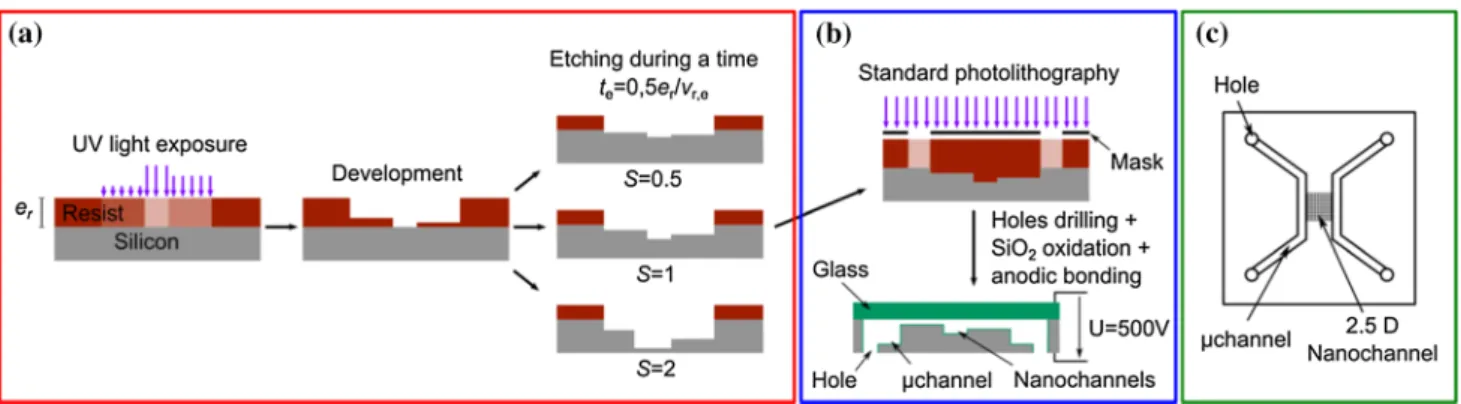
Fig. 1 Flowchart of the fabrication process. a Principle of grayscale laser lithography to fabricate varying-depth nanochannels in one step. b
nanofluidic experiments and fits easily in a standard pro-cess flow. In context of microoptics, GLDWL was reported 20 years ago in the work of Gale et al. (1994) to fabricate microoptical planar elements in positive photoresist. Surpris-ingly, to the best of our knowledge, it has not been adapted to nanofluidics yet. Here, GLDWL is optimized to integrate nanochannels with depths from 20 to 500 nm obtained in a single step, with good lateral resolution (around 2 µm) and low writing time (a few minutes to get a full channel net-work, less than 3 h for a complete four-inch wafer).
In the following sections, we first describe the optimized process and then present the nanofluidic structures fabri-cated in 2.5 dimensions.
2.2 Fabrication process
Nanofluidic chips are realized following the process flow-chart presented in Fig. 1. First, nanochannels with varying depths are structured in a 1.06-µm layer of positive photore-sist AZ ECI 3012 (Microchemicals GmbH), commonly used for binary lithography which needs ~µm spatial resolution. The photoresist is spin-coated on a silicon wafer at 3600 rpm with an acceleration of 5000 rpm/s. The silicon wafer is pre-viously exposed to 800 W O2 plasma during 5 min to ensure its cleanliness and to favor the photoresist adhesion.
UV light exposure is performed with the laser direct writing machine Dilase 750 (Kloé SA). On this machine, the laser remains fixed and the sample is placed on a stage moving at a velocity v. A 405-nm laser beam is collimated and focused by a 10 × Olympus UPlanFL N objective with a numerical aperture of 0.3. Three focused spot diameters
D can be used: 0.5, 2 and 20 µm, on three different optics
lines. Moreover, the laser power, P, is modulated by a fac-tor, m, from 10 to 100% of the initial laser power (P = mP0
with P0 = 100 mW). Filters with a transmittance T can be
added on the light path to attenuate the initial laser power. Thus, the local exposure dose E, defined as the amount of light energy received by the photoresist per surface unit, is controlled by these five local parameters and linked by the relation: E ∼ mTP0
𝜋D2
D
v. This qualitative relation depicts that
the exposure dose corresponds to the time during which a point is exposed to a given laser power density. The rela-tion is only semiquantitative because it does not take into account the Gaussian shape of the beam. For our study, we use the spot diameter D = 2 µm because it is the best compromise to achieve the desired lateral resolution while limiting the writing time. Structures with lateral dimen-sions larger than spot diameter are designed with succes-sive adjacent beam passages every 1 µm. It is the maximal distance (thus the minimum writing time) that still ensures a homogeneous exposure on the surface (see Fig SI. 2, SI).
Then, exposed resist is developed in MF CD-26 solution. In case of binary lithography, resists as AZ ECI 3012 are
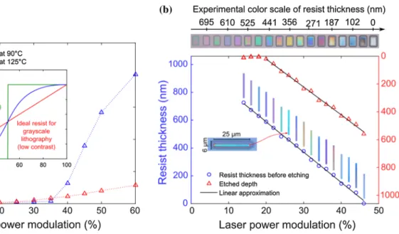
optimized to have a binary comportment, with a high con-trast. This means that under a threshold of exposure dose, the resist development rate tends to zero and is constant and high above it. On the contrary, to perform GL, it is interesting to use a photoresist with low contrast and low selectivity. The ideal case for GL is to have a linear relationship between the exposure dose and the resist development rate (MicroChemi-cals GmbH 2013). To this end, the soft bake process of the AZ ECI 3012 is optimized with respect to standard condi-tions (95 °C, 2 min), by setting its temperature to 125 °C during 5 min. This reinforced thermal treatment decomposes a significant part of the photoactive compounds, which slow-ers and smoothens the relationship between development rate and exposure dose (Fig. 2a). This provides a good con-trol of the removed resist thickness. In addition, development rate becomes independent of development time, contributing to reproducibility and robustness of the process.
After exposure and development, 2.5D structures are patterned in the resist (blue circles in Fig. 2b, remaining resist thickness). Then, they are transferred into silicon by reactive ion etching (RIE). The remaining resist acts as a retardant to start the silicon etching. The two key param-eters of this step are the silicon etching rate, vSi,e, and
the resist etching rate, vr,e. Their ratio defines the etching
selectivity: S = vSi,e∕vr,e. Knowing these etching rates, the
remaining resist thickness, er, and the etching time, te, the
etched silicon depth can be written as: dSi= vSi,ete− Ser.
As illustrated in Fig. 1a, a value of S lower than one reduces the resist thickness variation transferred in silicon, whereas a value higher than 1 increases it. Usually in binary lithog-raphy, RIE is designed to have the highest S as possible. It permits etching a high depth of silicon with a thin layer of resist to achieve a good lateral resolution. Here, the process is optimized to have selectivity around 1: In this way, the resist structures are identically reported in silicon. We also demonstrate tuning of selectivity by playing with etching parameters. This is discussed in SI 2b.
Before designing complex 2.5D structures, 30 µm × 20 µm and straight channels with constant but dif-ferent depths demonstrate the mastery of the process. The only control parameter is the laser power modulation to change the exposure dose (writing velocity v = 0.4 mm/s,
T = 0.3%, and development time 30 s). Figure 2b shows that laser power modulation (m) linearly controls the remain-ing resist thickness before etchremain-ing (in blue), as well as the silicon etched depth for fixed etching conditions (in red). Nanochannels with constant, chosen depths in the range 0–600 nm are thus obtained. The remaining resist thickness can be quickly checked with optical observation; white light interference creates an experimental Newton color scale. The resolution of this measurement is better than 40 nm; that is why it was used for decades in different contexts (Lin and Sullivan 1972). This is very useful for large-scale and
quick characterization of devices. For example, an inten-tional defect is circled in green in Fig. 3 to illustrate that defects can be rapidly identified by color inspection.
In order to get a functional device, the integration of non-uniform-depth nanochannels in the nanofluidic chips is done with standard methods (Fig. 1b). Microchannels of 300 × 5 µm2 cross section are etched by RIE after binary
photolithography in order to supply fluid to the nanochan-nels. Then access holes are sand-blasted in silicon. The chip is capped with a glass wafer by anodic bonding. Before the bonding, a 50-nm thick layer of silicon oxide is thermally grown homogeneously on the silicon surface. It provides a symmetrical wetting condition in channels increasing the hydrophilicity of silicon. It also prevents nanochannel’s collapse, by reducing the electrostatic forces during the bonding (Shih 2004; Duan and Majumdar 2010).
In order to summarize the ability of our process, two different structures are presented in Fig. 3 of GLDWL: slope channels and step channels. In other words, it is feasible to design in one step channels with continuous varying depth, or channels with a depth varying by step. These, 2.5D structures can be seen as elementary com-ponents to design more complex geometries as model to porous media. A feature of our technique is that the Gauss-ian intensity profile of the beam is transferred to the resist, creating non-sharp lateral frontiers. This effect is impor-tant only on a distance of the order of the beam diameter
D. Nanochannels with lateral dimensions no larger than a
few D have a crosssection shape closer to a parabola than to a rectangle. The lateral cross section of channels shown in Fig. 3 is parabolic and varies between 6 µm × 250 nm and 8.1 µm × 400 nm. Larger structures are much less
Fig. 2 a Optimization of the soft bake step to obtain a linear
rela-tion between the development rate and the exposure dose with a low development rate. Process parameters: P0 = 100 mW, T = 3%,
D = 2 µm, v = 5 mm/s. In the inset, ideal comportment of grayscale
or standard photoresist. b On the top: optical image of 20 × 30 µm2
rectangles after resist development, showing Newton color scale.
Main graph: resist thickness after 30 s of development (blue circle, left axis) and depth after 2 min of etching (red triangle, right axis) against laser power modulation of 6 × 25 µm2 rectangles (color figure
online)
Fig. 3 Picture of two slope channels (top) and two channels
com-posed of three steps (bottom), shown in true colors before etching.
Black scale bar is 50 µm. The green circle highlights an intentional
defect. b AFM picture of a step corresponding to the red
rectangu-lar zone in a. The color scale represents a depth from 0 (white) to
affected: 20 × 30 µm2 rectangles on the top of Fig. 2b have
a flat and homogeneous surface.
In terms of writing time, a 400-µm-long straight channel presented in Fig. 3 is written in less than 1 min (a transver-sal line of the stair channel is written in only 0.025 s); The pore network presented in Fig. 4 is written in around 9 min.
The range of achievable depths is 0 to 1 µm with a con-trol over depth better than 10 nm (see standard deviation in Fig. 2b). The lateral minimum width can be reduced down to 2 µm using only 1 beam passage. Large structures can also be designed using adjacent beam passages or a larger beam, which decreases the writing time. The rapidity of the process, its spatial resolution and its versatility to design all kind of complex 2.5 nanostructures are well suited for the prototype phase and application in nanofluidics. In the fol-lowing, we demonstrate the use of our device for fluid flow experiments in complex geometries mimicking a nanopo-rous medium.
3 Quasi‑static drainage
3.1 Experimental nanoslit networks
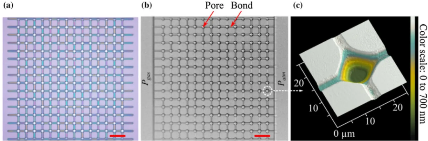
Nanostructures with non-uniform depths fabricated as reported in the previous sections are used to perform drain-age experiments. As illustrated in Fig. 4, a 400 μm × 400 μm quasi-two-dimensional square network is used. It is com-posed of 14 × 16 pores interconnected by 15 × 15 bonds (a bond is the nanoslit connecting two neighbor pores). The depth of a bond is constant all along its length. The depth of each bond is assigned by randomly drawing a depth from six values (in practice, we assign a laser power value which will give a resin thickness developed after lithography and then a depth to the channel as a result of the silicon etching). We
limit ourselves to six values of depth in order to facilitate the control of the robustness of the manufacturing protocol (we can quickly check that two bonds that we want to be of identical depth are indeed of identical depth). The depth of all the pores is the same and is greater than that of the deep-est bond. This is obtained by strong laser exposure of pores. Five devices have been developed (Naillon 2016). Each device has been used several times injecting the displacing fluid on the left side of network and vice versa (so as to obtain two liquid–gas distributions for each device). The repeat-ability was excellent. Basically, the same pattern is obtained when the experiment is repeated with the same device for the same experimental conditions. Also, the experimental result main features are similar for all tested devices and selected injection side. Since similar results are obtained with the five devices, we only present the results obtained with the device corresponding to the slit depths in the smaller range, namely varying between 0 and 225 nm as indicated in Table 1. As can be seen, two depth ranges are indicated in Table 1, one for the vertical bonds and one for the horizontal bonds. Indeed, the slit depth range of this device is slightly shifted between the vertical slits and the horizontal slits due to a technologi-cal choice. For full wafer processing, we slightly defocused the laser beam which writes the structures in order to spread its power over a larger surface. It smoothens uneven etching
Fig. 4 Illustration of network with nanoslits of variable depth. a
Image acquired before etching, after laser lithography and develop-ment. Each color corresponds to a different photoresist thickness
(true colors). b The same device once finished (after silicon etching and bonding to glass). The length scale (red bar) represents 50 μm. c AFM picture around the pore circled in b (color figure online)
Table 1 Experimental nanoslit network geometrical properties: h
denotes the horizontal bonds, and v, the vertical ones (in the image shown in Fig. 4)
Bond depth (nm) h: 30–69–108–147–186–225 v: 0–0–22–61–100–140 Capillary pressure range (bar) h: 6.5–48.5
and exposure that would result from non-horizontality and non-planarity of the substrate. Lateral resolution is still of the order 2 µm as demonstrated in Fig. 4. This defocusing is actually asymmetrical and makes the beam oval rather than circular. The dose of light energy that a point receives then depends on the writing direction, vertical or horizontal. When we indicate a lower bound of depth 0, there is still a thin layer of resist on the silicon at these locations even after etching corresponding to low laser exposure.
3.2 Experimental setup
The drainage experiments are realized on an inverted microscope (Zeiss Axio Observer D1), using a wide-field sensitive camera Andor Zyla sCMos (frequency of acquisi-tion on the order of 1 frame per second). A specific chip holder as well as a pressurization system has been devel-oped owing to the high gas pressures (several tens of bars) required for the drainage experiment (details are presented in SI). The developed high-pressure gas supply line con-sists in connecting a bottle of gas pressurized with 200 bars to the chip holder. The fluid line includes a purge valve to rapidly decrease the pressure, a 3-nm filter and an in-house adapter for connecting the 1/4″ BSP tubing (international standard for gas tubing) to microfluidic material. The line is connected to the bottle via a high-pressure stainless steel flexible tube. A pressure sensor (SETRA brand, Model 2016 / C216) is placed on the line downstream of the filter. The measurements are transmitted via an acquisition card (DAQ, National Instruments) and the reading and recording of the data are made under a LabView interface.
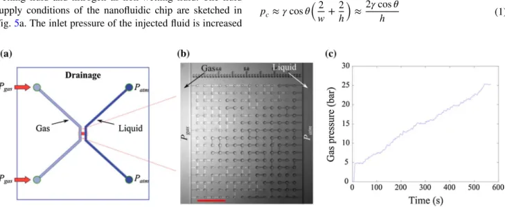
Experiments are carried out using deionized water as wetting fluid and nitrogen as non-wetting fluid. The fluid supply conditions of the nanofluidic chip are sketched in Fig. 5a. The inlet pressure of the injected fluid is increased
step by step, by acting directly on the pressure regulator. Each step corresponds to an increase in pressure between 0.2 and 0.5 bar. We wait for the liquid and gas distribution in the device to be stabilized before increasing the gas pres-sure level again. The value is meapres-sured using the prespres-sure sensor. The experiment is stopped once the breakthrough is reached, that is, when the injected gas exits at the network outlet. The variation of gas pressure applied in the experi-ment is depicted in Fig. 5c.
In order to analyze the experiments and perform their comparison with the numerical simulation, the drainage patterns are extracted by image processing using a code developed with MATLAB ©, described in “Appendix”.
3.3 Numerical simulations
A test to analyze whether the drainage pattern is in agree-ment with Lenormand’s diagram is to compare with a numerical simulation based on the classical invasion per-colation algorithm (Wilkinson and Willemsen 1983). It is well established that this algorithm is adapted for describing the asymptotic regime dominated by capillarity, namely the capillary fingering regime. This algorithm can be summa-rized as follows. The network is invaded step by step start-ing from the inlet. Each step corresponds to the invasion of a single interfacial bond, namely a bond located at the interface between the two fluid phases. The pore occupied by the defending phase and adjacent to the invaded bond is also invaded. The interfacial bond invaded in a given step is the one having the lowest capillary pressure threshold along the gas–liquid interface. Using Laplace’s law, the capillary pressure threshold of a bond is estimated as
(1) pc≈ 𝛾 cos 𝜃(2 w+ 2 h ) ≈ 2𝛾 cos 𝜃 h
Fig. 5 Illustration of drainage experiments in the nanofluidic system: a The experiments are carried out by applying a gas pressure in one
of the supply channels while maintaining the second one to atmos-pheric pressure Patm; b Visualization of a drainage pattern during the
experiment (gas phase in light gray, liquid phase in dark gray). The length scale (red bar) represents 100 μm. c Step-by-step pressure variation in the invading gas phase imposed in the experiment (color figure online)
where γ is the surface tension, θ is the contact angle, h is the slit depth and w is the slit width. Thus, the deeper the slit is, the lower its capillary pressure is. This simple inva-sion rule is combined with the trapping rule stating that a bond must be connected to the outlet through a path occu-pied by the defending fluid. Thus, the interfacial bonds of a trapped liquid cluster cannot be invaded. It is worth not-ing that the simulation is performed with a network havnot-ing the same geometrical properties as the experimental one. In particular, the width and depth of each slit in the numeri-cal network is the same as the corresponding slit in the experimental network (within the experimental accuracy margin of the fabrication process). Since the slit depth can take only six values in each direction, it can happen that several interfacial bonds can be invaded based on Eq. (1). When this is happening, one of those bonds is selected ran-domly. This can affect the order in which various regions of the network are invaded, but tests have shown this has only a little impact on the final pattern (pattern at break-through). In order to perform a comparison with the pres-sure imposed in the experiment, an equivalent drainage pressure Pdrai is associated with each numerical pattern. It
is defined by,
where index i refers to the n bonds forming the invading phase cluster. Thus, Pdrai is actually given by the capillary
(2)
Pdrai= max(pci, i= 1, n) + Patm
pressure threshold of the narrowest bond belonging to the gas cluster (to which the atmospheric pressure is added to obtain the gas pressure).
3.4 Results and discussion
A sequence of experimental binary images and a similar sequence obtained from simulation are presented in Fig. 6. As can be seen, the similarity between the experimental and numerical sequences is strong. It can also be observed that breakthrough at the network outlet takes place at a slightly different position in the simulation compared to the experiment. This can be explained by a slight difference between the experiment and the simulation concerning the size of the slits located in the breakthrough point area. This also explains the somewhat different breakthrough pres-sure observed in the experiment (PBT ~ 20 bars) and the one obtained in the simulation (PBT ~ 15 bars). However,
the simulations for the other fabricated devices (not shown here) lead to the same breakthrough point as in the corre-sponding experiments.
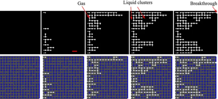
The gas cluster forms a fingering structure. Isolated liquid clusters of various sizes can be also observed. The patterns strongly resemble the classical capillary fingering pattern of Lenormand’s diagram. In our case, the viscosity ratio M is large, of the order of 102, because the viscosity of
the gas is lower than that of the liquid. On the other hand,
Fig. 6 Top drainage sequence in the experiment (gas phase in white,
liquid phase in black). Two liquid clusters are indicated by arrows but several others, composed of one or two bonds, are present in the
images. Bottom a similar sequence obtained from numerical simula-tions (color figure online)
the capillary number, Ca, is difficult to estimate simply because the invasion is driven by pressure step increment and not by imposing an injection flow rate. It tends to zero at the end of the displacement since we wait for the stabi-lization of the two phases between two pressure steps. The velocity of the fluids is therefore zero at the end of each pressure step.
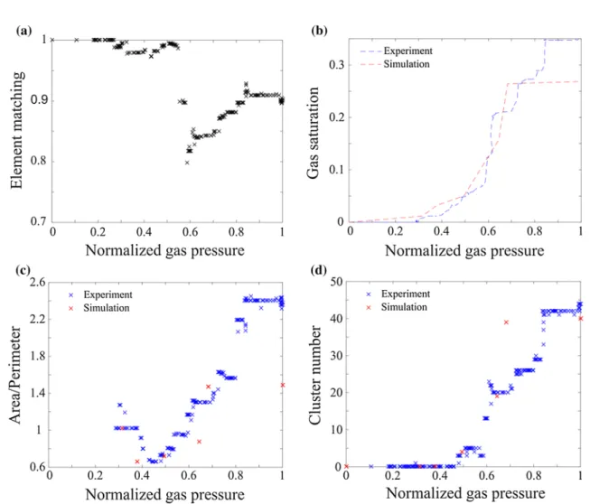
A more quantitative comparison between the experiment and the simulation is presented in Fig. 7. The degree of similarity between the numerical and experimental patterns is first quantitatively determined using an indicator called the element matching indicator. To construct this indicator, the state (liquid or gas) of the same element (pore or bond) in the simulation and the experiment is compared for the same drainage pressure. The element matching indicator between two patterns can be expressed as
(3) EMI= 1 N N ∑ i=1 Ii
where N is the number of elements in the network (N = number of pores + number of bonds); Ii is the
match-ing indicator of element i : Ii = 1 when the considered
element is occupied by the same phase in both patterns, whereas Ii = 0 when this is not the case (liquid in pattern
1 and gas in pattern 2 or vice versa). Thus, EM1 = 1 when the two patterns are perfectly identical, whereas EMI = 0 when no element is occupied by the same fluid in both pat-terns. The closer EMI to 1 is, the greater the degree of sim-ilarity between the two patterns is.
EMI is plotted as a function of the pressure normalized by the experimental breakthrough pressure in Fig. 7a. As can be seen, indicator EMI is about 0.9 at the end of drain-age. This indicates a fairly good agreement between the experimental and numerical drainage patterns. The value of the total indicator decreases to a minimum value of about 0.8 during drainage. This value is explained by a slight offset of the drainage pressure for some elements between the simulation and the experiment, meaning that some
Fig. 7 Comparison between experiment and simulation. The pressure is normalized by the breakthrough pressure PBT (PBT ~ 20 bars in the
elements are drained in the simulation for a lower pressure level than in the experiment.
As discussed, for instance, in Mecke (1996), various other indicators can be defined to quantitatively compare patterns. Figure 7b shows the gas saturation (ratio of the element numbers occupied by the gas phase to the total element numbers in the network), whereas Fig. 7c shows the variation of the ratio of the gas area to its perimeter. The latter corresponds to the exterior perimeter of the invasion pattern and the former is defined as the area of the surface delimited by the exterior perimeter. This indi-cator is related to the global shape of the meniscus (a flat, isotropic drainage leads to a high area/perimeter value, whereas fingers have a large perimeter englobing a low area). Finally, Fig. 7d shows the number of liquid clusters in the system as a function of normalized gas pressure. As can be seen, the agreement between the experimental and numerical patterns is quite good for all considered indicators. However, it can be observed that more isolated clusters forms in the numerical computation compared to the experiment when the normalized gas pressure is around 0.7. Moreover, there are as many clusters at the end, whereas the gas saturation is lower in computation. That means the density of isolated clusters is higher in the computation. This is because the invasion of the pores takes place sequentially in the simulation, one after the other. In the experiment, several pores can be drained at the same time. This is an indication that the experiment does not fully correspond to a pure capillary fingering regime. This reduces the probability of isolated cluster formation. Moreover, it is known that the slit shape (width much larger than depth) favors the formation of thick liq-uid film along the lateral edges of the slits invaded by the gas phase when the top and bottom walls are not perfectly parallel (Geoffroy et al. 2006; Keita et al. 2016). Those films interconnect the different slits and pores together, offering liquid paths for the “isolated” liquid clusters to be drained in the experiments.
The conclusion is therefore that the slow drainage pro-cess in the nanofluidic network with bond depths varying between 0 and 225 nm is not markedly different from the process observed and analyzed in previous works in model systems with much larger bond sizes. Also, the good agree-ment between the experiagree-ment and the simulation indicates that the dominant drainage mechanisms at the pore scale are piston-like motions and Haines jump since they are the mechanisms taken into account in the invasion percola-tion algorithm, albeit rather approximately as regards the Haines jump. As mentioned above, thick liquid films are present in the slits invaded by the gas phase, but the pres-ence of corner films is also classical in systems with pores of greater size (Blunt et al. 2002).
4 Conclusion
We presented a grayscale laser direct writing lithography (GLDWL) method to design structures in 2.5 dimensions in positive photoresist with nanometer depth resolution. We achieved the fabrication of a network of intercon-nected slits with depths in the range 0–225 nm. Lateral resolution depends directly on the laser beam diameter and is around 2 µm in this study. Etching is optimized to reach selectivity around 1 in order to transfer the resist structure into silicon without geometrical distortion. A visual control of the remaining resist thickness based on white light interference enables checking the result of the lithography in a large area at a glance. This technique can be easily incorporated in a standard process flowchart. This study is done optimizing the bake process of a posi-tive photoresist initially developed for binary lithography to adapt it to GL. GLDWL presents the versatility of a maskless technique which is convenient for the prototyp-ing phase. But at the same time, it does not necessitate the very long writing time of other direct writing meth-ods with nanometer resolution as e-beam. In case of large structures, it is also feasible to save writing time with a larger beam diameter. This technique suits very well the needs of nanofluidics: nanometric complex depth profiles (in order to control confinement) and micrometer lat-eral dimension (to have a high throughput in lab-on-chip application, and to work under an optical microscope). This is of high relevance for two-phase flows in nanopo-rous media, since depth controls capillary pressure that in turn controls flow properties. Thus, GLDWL opens the way to further study on nanoconfined fluid, liquid under tension or two-phase flow phenomena. More generally, nanofluidic complex topologies accessible with a simple process have great potential in lab-on-chips, to implement functions such as DNA concentration (Ranchon et al. 2016), or fluidic diodes (Vlassiouk and Siwy 2007). The approach can also be easily adapted to other application fields (optics, MEMS).
The development of GLDWL nanofluidic devices was primarily motivated by the analysis of immiscible two-phase flow in nanoporous materials, an important class of porous media. The aim was to assess whether the drainage process in nanoporous systems is significantly different from what is known in micrometric systems. Our results indicate that the slow drainage process in nanoporous sys-tems well corresponds to the capillary fingering regime in Lenormand’s diagram, and thus can be analyzed within the framework of invasion percolation theory, quite similarly as in micrometric systems. However, it would be worth-while to pursue the study for higher capillary numbers, so to verify the whole Lenormand’s diagram. This would
necessitate developing another fluid delivering system to maintain a constant gas flow at high pressure. The fact that the drainage process is not fundamentally different in our nanofluidic device does not mean this also holds for other two-phase flow processes, such as evaporation and imbibi-tion since, as menimbibi-tioned in the introducimbibi-tion, previous works indicate differences with the behaviors in the micrometric systems.
The situation could also be different in systems involving still smaller pores on the order of 1 nm or less where the clas-sical continuum laws cease to be good approximations (Falk et al. 2015). Also, local deformation was negligible in our experiment. Owing to the high capillary pressures induced by the submicronic sizes, coupling between flow and deforma-tion of the pore space are more likely to occur in nanoporous systems than in micrometric systems (for similar mechani-cal properties of the solid matrix). This can have a great impact on the drainage patterns when the deformability of the medium is sufficiently high, (Holtzman and Juanes 2010).
Acknowledgements This work was partly supported by
LAAS-CNRS micro- and nanotechnologies platform member of the French RENATECH network. It was also supported by LEAF Equipex project. Authors thank also Andra, INSIS-CNRS institute and NEEDS-MIPOR CNRS program for the financial support. We acknowledge P. Dubreuil and A. Lecestre for help with the etching parameters, B. Reig for AFM imaging and J. Prautzsch for help in the pore network simulations.
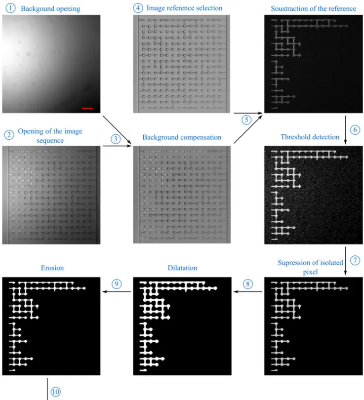
Appendix: Drainage pattern image processing In order to analyze the experiments and perform the com-parison between the experiment and the numerical simu-lation, the drainage patterns are extracted by image pro-cessing using a code developed with MATLAB ©. The purpose of this code is to determine the drained pores and bonds. The various processing steps can be summa-rized as follows and illustrated in Fig. 8 (one can refer to Naillon (2016) for more details). A background image is opened in step 1. It compensates for defects in the homo-geneity of illumination and eliminates dust that may be present on the lens or sensor of the camera. From this image a matrix E is created, which measures the difference in gray level (luminous intensity) between a pixel and the average value of the gray level in the image. Step 2 cor-responds to the opening of the sequence of images using the LibTiff library of MATLAB ©. This library provides functions that are optimized to reduce the opening time of an image stack in .tif format (image sequence into a sin-gle file). The matrix E is subtracted from all the images in step 3 in order to correct the illumination defects. Then, a reference image is extracted from the image sequence in
step 4. It corresponds to the mean value of all the images before the drainage begins (typically the average of more than a dozen images). In step 5, the reference image is sub-tracted from all images. In devices with variable depths, the passage of gas can indifferently increase or decrease the gray level of a channel along its depth. We therefore calculate the absolute value of the difference. We then get an image on which black areas correspond to areas where nothing has happened, and clear areas to areas where there has been a change. The next step is to convert the gray-scale image from step 5 to binary image. This leads to a black and white image that clearly distinguishes where a change has occurred (gas invasion) from where there has been no change. The threshold is first detected automati-cally on an image with the threshold function based on the Otsu method. The latter allows minimizing the inter-class variance of the white and black pixels. The black and white image is obtained in step 6. The program is intended to be interactive and the user can manually mod-ify the threshold after observing the result. In general, a threshold lower than the one proposed automatically by MATLAB is chosen manually even if this leads to a lot of background noises. The objective is to avoid not taking into account drained areas. The image is cleaned in step 7 by eliminating all pixel clusters composed of a number of pixels smaller than a number chosen by the user. Typically, a threshold of 200 pixels (which corresponds to a surface area of about 4.5 × 4.5 μm2) is sufficient to remove the
isolated clusters without removing drained areas. Finally, the dilation and erosion functions are used to eliminate the “holes” of black pixels in the middle of the drained zones. In particular, we realized that the conversion pro-cess in black and white image had difficulty detecting the gray-level variations at the center of the pores. In the same way as for step 6, the user can modify the parameters of steps 7 to 9 interactively by directly controlling the result. The parameters that were used for steps 6 and 9 are then used to process the entire image sequence in the same manner. The last step (10) consists in detecting the state of each pore and bond, drained or not. To this end, we take the median value of the pixels of a window placed in the middle of each pore and bond. If the median value in this window is equal to 1 (white pixel), we consider the pore or the bond as drained. If it is 0, we consider that it has not been drained. For some acquisitions, we observed that some images had a higher average luminous intensity. We think that this phenomenon comes from a poor control of the exposure time of the camera that we had set as low as possible (10 ms). In this case, we added an additional step between steps 3 and 4 to compensate for temporal varia-tions in mean gray levels of the images.
Fig. 8 Illustration of drainage pattern image processing extraction
algorithm. Each image is represented with their full scale of gray level to facilitate observation. To this end, the contrast is increased to get a representation between white and black on all images. The
change in contrast is therefore different from one image to another. For example, for the background image, this representation may wrongly suggest that the inhomogeneity in illumination is quite large. The length scale (red bar) represents 50 μm (color figure online)
References
Azimi S, Dang Z, Zhang C et al (2014) Buried centimeter-long micro- and nanochannel arrays in porous silicon and glass. Lab Chip 14:2081–2089. doi:10.1039/c4lc00062e
Blunt MJ, Jackson MD, Piri M, Valvatne PH (2002) Detailed phys-ics, predictive capabilities and macroscopic consequences for pore-network models of multiphase flow. Adv Water Resour 25:1069–1089
Chauvet F, Geoffroy S, Hamoumi A et al (2012) Roles of gas in capillary filling of nanoslits. Soft Matter 8:10738–10749. doi:10.1039/c2sm25982f
Cottin C, Bodiguel H, Colin A (2010) Drainage in two-dimensional porous media: From capillary fingering to viscous flow. Phys Rev E Stat Nonlinear, Soft Matter Phys 82:1–10. doi:10.1103/ PhysRevE.82.046315
Duan C, Majumdar A (2010) Anomalous ion transport in 2-nm hydro-philic nanochannels. Nat Nanotechnol 5:848–852. doi:10.1038/ nnano.2010.233
Duan C, Karnik R, Lu M-C, Majumdar A (2012) Evaporation-induced cavitation in nanofluidic channels. Proc Natl Acad Sci USA 109:3688–3693. doi:10.1073/pnas.1014075109
Duan C, Wang W, Xie Q (2013) Review article: fabrication of nanoflu-idic devices. Biomicroflunanoflu-idics 7:26501. doi:10.1063/1.4794973
Dullien FAL (1992) Porous media, fuid transport and pore structure. AcademicPress, SanDiego
Erdmanis M, Tittonen I (2014) Focused ion beam high resolution grayscale lithography for silicon-based nanostructures. Appl Phys Lett. doi:10.1063/14866586
Falk K, Coasne B, Pellenq R et al (2015) Subcontinuum mass trans-port of condensed hydrocarbons in nanoporous media. Nat Com-mun 6:6949. doi:10.1038/ncomms7949
Gale MT, Rossi M, Pedersen J, Schulz H (1994) Fabrication of con-tinuous-relief micro-optical elements by direct laser writing in photoresists. Opt Eng 33:3556–3566
Geoffroy S, Plouraboué F, Prat M, Amyot O (2006) Quasi-static liquid-air drainage in narrow channels with variations in the gap. J Colloid Interface Sci 294:165–175. doi:10.1016/j. jcis.2005.07.008
He K, Xu L, Gao Y et al (2015) Evaluation of surfactant performance in fracturing fluids for enhanced well productivity in unconven-tional reservoirs using Rock-on-a-Chip approach. J Pet Sci Eng 135:531–541. doi:10.1016/j.petrol.2015.10.008
Holtzman R, Juanes R (2010) Crossover from fingering to fractur-ing in deformable disordered media. Phys Rev E 82:046305. doi:10.1103/PhysRevE.82.046305
Jung M, Brinkmann M, Seemann R et al (2016) Wettability con-trols slow immiscible displacement through local interfa-cial instabilities. Phys Rev Fluids 074202:1–19. doi:10.1103/ PhysRevFluids.1.074202
Ke K, Hasselbrink EF, Hunt AJ (2005) Rapidly prototyped three-dimensional nanofluidic channel networks in glass substrates. Anal Chem 77:5083–5088. doi:10.1021/ac0505167
Keita E, Koehler SA, Faure P et al (2016) Drying kinetics driven by the shape of the air/water interface in a capillary channel. Eur Phys J E 39:23. doi:10.1140/epje/i2016-16023-8
Kim J, Joy D-C, Lee S-Y (2007) Controlling resist thickness and etch depth for fabrication of 3D structures in electron-beam grayscale lithography. Microelectron Eng 84:2859–2864. doi:10.1016/j. mee.2007.02.015
Lee H, Lee SG, Doyle PS (2015) Photopatterned oil-reservoir micro-models with tailored wetting properties. R Soc Chem 15:3047– 3055. doi:10.1039/c5lc00277j
Lenormand P, Touboul E, Zarcone C (1988) Numerical models and experiments on immiscible displacements in porous media. J Fluid Mech 189:165–187
Li L, Gattass RR, Gershgoren E et al (2009) Achieving l/20 resolution by one color initiation and deactivation of polymerization. Sci-ence 324:910–913
Liao Y, Cheng Y, Liu C et al (2013) Direct laser writing of sub-50 nm nanofluidic channels buried in glass for three-dimensional micro-nanofluidic integration. Lab Chip 13:1626–1631. doi:10.1039/ c3lc41171k
Lin C, Sullivan RF (1972) An application of white light interferom-etry in thin film measurements. IBM J Res Dev 16:269–276. doi:10.1147/rd.163.0269
Madou MJ (2011) Fundamentals of microfabrication and nanotech-nology, vol 3. CRC Press, Boca Raton
Mecke K (1996) Morphological characterization of patterns in reac-tion-diffusion systems. Phys Rev E 53:4794–4800. doi:10.1103/ PhysRevE.53.4794
MicroChemicals GmbH (2013) Greyscale lithography with photore-sists. http://www.microchemicals.com/technical_information/ greyscale_lithography.pdf. Revised 07 Nov 2013
Naillon A (2016) Ecoulements liquide-gaz, évaporation, cristalli-sation dans les milieux poreux et nanoporeux. Etudes à partir de systèmes micro et nanofluidique. University of Toulouse, Toulouse
Prat M (2002) Recent advances in pore-scale models for dry-ing of porous media. Chem Eng J 86:153–164. doi:10.1016/ S1385-8947(01)00283-2
Rammohan A, Dwivedi PK, Martinez-Duarte R et al (2011) One-step maskless grayscale lithography for the fabrication of 3-dimen-sional structures in SU-8. Sens Actuators B Chem 153:125–134. doi:10.1016/j.snb.2010.10.021
Ranchon H, Malbec R, Picot V et al (2016) DNA separation and enrichment using electro-hydrodynamic bidirectional flows in viscoelastic liquids. Lab Chip 16:1243–1253. doi:10.1039/ C5LC01465D
Selimis A, Mironov V, Farsari M (2015) Microelectronic engineer-ing direct laser writengineer-ing : principles and materials for scaffold 3D printing. Microelectron Eng 132:83–89. doi:10.1016/j. mee.2014.10.001
Shih W-P (2004) Collapse of microchannels during anodic bonding: theory and experiments. J Appl Phys 95:2800. doi:10.1063/1.1644898
Stavis SM, Strychalski EA, Gaitan M (2009) Nanofluidic structures with complex three-dimensional surfaces. Nanotechnology 20:165302. doi:10.1088/0957-4484/20/16/165302
Stavis SM, Geist J, Gaitan M (2010) Separation and metrology of nanoparticles by nanofluidic size exclusion. Lab Chip 10:2618– 2621. doi:10.1039/c0lc00029a
Stavis SM, Geist J, Gaitan M et al (2012) DNA molecules descending a nanofluidic staircase by entropophoresis. Lab Chip 12:1174– 1182. doi:10.1039/c2lc21152a
Sugioka K, Cheng Y (2014) Femtosecond laser three-dimen-sional micro- and nanofabrication. Appl Phys Rev 1:041303. doi:10.1063/1.4904320
Totsu K, Fujishiro K, Tanaka S, Esashi M (2006) Fabrication of three-dimensional microstructure using maskless gray-scale lithogra-phy. Sens Actuators A Phys 130–131:387–392. doi:10.1016/j. sna.2005.12.008
Vincent O, Szenicer A, Stroock AD (2016) Capillarity-driven flows at the continuum limit. Soft Matter 12:6656–6661. doi:10.1063/1.2829813
Vlassiouk I, Siwy ZS (2007) Nanofluidic diode. Nano Lett 7:552– 556. doi:10.1021/nl062924b
Washburn EW (1921) The dynamics of capillary flow. Phys Rev 17:273–283
Wilkinson D, Willemsen JF (1983) Invasion percolation: a new form of percolation theory. J Phys A Math Gen 16:3365–3376. doi:10.1088/0305-4470/16/14/028
Witten TA, Sander LM (1981) Diffusion-limited aggregation, a kinetic critical phenomenon. Phys Rev Lett 47:1400–1403 Wu MH, Park C, Whitesides GM (2002) Fabrication of arrays of
microlenses with controlled profiles using gray-scale micro-lens projection photolithography. Langmuir 18:9312–9318. doi:10.1021/la015735b
Wu Q, Bai B, Ma Y et al (2014) Optic imaging of two-phase flow behavior in 1D nanoscale channels. SPE J 19(05):793–802 Zhang C, Oostrom M, Wietsma TW et al (2011) Influence of viscous
and capillary forces on immiscible fluid displacement: pore-scale experimental study in a water-wet micromodel demonstrating
viscous and capillary fingering. Energ Fuels 25:3493–3505. doi:10.1021/ef101732k
Zhang J, Guo C, Zhang H, Liu Q (2013) One-step fabrication of micro/nanotunnels in metal interlayers. Nanoscale 5:8351–8354. doi:10.1039/c3nr01677c
Zhong K, Gao Y, Li F et al (2014) Fabrication of PDMS microlens array by digital maskless grayscale lithography and replica mold-ing technique. Optik (Stuttg) 125:2413–2416. doi:10.1016/j. ijleo.2013.10.082