Spin texture and strain-induced lateral
hetero-structures in GdAg
2
surface alloy
Alexander Correa1,2,3
, Bin Xu4,5,6
, Matthieu J. Verstraete 4,5
, Lucia Vitali1,3,7
1
Departamento de física de materiales, Universidad del País Vasco, 20018 San Sebastián (Spain)
2 Donostia International Physics Center, 20018 San Sebastian (Spain)
3 Centro de Fisica de Materiales (CSIC-UPV/EHU) y Material Physics Center, 20018 San Sebastián (Spain)
4 CESAM and Département de Physique, Université de Liège, B5a Allée du 6 Août 19, B-4000
Sart Tilman, Belgium
5 European Theoretical Spectroscopy Facility (http://www.etsf.eu)
6 Department of Physics and Institute for Nanoscience and Engineering, University of Arkansas,
Fayetteville, Arkansas 72701, USA
7 Ikerbasque Foundation for Science, 48013 Bilbao (Spain)
KEYWORDS (Word Style “BG_Keywords”). Gadolinium hetero-structures, surface strain, electronic and spin texture, scanning tunneling spectroscopy, density functional theory
ABSTRACT
We report on the structural, electronic and magnetic properties of a monolayer of GdAg2, forming a moiré pattern on Ag(111). Combining scanning tunneling microscopy and ab-initio spin-polarized calculations, we show that the electronic band structure can be shifted linearly via thermal dependent strain of the intra-layer atomic distance in a range between 1-7%, leading to lateral hetero-structuring. Furthermore, the coupling of the incommensurable GdAg2 alloy layer to the Ag(111) substrate leads to spatially varying atomic relaxation causing subsurface layer buckling, texturing of the electronic and spin properties, and inhomogeneity of the magnetic anisotropy energy across the layer. These results provide perspectives for a control of magnetic ordering in atomically-thin layers.
Geometrical structure, lattice periodicity and atomic arrangement are subtly intertwined with the electronic properties of materials. Sub-angstrom changes in the atomic distance are sufficient to modify the physical and chemical properties, such as the band-gap, carrier mobility and the chemical reactivity1-14
. The deposition of two-dimensional layered crystals on mechanically stretchable or bendable substrates can produce one-dimensional strained structures with intriguing properties1,2
. Similarly, biaxial-strained two-dimensional layers have been obtained exploiting the interface energy between lattice mismatched epitaxial layers3-9
. The efficiency of these strategies in tuning the electronic properties has generated a considerable progress in tailoring the electronic and optical properties3,8-12
. Few sparse works have demonstrated instead the potentiality of surface-strain in metallic ferromagnetic materials 4-7,12-14
suggesting the applicability of a comparable method to manipulate the magnetic order of strong magnetic materials, which is one of the current challenges for a wide range of applications. Nonetheless, a general picture on the influence of atomistic structure on the local magnetic order is still missing.
Here, we will show that both electronic and magnetic properties of two-dimensional layer critically depend on the local atomic arrangement. Surface strain inherent in epitaxially-grown two-dimensional layers is sufficient to texture the electronic and the magnetic properties of a ferromagnetic structure stable up to 85K 15
. Specifically, we will characterize a monolayer structure based on rare-earth surface stoichiometric alloy GdAg2 forming a weakly interacting moiré superstructure on Ag(111). This monolayer is particularly suitable to investigate the relation between the structural, electronic and magnetic properties. Indeed, in rare-earth based materials, the exchange interaction process and, consequently, the magnetic order are critically
sensible to structural variations and orbital hybridizations 5-7, 12-14
which affects the delicate interplay between the 5d, 6s nearly-free conduction and the highly-localized 4f electrons.
Here, we will demonstrate that in-plane lattice strain conveys to the formation of hetero-structures with variable alloy unit-cell (in the range of 5.15-5.6Å) and distinct density of states. Moreover, the incommensurate alloy layer induces an out-of-plane atomic buckling of the supporting substrate with the periodicity of the moiré structure. This prompts a position dependent coupling interaction to the Ag(111) surface, steers a modulation in the density of states and leads to a local weakening of the ferromagnetic order resulting in a spin-texture across the layer. The direct comparison of scanning tunneling microscopy (STM) and spectroscopy (STS), with state-of-the-art spin-polarized numerical simulations based on density functional theory (DFT), facilitate the understanding of the role of strain, structural relaxation and coupling interaction on the physical-chemical properties of the system.
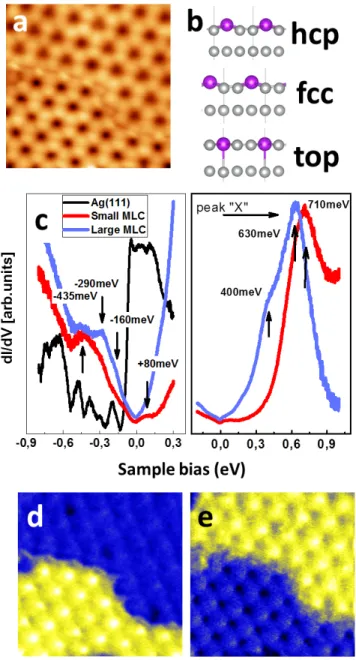
A monolayer of GdAg2 forms an incommensurate structure on Ag(111), similar to the previously reported GdAu2 on the Au(111) surface
15,16 (see Supporting Information S1). This results in topographic STM images (Figure 1a) as a moiré superstructure, whose apparent minima and maxima reflect the variation of the geometrical registry of the atoms of the alloy layer with respect to the Ag(111) surface. Three of the canonical geometrical configurations, namely hcp, fcc and top, through which the atoms of the continuous alloy layer must pass periodically are shown in Figure 1b. Considering each of these stacking configurations separately, we provide a picture of the physical and chemical variation along the alloy layer and at its interface with Ag(111).
Using first-principles calculations17-18(details in Supporting Information S2), we show that the formation of the superstructure induces different relaxations of the supporting substrate according to the stacking registry of the alloy layer. The Gd atoms are found 2.872 Å (2.870 Å) above the substrate in the fcc (hcp) stacking configuration, while for the top configuration the preferred position is slightly lower, i.e. 2.794 Å. Correspondingly, the Ag atoms of the substrate below the Gd atoms are pushed into the bulk of the crystal (Figure 1b). The modeling of these configurations allows us to assign the top stacking to the valleys of the topographic image and the fcc and hcp to the hills (i.e., to the “dark” and “bright” sites), respectively. The clearly distinct relaxation of the system in top stacking has a critical role in the electronic properties and in the local spin order of the alloy, as will be shown here.
A closer analysis of Figure 1a shows that the two neighboring moiré superstructures differ in their relative orientation and periodicity having the upper-right one a large moiré lattice constant (hereafter, LMLC) and the other a smaller one (SMLC). The local density of states, measured using standard lock-in techniques on the hills of the two super-structures, is shown as red and blue lines in Figure 1c. The corresponding dI/dV spectra achieved on the valley positions and space-resolved energy maps are shown in Supporting Information S3-S5 The local spectroscopic data shown in Figure 1 demonstrate clearly that the two superstructures differ both in their occupied as well as the empty states. A characteristic feature at 400meV, visible as a shoulder of a higher energy peak occurring at about 630meV, characterizes the LMLC pattern. This peak (hereafter, labeled “X”) shifts to higher energy (710 meV) as the lattice constant of the moiré pattern is reduced. An unequivocal localization of these states in either of the two moiré areas can be evinced by the conductance maps (Figure 1 c and d), corroborating the formation of
lateral electronic hetero-structures. Further differences between the two superstructures can be observed in the low-energy region, where an additional small peak can be observed at 80meV and in the higher- energy region (see supporting information S3-S4). The occupied density of state equally differs in the two superstructures. Their reduced intensity and many shoulders impede, however, a clear quantification of their energy positions. The overall emerging picture is that a reorganization of the electronic properties takes place as a function of the superstructure lattice size. Notably, the surface state of Ag(111) cannot be further observed through the moiré pattern. This suggests that a modification of the electronic properties of the noble metal surface has occurred despite the formation of moiré patterns is indicative of a weak coupling to the supporting substrate.
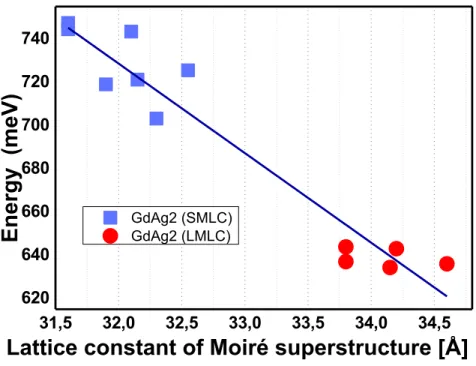
The spectra shown in Figure 1b are representative of a series of dI/dV measurements achieved on different moiré superstructures. A careful data analysis of these shows that the energy position of peak X varies as a function of the lattice constant of the superstructure according to the statistical distribution shown in Figure 2. The observed energy values cluster around two mean values of the superstructure periodicity, 32 and 34Å. The relation between the electronic structure and lattice constant is further corroborated by a fit of the data (blue line in Figure 2), which suggests a linear dependence. This is confirmed by first principle calculations, as it will be shown in the following.
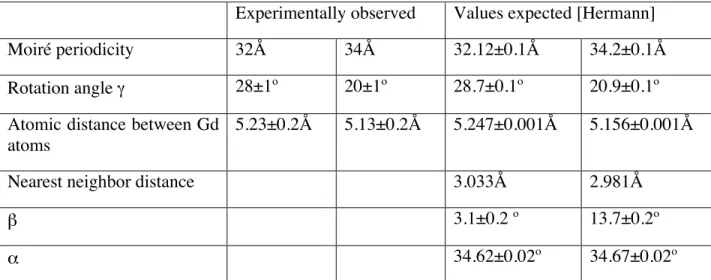
To understand the observed relation between the lattice constant of the superstructure and the resulting electronic properties, we have applied to the system the coincidence model proposed by Hermann to describe moiré patterns20. This model envisions the moiré super-structure as a
coincidence network formed by the atoms of the overlayer that periodically match those of the substrate. Outcomes of the model are the size of the unit cell of the alloy and its angle of rotation α with respect to the Ag(111) high symmetry directions (see Supporting Information S6 for further details). Among the possible moiré patterns predicted by the Hermann model for this system, the structural parameters of two (table 1) allow a direct association to the experimentally observed high-resolution images on the two moiré superstructures (see Supporting Information S3). Experimental results and modeling consistently show that the unit cell size of the alloy monolayer and its orientation differ in the two moiré patterns seen in in Figure 1. The two periodicities of 32 and 34 Å respectively, correspond to alloy unit cells differing in size by a relative strain of 1%, while the angle α is almost constant. The superstructure with larger periodicity, i.e. with the larger coincidence distance, is formed by the alloy layer with the smaller lattice constant, in good agreement with the experimental observations20-22 and intuitive expectations.
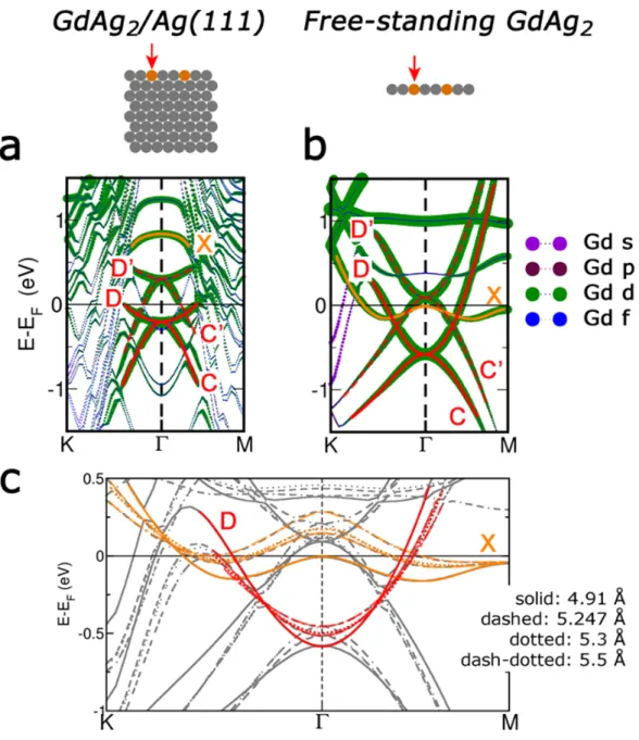
Guided by this understanding of the structural origin of the two moiré patterns, we simulated their electronic properties with density functional theory (see Supporting Information S2). The band structure of the GdAg2 alloy is first calculated with the supporting layer Ag(111) and then compared with the free standing case. In this way, we separate the effect of strain on the alloy from the interaction with the substrate, achieve a base line for the band character, estimate the importance of surface interactions, and of the magnetic anisotropy energy. The electronic structure of the GdAg2/Ag(111) was calculated using a commensurate √3x√3 supercell of the noble metal (111) surface in the plane in fcc stacking, which is the configuration with
lowest-energy (Figure 3a). The hcp and fcc stackings (Supporting Information S2-S6-S7 share most properties, but differ from the top case in the band energy positions and dispersion.
The free-standing GdAg2 alloy layer, calculated using the same parameters as in the supported
case, is shown in Figure 3b. Upon the removal of the supporting substrate few bands shift towards lower energies considerably more than the other bands of the system (C and C´). This is an artifact of the free-standing approximation, which highlights their coupling potential with the Ag(111) surface. The effective coupling potential acting on the surface-supported alloy monolayer is expected to be intermediate between the free standing and the theoretical commensurate case shown in Figure 3a and b, respectively.
The free standing alloy is then progressively strained to survey the impact on the band structure. Relaxed and strained structures are compared in Figure 3b and c. The color code of the lines highlights in both cases the correspondence of the two bands around the Γ point, namely X and D, whose contribution dominates the dI/dV spectra. These have a mixed Gd-d, Ag p and Ag d character and play a critical role in the magnetic character of the system15. Outcome of these calculations is the relative position of the D and X bands as a function of strain, while their absolute energy position is shifted towards negative energies by the approximation used as discussed above. By increasing the size of the alloy unit cell, i.e., decreasing the periodicity of the moiré supercell, the empty states band X shifts towards higher energies (Figure 3c) explaining quite straightforwardly the shift of peak X shown in Figure 1 and 2. A similar effect was observed also in graphene layers and in MoS2 where a linearly increasing gap of about
100meV per strain percentage was reported23-24. The X band presents minima at slightly larger k momentum in the Brillouin zone, which become shallower at larger lattice constants. This and the onset of the C’, D’ bands are tentatively assigned to the shoulder observed at 400meV.
Energy shifts are also predicted for the occupied states (red line). The clearly diminishing intensity at low energy and the appearance of a peak at 80meV with the increased lattice size confirm the predicted trend of an upward shift of the D band. Bearing in mind the shortcomings of the used approximation and the onset of Ag(111) bulk state26-26, not visible in the present calculations, the agreement between experimental and theoretical results can explain quite straightforwardly the main feature of the density of states as a function of lattice structure.
Remarkably, on Au(111) the GdAu2 alloy do not form moiré hetero-structures. This can be explained considering the calculated surface binding energies using Esurf = Ehetero - EML – Eslab, where Ehetero, EML, and Eslab are the total energies of the hetero-structure, the free standing monolayer, and of the 7-layer noble metal substrate, respectively. Whereas, the binding energy of GdAg2 on Ag(111) is in the range 3.10-3.97 eV per unit cell in the three stacking configurations, a considerably higher binding energy (between 9.96-10.48 eV) is found for GdAu2 on Au(111). Such energy limits the spontaneous arrangements and orientation of the GdAu2 alloy layer on the Au surface compared with the case of Ag.
The GdAg2 alloy layer can be strained further by depositing Gd at a slightly lower temperature (240ºC). As shown in Figure 4, at this temperature large portions of the surface are tessellated by hexagonal cells of uniform size, formed by a GdAg2 layer with a lattice constant of 5.5Å. Each hexagonal tile is 5-6 GdAg2 unit cells wide (Figure 4b). At this critical size strain cannot be sustained further and discommensuration lines appear as sketched in Figure 4c. Despite the clear change in the STS density of states measured at the disconmensuration lines (Figure 4d), the spectrum measured on the tile closely resembles the one of the moiré superstructures reported in
Figure 1. The main difference is a further decreased of the low-energy density of occupied states, where the peak at -440meV remain almost unaffected and the lowest unoccupied electronic feature shift further to +270meV. This agrees with the predicted trend of the onset of the D band as a function of lattice periodicity already discussed for the moiré superstructures.
The magnetic character of the GdAg2 alloys can be probed by considering the energies of the plane and out-of-plane magnetic orientations for the three stacking shown in Table 2. The in-plane magnetization is energetically preferred with respect to the out-of-in-plane direction by 168 meV for hcp and fcc stacking. On the contrary, the top stacking configuration has no anisotropy energy and, is energetically much less stable (0.7-0.8eV). An in-plane ferromagnetic character was experimentally observed in magnetic measurements averaging over the moiré superstructure of GdAg2 15. As the continuity of the layer imposes that GdAg2 alloy will be found also in top
position, our calculations suggest the formation of a magnetic texture along the layer, where top positions behave as paramagnetic dots embedded in an otherwise in-plane ferromagnetic layer. Even if the magnetic hardness here described were overestimated by the imposition of commensurate boundary conditions, which increases the atomic orbitals overlap of the alloy and of the Ag(111) substrate, we expect that the trend in the magnetic anisotropy will be preserved.
The calculated magnetic anisotropy energies between in-plane and out-of-plane spin orientation are quite large in fcc and hcp, and would correspond to a Curie temperature of 1950K according to mean field theory. The observed critical temperature of 85K 15 can be understood in terms of in-plane magnetic disorder, where the spin orientation is parallel to the surface but fluctuates between different in-plane orientations. The very low out-of-plane anisotropy in the top
configuration should further weaken the total magnetic state and contribute to reduce the observed Tc. Free standing alloy layers subjected to strain present similar anisotropy energies
(see Table S1 of Supporting Information).
In conclusion, the intimate relation between atomic structure, electronic and magnetic properties allows for controlling through structural relaxation the physical properties of materials and to modulate in space the energy structure and the magnetic order. The comparison between experimental local structural and spectroscopic measurements and theoretical predictions let us surveying two major contributions in the occupied and empty band structure of the incommensurate GdAg2 monolayer grown on Ag(111) as a function of in-plane lattice strain. This is reflected in the electronic structure and leads to surface hetero-structuring. Furthermore, out-of-plane structural relaxation leads to buckling of the atomic structure and variation of the interlayer distance texturing the electronic and magnetic properties of the GdAg2 monolayer with the periodicity of the moiré superstructure. We predict that the magnetic hardness changes across the moiré superstructure leading to a ferromagnetic layer with paramagnetic dots corresponding to the top stacking configuration of the GdAg2 alloy. We believe that the intimate relation found here between structural, electronic and magnetic properties have a general validity in weakly interacting layered systems, most of which form moiré superstructures.
Figure 1. Structure and electronic properties of a monolayer thick GdAg2 on Ag(111). (a) Two GdAg2 moiré
superstructures differing in lattice constants are seen in topographic images. Up: large moiré lattice constant (LMLC); down: small moiré lattice constant (SMLC).Image size 20nm2 (b) Calculated relaxed geometry for the
alloy layer in hcp, fcc and top configuration of one monolayer of GdAg2 on Ag(111). (c) dI/dV spectra acquired on
the two moiré superstructures. (d-e) Conductance maps at 380meV and 700meV, showing the localization of the electronic peaks in only one of the LMLC or the SMLC. All experimental data presented here have been acquired using a low temperature scanning tunneling microscope operated at 77K 19
Figure 2. Correlation between the lattice constant of the moiré pattern and the energy of electronic structure. Energy shifts around equilibrium positions are observed monitoring peak X both in the SMLC (i.e. large
alloy unit cell) and LMLC (i.e. small alloy unit cell) patterns (blue and red symbols). The line is a linear fit of the experimental data points.
31,5 32,0 32,5 33,0 33,5 34,0 34,5 620 640 660 680 700 720 740 GdAg2 (SMLC) GdAg2 (LMLC)
Energy (meV)
Experimentally observed Values expected [Hermann]
Moiré periodicity 32Å 34Å 32.12±0.1Å 34.2±0.1Å
Rotation angle γ 28±1º 20±1º 28.7±0.1º 20.9±0.1º
Atomic distance between Gd atoms
5.23±0.2Å 5.13±0.2Å 5.247±0.001Å 5.156±0.001Å
Nearest neighbor distance 3.033Å 2.981Å
β 3.1±0.2 º 13.7±0.2º
α 34.62±0.02º 34.67±0.02º
Table 1. Comparison between the experimentally observed and the calculated valued of the moiré super-structures
Figure 3. Density functional theory calculations of the band structure of GdAg2: (a) Calculated band structures
of the GdAg2 alloy layer with (√3x√3)R30º periodicity, in fcc configuration on Ag(111) (left panel). Color lines
highlight the band structure responsible for the main observed density of states in Figure 1. (b) Calculated band structure for the free-standing GdAg2 alloy layer with the same lattice constant as the Ag (111) substrate (c)
Calculated band structures of the free standing GdAg2 alloy layer for different lattice constants. The main bands that
Simulated magnetization anisotropy energy
In-plane Out-of-plane
Surface alloy position hcp fcc top hcp fcc top
Energy relative to in-plane fcc (meV)
24 0 852 192 168 852
Table 2. The calculated out-of-plane magnetic anisotropy (Eout-of-plane – Ein-plane) of hcp, fcc and top surface alloy
configurations for GdAg2 alloy with Ag substrate. The energies are in meV per formula unit of alloy, and relative to
the lowest energy configuration. Note that a (much smaller) in-plane anisotropy exists as well: the out-of-plane anisotropy is a signature of the overall strength of the ferromagnetic state.
Figure 4. Hexagonal network of GdAg2 under large strain. (a-b) Topographic images of the alloy layer showing
hexagonal patterns tessellating the Ag(111) surface. (a. 25x25nm, 1eV; b. 13x13nm, -31meV). The alloy unit cell (black) and hexagons (white) are drawn on the figure as guide to the eye. (c) Graphical representation of the hexagonal network. (d) dI/dV spectra taken at different positions moving from the center towards the disconmensutration line.
ASSOCIATED CONTENT
Further details of the sample preparation, data analysis and calculations models in the different stacking configurations can be found in the Supporting Information. http://pubs.acs.org.”
AUTHOR INFORMATION Corresponding Author lucia.vitali@ehu.eus
ACKNOWLEDGMENT
AC and LV acknowledge the financial support of the Spanish ministry of economy (MAT2013-46593-C6-4-P)
MJV and BX acknowledge two ARC grants (TheMoTherm #10/15-03 and AIMED # 15/19-09) from the Communauté Française de Belgique, a PDR project (GA T.1077.15) from the Fonds National pour la Recherche Scientifique (Belgium). Computer time was provided by CECI, SEGI, Zenobe/CENAERO (Walloon region GA 1117545), and PRACE-2IP and 3IP (EU FP7 GA RI-283493 and RI-312763) on EPCC Archer.
REFERENCES
(1) Conley H.J., Wang B., Ziegler J.I., Haglund R. F. Jr., Pantelides S. T., Bolotin K.I.; Bandgap Engineering of Strained Monolayer and Bilayer MoS2; Nano Letters, 2013,13, 3626
(2) Castellanos-Gomez A., Roldan R., Cappelluti E., Buscema M., Guinea F., van der Zant H.S. J., Steele G.A.; Local Strain Engineering in Atomically Thin MoS2; Nano Letters, 2013 13, 5361
(3) Cheng S., Yu J., Ma T., Peres N. M. R. Strain-induced edge magnetism at the zigzag edge of a graphene quantum dot; Physical Review B 2015, 91, 075410
(4) Neuhold G.; Horn K.; Depopulation of the Ag(111) Surface State Assigned to Strain in Epitaxial Films Phys. Rev. Lett. 1997, 78, 1327
(5) Yakovkin I.N., Komesu T.; Dowben P.A.; Band structure of strained Gd(0001) films; Phys. Rev. B 2002, 66, 035406
(6) Waldfried C.; McAvoy T.; Welipitiya D.; Komesu T.; Dowben P.A.; Vescovo E. Wave-vector-dependent exchange splitting in a local moment system; Phys. Rev. B 1998, 58,7434 (7) Andrianov A. VI; Savel’eva O.A., Bauer E.; Staunton J.B.;Squeezing the crystalline lattice
of the heavy rare-earth metals to change their magnetic order: Experiment and ab initio theory; Phys. Rev. B 2011, 84, 132401
(8) Bokdam M., Amlaki T., Brocks G., and. Kelly P.J.; Band gaps in incommensurable graphene on hexagonal boron nitride Phys. Rev. B 2014, 89, 201404R
(9) AmorimB., Cortijo A., de Juan F., Grushin A.G., Guinea F., Gutiérrez-Rubio A., Ochoa H., Parente V., Roldán R., San-Jose P., Schiefele J., Sturla M., Vozmediano M.A.H.; Novel effects of strains in graphene and other two dimensional materials; Physical Report 2016, 617,1;
(10) Fogler M. M., Guinea F., Katsnelson M. I.; Pseudomagnetic Fields and Ballistic Transport in a Suspended Graphene Sheet; Physical Review Letters 2008 101,226804; (11) Klimov N. N., Jung S., Zhu S., Li T., Wright C. A., Solares S. D., Newell
(12) Vescovo, E ; Carbone, C; Rader, O; Surface magnetism of Gd(0001) films – evidence for an unexpected phase transition; Physical Review B 1993, 48, 7731
(13) Mathias Getzlaff M. Surface magnetism; Springler Verlag, 2010 Berlin
(14) Waldfried C., McIlroyy D N , Dowben P A; The electronic structure of gadolinium grown on Mo(112); J. Phys.: Condens. Matter 1997 9 10615
(15) Ormaza M., Fernandez L., Ilyn M., Magaña A., Xu B., Verstraete M. J., Gastaldo M.,Valbuena M. A., Gargiani P., Mugarza A., Ayuela A., Vitali L., Blanco-Rey M., Schiller F., Ortega J. E.; High Temperature Ferromagnetism in a GdAg2 Monolayer Nano
Letters 2016, 16, 4230
(16) Fernandez L., Blanco-Rey M., Ilyn M., Vitali L., Magaña A., Correa A., Ohresser P., Ortega E., Ayuela A., Schiller F.,; Co Nanodot Arrays Grown on a GdAu2 Template: Substrate/Nanodot Antiferromagnetic Coupling Nano Letters 2014, 14, 2977
(17) Gonze X.; A brief introduction to the ABINIT software package Zeitschrift für Krist. 2005, 220, 558
(18) X. Gonze , , B. Amadon, P.-M. Anglade, J.-M. Beuken, F. Bottin, P. Boulanger, F. Bruneval, D. Caliste, R. Caracas, M. Côté,T. Deutsch,L. Genovese,Ph. Ghosez, M.
Giantomassi, S. Goedecker, D.R. Hamann, P. Hermet, F. Jollet, G. Jomard, S. Leroux, M. Mancini, S. Mazevet, M.J.T. Oliveira, G. Onida, Y. Pouillon, T. Rangel, G.-M. Rignanese, D. Sangalli, R. Shaltaf, M. Torrent, M.J. Verstraete, G. Zerah, J.W. Zwanziger;ABINIT: First-principles approach to material and nanosystem properties Comput. Phys. Commun. 2009, 180, 2582
(19) The non-working performances of the TYTO-STM (SPECS) impeded to reach lower temperatures.
(20) Hermann K.; Periodic overlayers and moiré patterns: theoretical studies of geometric properties; J. Phys. 2012, 24, 314210
(21) Vitali,L.; Ramsey,M.G.; Netzer, F.P.;,
Rotational epitaxy of a ‘soft’ metal overlayer on Si(111); Surface Science 2000, 452, L281
(22) Sutter, P.; Sadowski, J.T., Sutter E.; Graphene on Pt(111): Growth and substrate interaction Phys. Rev. B 2009, 80, 245411
(23) Conley H.J,, Wang B., Ziegler J.I., Haglund R.F., Pantelides S.J., Bolotin K.I. Bandgap Engineering of Strained Monolayer and Bilayer MoS Nano lett.13.3626 (2013);
(24) Peelaers H., Van de Walle C. G. Effects of strain on band structure and effective masses in MoS2 Phys. Rev B 2012, 86, 241401(R)
(25) Vitali L., Wahl P., Schneider M.A., Kern K., Silkin V.M., Chulkov E.V., Echenique P.M. Inter- and intraband inelastic scattering of hot surface state electrons at the Ag(111) surface Surface Science 2003, 523, L47
(26) Paniago R., Matzdorf R., Meister G., Goldmann A.; Temperature dependence of Shockley-type surface energy bands on Cu(111), Ag(111) and Au(111) Surface Science 1995 336,113