HAL Id: hal-03039192
https://hal.archives-ouvertes.fr/hal-03039192
Submitted on 3 Dec 2020
HAL is a multi-disciplinary open access
archive for the deposit and dissemination of
sci-entific research documents, whether they are
pub-lished or not. The documents may come from
teaching and research institutions in France or
abroad, or from public or private research centers.
L’archive ouverte pluridisciplinaire HAL, est
destinée au dépôt et à la diffusion de documents
scientifiques de niveau recherche, publiés ou non,
émanant des établissements d’enseignement et de
recherche français ou étrangers, des laboratoires
publics ou privés.
Chalcogenides
Alain Lafond, Catherine Guillot-Deudon, Michaël Paris, Maria Caldes,
Stéphane Jobic
To cite this version:
Alain Lafond, Catherine Guillot-Deudon, Michaël Paris, Maria Caldes, Stéphane Jobic. Crystal
Chemistry Investigations on Photovoltaic Chalcogenides. Cristallography in Materials Science: From
Structure-Property Relationships to Engineering, In press. �hal-03039192�
Alain Lafond, Catherine Guillot-Deudon, Michaël Paris, Maria Teresa Caldes,
Stéphane Jobic
Crystal Chemistry Investigations on Photovoltaic
Chalcogenides
Keywords: Chalcogenides, CZTS, CIGS, Photovoltaic, X-ray crystallography, NMR spectroscopy, Ternary diagram,
Phase stability.
1 Introduction
Photovoltaics (abbreviated PV hereafter) is a generic term to describe the direct conversion of light (very often from the sun) into electricity. Basically, a photovoltaic solar cell is a pn junction (semiconducting materials) in which photons are absorbed and give rise to electron-hole pairs. These carriers are collected on both sides of the cell leading to a photovoltage and a photocurrent in the outside circuit, thus available to operate devices. The market is, by far, still dominated by the silicon-based technology1 although emerging materials are of interest. Among them, copper-based chalcogenides have strong potential applications specifically for thin film solar cells (i.e. low amount of active materials) due to their high light absorption coefficient2 and their band gap tunability3,4.
To date, solar cells based on Cu(In,Ga)Se2 (CIGSe) and CdTe have high energy conversion efficiency5,6. However, some of the chemical elements involved in these materials suffer from either scarcity or toxicity issues. Thus compounds derived from Cu2ZnSnS4 (CZTS) have been proposed as alternative absorbers7. On the other hand, as the efficiency of a solar cell based on a single pn junction is intrinsically limited to about 30% (known as Shockley–Queisser limit8), the concept of tandem solar cell has been proposed9 to overpass this limit. In such devices, more of the solar spectrum can be absorbed; the photons of lowest and highest energy are absorbed in the bottom cell (band gap of about 1.1 eV) and in the top cell (Eg around 1.7 eV), respectively. In this scenario, Cu(In,Ga)S2 (CIGS) compounds receive a strong incentive to be used as absorber in the top cell, the bottom one being based on Si technology.
Whatever, before launching of a new product on the market, fundamental knowledge on the chemical and physical properties of materials have to be amassed. In particular, to optimize opto-electronic properties, the relationship between crystal structure (long and short ranges) and materials properties have to be clarified. In this context, we have thoroughly studied CZTS and CIGS compounds through a crystal chemistry approach. Indeed, the crystal structure is the key venue to rationalize and move forwards. In this chapter, we have selected two specific topics: the study of the cationic disorder in CZTS materials and the investigation of the phase equilibria in the Cu2S - In2S3 - Ga2S3 pseudo-ternary system. Our aim is clearly to highlight the capital importance of X-ray diffraction techniques (especially on single crystals) and Nuclear Magnetic Resonance (NMR) spectroscopy in the in-depth characterization of solid materials.
2 Experimental
In the two thorough crystal chemistry investigations presented here, the use of highly pure and very well character-ized samples is of high importance. Thus the experimental procedures (synthesis and chemical analyses) are key steps and are briefly described hereafter. In addition, few words are given to contextualize the inputs of the single crystal resonant X-ray diffraction and of the solid state NMR spectroscopy.
2.1
Synthesis
The studied compounds in the Cu2S-ZnS-SnS and Cu2S-In2S3-Ga2S3 systems were synthesized by ceramic route which consists of a high temperature reaction between the precursors in evacuated quartz ampoules. Namely, pure ele-ments or binary sulfides are weighted in an appropriate ratio and pressed into pellets (when possible), and introduced in a silica tube. Once sealed under vacuum, the mixture is heated up to 750-900°C for periods ranging from 2-3 days to 1-2 weeks. Afterwards the samples may be homogenized by grinding, pressed into pellets again and annealed at the same
temperature. At this step, samples can be slow cooled or quenched in water. This synthesis route was adapted from the one proposed by Bernardini10 and Schorr11. In a number of cases, iodine is added to favor crystal growth and get crystals large enough (typically 10-20 microns in each dimension) for single crystal X-ray studies.
2.2
Elemental chemical analyses
The Energy Dispersive X-ray (EDX) analyses were done using a scanning electron microscope (JEOL 5800 LV) with an accelerating voltage of 20 kV. As the elemental composition is a crucial point as part of this study particularly, careful analyses were systematically carried out on polished sections of the powders imbedded in epoxy. The elemental percentages were calculated using internal calibration in order to achieve both accurate and precise results. The standards were: Cu metal (Cu-Kα), InAs (In-Lα), GaP (Ga-Kα), ZnS (Zn-Kα), SnO2 (Sn-Lα), FeS2 (S-Kα). Collected EDX data were systematically validated by checking the charge balance equilibrium with Cu+, In3+, Ga3+, Zn2+, Sn4+ and S2- ions. In the case of the CIGS derivatives the stoichiometric compound (Cu1.005(5)In0.483(4)Ga0.512(3)S2.000(9)), well characterized by Powder X-ray diffraction (PXRD) and electron microprobe analysis, was used as a secondary standard.
2.3
Conventional X-ray diffraction in laboratory
Powder X-ray diffraction measurements were carried out a Brucker D8-Advance diffractometer in a Bragg-Brentano geometry using monochromatic radiation Cu(K-L3, λ = 1.540598 Å) and a LynxEye detector. Powder patterns were recorded in the 8-100° 2θ-range, 2θ-step = 0.008°. The full pattern matching and Rietveld analyses were performed thanks to Jana2006 program12.
For the single crystal structure determinations, data collections were done on a Brüker Kappa CCD instrument, using graphite monochromated Mo KL2,3 radiation (0.71073 Å) with the ρ- and ω-scan techniques. The recorded images were processed with the set of programs of Nonius. The structures were refined using also Jana2006 program.
2.4
Single crystal resonant X-ray diffraction
In X-ray diffraction experiments, scattering comes from the interaction of the impinging light with electrons of matter. The power of such scattering by a given atom depends on its atomic scattering factor f which is a complex term,
f = fo + f' + if". The non-resonant factor fo is related to the atomic number of the corresponding atom and is energy
independent but decreases when the scattering angle (sin(θ)/λ) increases. On the contrary, the f' and f" terms, known as the resonant factors, are quite independent of the scattering angle but hugely dependent on the X-ray photon energy near the edge of the scattered atom (see Figure 3.1). In conventional X-ray diffraction experiment, very often the contributions of f' and f" remain very low compared to that of fo. In those conditions neighbor elements in the periodic table have very
close atomic scattering factors and appear to be roughly identical in X-ray diffraction analyses. This situation occurs in CZTS compounds for copper and zinc (identical electronic configurations for Zn2+ and Cu+ cations). Thus, Cu/Zn dis-tribution in the crystal structure of CZTS compounds is hard to address by conventional X-ray diffraction. In contrast, resonant X-ray diffraction (i.e. close to absorption edge of one of the constituent element) is known to enhance the contrast between elements which are close in the periodic table13. This method requires finely tuned photon energy which is readily available at synchrotron facilities. Let us notice that neutron diffraction could also be employed as reported by Schorr14.
Figure 3.1: Calculated f' and f" scattering factors for copper and zinc close to their Kα absorption edges (Dispano software with Sasaki data).
In CZTS compounds, the single crystal X-ray resonant diffraction technique has been used to investigate the copper-zinc distribution (see below). Practically, single crystals were picked up from powders and sorted out via preliminary diffraction data collection at the laboratory to check their quality. The best ones were selected for resonant diffraction investigations on the CRISTAL beamline at the Soleil French synchrotron. In order to increase the contrast between Cu and Zn data, sets were collected just below both the Cu Kα and Zn Kα absorption edges, at λ = 1.3825 (2) Å and λ = 1.2844 (2) Å, respectively. An extra data set was collected far from the absorption edges at λ = 0.66842 (4) Å. All crystal structure refinements were performed using JANA200612 using the anomalous scattering factor values from Sasaki data given by the Dispano program15. More details about these experiments can be found in the original paper16.
2.5
Solid state NMR spectroscopy
The 119Sn spectra were acquired on Bruker Avance III 300 MHz (7 T) spectrometer using a 4 mm CP-MAS probe. This set up appears as a good compromise since the use of low magnetic field avoids the too large spreading of spectra due to chemical shift anisotropy. Moreover, the T1 relaxation time, then the recycle time, which can be quite long for ½ spin nucleus in crystalline compound is lowered. Finally, the large volume of 4 mm rotor allows to reduce the number of scan while keeping a high MAS speed.
Spectra were acquired by using a full shifted echo acquisition (π/2 – 1.9 ms – π – acq) to obtain a pure absorption mode line shape (then, an absolute criterion for adjusting phases of the spectra). The radio frequency strength was 80 kHz. The MAS frequency was set to 14 kHz and the recycle delay to 120 s. Spectra were referenced to Me4Sn using Ph4Sn as a secondary reference (-121.15 ppm). Note that when line broadening occurs, the use of CPMG (Carr – Purcell – Meiboom - Gill) approach17,18 followed by spectral reconstruction can be beneficial to save spectrometer time19.
3 Cationic disorder in CZTS materials
As aforementioned, Cu2ZnSnS4 (CZTS) material has been proposed as suitable absorber for thin film solar cell successively by Ito2, Nakayama20 and Katagiri7. During the last 2 decades, the efficiency of CZTSSe-based solar cells dramatically increased but the world record of 12.6 %21 reached a ceiling and is far below the best performance of its CIGSe counterpart5.
Formally, several intrinsic limitations of CZTSSe materials have been found such as cationic disorder22–24, shift from the nominal stoichiometry due to the volatility of SnS25 and the formation of secondary phases26 to account the far from expected PV performances. That is why we engaged in the more-in-depth investigation of the crystal chemistry of the cationic disorder in CSTSSe bulk materials to try to shed light on its behavior in solar cell.
The crystal structure of the CZTS compounds derives from that of natural kesterite, Cu2(Zn,Fe)SnS4, in the I4 _
space group27 for low Fe/Zn ratios. For Fe-rich compounds an alternative stannite crystal structure can occur, corresponding
to the more symmetric I4_2m space group27. These two crystal structures are very similar; the main difference originates from the ordering of the metal atoms. In kesterite, the z=0 and z=1/2 layers are comprised of well-ordered Cu and Sn, whereas mixed (Zn,Fe) sites are found on the z=1/4 and z=3/4 layers (2c and 2d Wyckoff positions of the I4_ space group). In the alternate stannite structure, mixed (Fe,Zn) sites are found in the z=0 and z=1/2 layers, while copper is located on a unique crystallographic position (4d of the I4_2m space group) at the z=1/4 and z=3/4 (see Figure 3.2). The occurrence of both kesterite and stannite crystal structures in the case of the synthetic CZTSSe compounds has been mentioned in the literature14,27,28. Our goal is to go further and investigate the relationship between the synthesis conditions and the Cu/Zn disorder in such materials.
Comment: You should mentioned here that Cu/Zn disorder was shown experimentally for the first time by neutron diffraction on CZTS (reference 14). I consider that important because it was not Jonathan Scragg who found Cu/Zn disorder. I would suggest that you insert one or two sentences about Cu/Zn disorder in kesterites before you start with “our goal”.
Figure 3.2: Unit cell content for the kesterite (a) and stannite (b) minerals27 (Wyckoff positions of metal atoms are given).
The CZTSSe materials have been thoroughly investigated through theoretical calculations specifically to determine the nature of defects (and their concentration) which could explain their semiconducting properties29,30. These studies demonstrated that at the thermodynamic equilibrium for the stoichiometric Cu2ZnSnS4 composition, many defects in high concentration may exist in this material. Nevertheless, its p-type behavior is correlated to Cu'Zn antisites, the con-centration of isolated Zn•
Cu donor defects being strongly limited thanks to the concomitant and competing formation of neutral [V'Cu+ Zn•Cu] complexes (Kröger–Vink notation31).
On the other hand, best performances are observed so far for Cu-poor/Zn-rich composition for which, on a chemical point of view, two main substitutions can occur:
- the A-type where 2 copper atoms are replaced by 1 zinc atom as aforementioned (2Cux
Cu → V'Cu+ Zn•Cu) - the B-type where 2 copper atoms and 1 tin atom are simultaneously replaced by 3 zinc atoms (2Cux
Cu + SnxSn → 2Zn•
Cu +Zn''Sn).
The two corresponding substitution lines are drawn in the Cu2S-ZnS-SnS2 pseudo-ternary diagram displayed in Figure 3.3.
Figure 3.3: Substitution lines, A-type and B-type, in the Cu2S-ZnS-SnS2 pseudo-ternary diagram. The black solid circles indicate the compositions of 3 samples (from EDX analyses). The 2 copper-poor samples are quite pure of A-type and B-type respec-tively and correspond to the experimental limits of these substitution process.
In the following sections, we focus our attention on the experimental investigation of the Cu-Zn disorder in both stoichiometric and copper poor CZTS materials through the use of two powerful techniques, the X-ray resonant single crystal diffraction and the solid state NMR spectroscopy.
3.1
X-ray resonant single-crystal diffraction
As introduced in the experimental section, conventional X-ray diffraction techniques cannot address the issue of the metal atom distribution in the crystal structure of CZTSSe compounds. By the use of neutron diffraction, Schorr et al.14 succeeded in verifying that the correct crystal description is indeed kesterite (i.e. with 2 distinct crystallographic sites for copper, see Figure 3.2). However, both experimental32–34 and theoretical29 studies suggested that copper and zinc can occupy both 2c and 2d crystallographic sites. Cu and Zn atoms can be fully randomly distributed leading to the so-called disordered-kesterite35,36.
A single crystal, picked out of the powder from a quenched sample of Cu2ZnSnS4, was selected for X-ray resonant diffraction. This crystal appeared to be slightly twinned, this feature was taken into account both in the data processing and structure refinements. The diffraction data sets collected near the Cu-K edge (λ = 1.3825 Å) and Zn-K edge (λ = 1.2844 Å) were firstly evaluated separately. At these energies, the overall atomic scattering factors of copper and zinc are distinct enough to clearly compare the ordered cationic distribution (100% of Cu on 2c and 100% of Zn on 2d) and the random distribution (50% of Cu and 50% of Zn both on 2c and 2d). The two data sets were then used in combined refinements showing that the best residual factors are obtained for the fully disordered distribution, R/wR(all) = 0.048/0.112 vs R/wR(all) = 0.068/0.172 (for 605 hkl values and 21 parameters). Due to this indisputable random distri-bution of Cu and Zn cations, atoms located at z = 1/4 and z = 3/4 are equivalent (an average of 4 Cu/Zn atoms) leading to a higher symmetry structure. The correct space group is then definitely I4_2m (instead of I4_) in which the four-fold site corresponds to the 4d Wyckoff position in the so-called disordered-kesterite structure (see Figure 3.4). In that context, the 8 sulfur atoms occupy the special position (x,x,z) (8i) instead of the general position (x,y,z) of the I4_ space group. The final refinement of this structural model with the combined data sets converged to R/Rw(all) = 0.043/0.101 values (377 unique reflections and 16 parameters).
Figure 3.4: Unit cell content for Cu2ZnSnS4 with disordered-kesterite structure, in space group I4_2m.
This study has shown that the resonant effect at Cu and Zn absorption edges is large enough to enhance the contrast between Cu and Zn and to give a direct evidence of the disordered-kesterite structure for Cu2ZnSnS4 in the case of a quenched sample. The same investigation was done on a sample which was very slowly cooled from 750°C down to the room temperature, with the same results. At the long range scale (i.e. average structure obtained from diffraction exper-iments), Cu2ZnSnS4 adopts consequently the disordered-kesterite structure, regardless the thermal history of the sample. Nevertheless, experimental evidences exist that show that slow cooled samples could exhibit a lower Cu-Zn disorder37,38. This prompted us to investigate the ordering at short range scale (local order) via solid state NMR spectroscopy, indeed a very complementary technique to diffraction for that purpose.
3.2
Solid state NMR
Solid state NMR was successfully applied to structural characterization of a large variety of CZTSSe com-pounds19,36,39, as well as related materials like Li2ZnSnS4 or Cu2SnS340,41. The 65Cu, 67Zn, 119Sn and 77Se nuclei have been used to probe the local structure of CZTSSe compounds. 65Cu static NMR was shown to be a quick and very efficient way to identify the kesterite structure (versus the stannite one) from the spectral signature of the two crystallographic sites, 2a and 2c for Cu atoms36,42. Although more demanding, 67Zn MAS NMR appeared as a valuable tool to prove the presence of B-type substitutions in Cu-poor Zn-rich CZTS materials43. 77Se MAS NMR has suggested the random dis-tribution of S and Se in mixed S/Se compounds39. Finally, the 119Sn MAS NMR signature of the defect complexes asso-ciated with the A-type substitution was used to show their propensity to segregate43.
For all of the 4 nuclei, the modification of the local environment (geometry and chemistry) by Cu/Zn disorder leads to line broadening reflecting the distribution of chemical shift. For the two quadrupolar nuclei 65Cu and 67Zn, an addi-tional broadening comes from the distribution of electric field gradient (EFG). As a non quadrupolar nucleus, 119Sn is not subject to EFG. Moreover, under MAS condition, the broadening of the 119Sn NMR lines is only governed by the distri-bution of isotropic chemical shift. In addition, as a heavy nucleus, the chemical shift of 119Sn is very sensitive to its local environment i.e. up to its second sphere of coordination. Thus, 119Sn appears as the nucleus of choice to probe the Cu/Zn disorder in kesterite structure.
The 119Sn MAS NMR spectrum of the quenched stoichiometric Cu2ZnSnS4 sample (Figure 3.5) exhibits a single line showing an unusual asymmetric broadening which is the signature of the occurrence of Cu/Zn disorder. On the contrary, for its slowly cooled variant, the narrower line width indicates a strong reduction of the level of Cu/Zn disorder. How-ever, even carefully slow-cooled, stoichiometric Cu2ZnSnS4 samples cannot reach the full Cu/Zn ordering expected at thermodynamic equilibrium as pointed out by the existence of a low intensity tail at low frequency (from -130 to -160 ppm). This situation dramatically changes for Cu-poor Zn-rich CZTS materials where A-type substitution (2Cux
Cu → V'Cu+ Zn•Cu) was shown to be able to decrease the level of Cu/Zn disorder. This is illustrated in Figure 3.5 where the 119Sn MAS NMR spectrum of the slow cooled Cu-poor Zn-rich CZTS sample no longer shows the low frequency tail, and where the 119Sn NMR line of the quenched Cu-poor Zn-rich CZTS sample shows only moderate broadening. Using
119Sn NMR characterization, the segregation of [V'
Cu+ Zn•Cu] defect complexes and their role on Cu/Zn disorder have also been proven in pure selenide42 or mixed S/Se CZTSSe compounds synthesized from colloidal or ceramic routes19,39.
Figure 3.5: 119Sn NMR MAS (14 kHz) spectra of quenched or slow cooled samples of Cu2ZnSnS4 and Cu-poor Zn-rich CZTS. Asterisks indicate the signal from Sn nuclei experiencing the presence of Cu vacancies at the 2a site. The arrow points out the tail demonstrating that slow cooled Cu2ZnSnS4 compounds are not fully ordered.
3.3
Concluding remarks on CZTS
The aim of the above section was to illustrate the use of two very powerful techniques to investigate the Cu/Zn disorder in CZTS phases. For the studied samples, whatever the thermal treatment, the CZTS samples remain highly disordered at long range, i.e. at the X-ray diffraction scale, while there are evidences of local cationic Cu/Zn ordering at short range, i.e. at the NMR scale, this last observation being more pronounced in the slow cooled sample than the quenched one. It is worth noticing that the use of the NMR spectroscopy requires pure and well characterized samples in a significant amount (ca. 100 mg). Anyway, NMR can help a lot in the material characterization even for thin film for which area and thickness have to be large enough. Investigations devoted to the Cu/Zn disorder in CZTS materials are today still in progress to refine the image of disorder in these phases and their impact on properties44–46. In parallel, others materials for thin film solar cells are studied in Nantes (France) and others laboratories, especially materials with differ-ent requisites for application in tandem solar cells. In this context, let us consider now the Cu2S-In2S3-Ga2S3 system.
4 Phase equilibria in Cu
2S - In
2S
3- Ga
2S
3pseudo-ternary
system
A promising way to improve conversion efficiencies beyond the limit for a single junction is by combining a silicon cell with a wide-bandgap absorber material in a tandem solar cell47. In that framework, copper indium gallium sulfide (CIGS) compounds, with the chalcopyrite crystal structure, appear to be good candidates since their band gap can be easily tuned between 1.5 up to 2.4 eV by adjusting the Ga/(In+Ga) ratio. Up to now, the CIGS-based solar cells have efficiencies far below those of their selenide counterparts (CIGSe). One important feature of the selenides compared to sulfides originates from their ability to accommodate copper deficiencies without major crystal structure changes48. Alt-hough the CIGS compounds have been already studied through a solid state chemistry approach49–51 and through thermal analyses52,53, no systematic investigation on the copper-poor limits of the chalcopyrite phase domain is reported in the literature. Here, we present an overall study of the whole Cu2S-In2S3-Ga2S3 pseudo-ternary system through a chemical crystallography approach on bulk materials.
In these compounds, the charge balance is quite well fulfilled with normal valence for the cations, that is Cu(I), In(III), Ga(III) and S(-II). In copper deficient compounds, the charge balance is achieved when 3 copper atoms are replaced by 1 trivalent atom leading to the formation of 2 vacancies which is illustrated by the general formulation Cu
1-z(In1-xGax)1+z/3S2 where 0 ≤ x ≤ 1 and 0 ≤ z ≤ 0.75. For examples, the value z = 0 corresponds to the so called stoichiometric Cu(In,Ga)S2 compounds and the thiospinel CuIn5S8 can be represented by Cu0.25In1.25S2, i.e. z = 0.75. Then, the all com-positions in the copper-poor region of the Cu2S-In2S3-Ga2S3 system can be written with the formulation Cu1-z(In 1-xGax)1+z/3S2 where x is the Ga/(In+Ga) ratio while z is the copper deficiency from the stoichiometric composition (see Figure 3.6).
Figure 3.6: Cu2S - In2S3 - Ga2S3 pseudo-ternary diagram. The general composition of the studied samples is Cu1-z(In1-xGax)1+z/3S2, where x is the Ga/(In+Ga) ratio and z the copper deficiency compared to Cu(In,Ga)S2.
4.1
Stoichiometric compounds Cu(In,Ga)S
2Several papers report on the crystal structure of the stoichiometric CIGS series from powder X-ray diffraction anal-yses50,54,55. This series is claimed to be a solid solution from CuInS2 (x = 0) to CuGaS2 (x = 1) with the chalcopyrite structure (see Figure 3.7). Copper and indium atoms are located on 2 distinct crystallographic sites and gallium progres-sively replaces indium with a random distribution on the 4b site. For the pure gallium compound, the very low difference between X-ray scattering factors of Cu and Ga atoms could prevent definitive conclusions about possible cation disorder especially from X-ray powder diffraction technique.
We have investigated the Cu(In1-xGax)S2 series through single crystal X-ray diffraction that is known as a powerful technique to evaluate very tiny structural modifications that can occur especially for the gallium pure derivative. For that purpose, crystals were picked from powders with nominal compositions of x =0, 0.25, 0.50 and 1. Table 1 gives some of the refinement results for these 4 crystals.
From this study, it is clear that the indium-rich compounds crystallize in the chalcopyrite structure with the I4_2d space group in which Cu and (In,Ga) are respectively located on 4a (0,0,0) and 4b (0,0,1/2) Wyckoff positions while sulfur atoms are on the 8d position (x≈0.25,1/4,1/8). In this structure, the atomic radii of copper and the trivalent metals (In,Ga) are different enough to lead to a clear segregation of both atoms on the two distinct crystallographic sites (4a and 4b). On the other hand, for the indium-free compound (CuGaS2), a mixing of copper and gallium is likely due to their very similar atomic radii. If such atomic mixing would occur, the crystal structure would be modified. In the I4_2d space group, the hhl reflections with 2h+l = 2n+1 are forbidden (intensities are exactly equal to 0) due to the presence of the d glide plane (further reading about such distinction rules [ref]). Thus, the systematic absence of such reflections is the signature of the chalocopyrite structure. Special attention was paid to these reflections in the case of CuGaS2. They are all found to be below the standard I/σ(I) = 3 threshold meaning they are so weak and so noisy that they can be considered as absent reflections, confirming the I4_2d space group for CuGaS2 and, thus, the chalcopyrite structure. It is worth noting that such analysis cannot be done from powder diffraction pattern because the corresponding hhl reflections are still of very low intensities even if there was a structural modification from the chalcopyrite structure (see section 4.3).
Table 1: Unit cell volume (V), x atomic coordinate of sulfur (x(S)), equivalent atomic displacement parameters (Ueq) for the stoi-chiometric Cu(In1-xGax)S2 series. The structural refinements have been done from single crystal XRD data in the chalcopyrite structure (I4 _ 2d space group). Ga/(Ga+In) (XRD) V (Å3) x(S) U eq(Cu) (Å2) Ueq(In/Ga) (Å2) Ueq(S) (Å2)
Robs / wRobs Fourier-diff (e-/Å3)
0 339.3 0.22984(15) 0.02020(12) 0.01203(7) 0.0113(2) 1.58/4.41 0.44/-0.34 0.305(1) 326.7 0.2372(3) 0.0209(2) 0.01239(11) 0.0150(6) 3.10/5.67 0.91/-0.99 0.495(13) 319.8 0.2429(3) 0.0207(2) 0.01274(14) 0.0157(15) 3.27/ 7.14 2.12 / -1.97 1 301.3 0.2556(3) 0.0162(2) 0.00964(14) 0.009(2) 1.85/4.82 1.01/-1.03
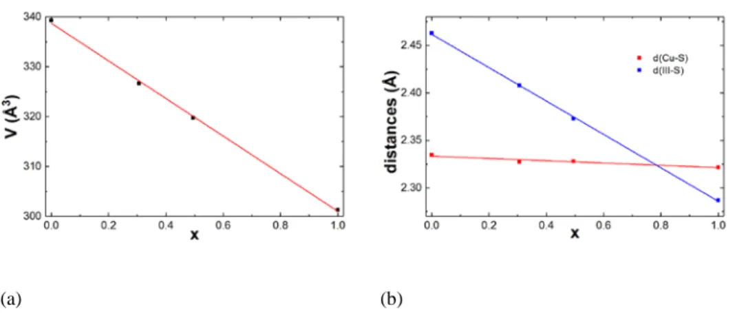
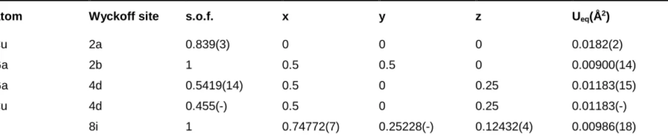
When Ga is substituted for In, the unit cell volume decreases (see Figure 3.8a), consistent with the fact that the Ga-S bonds are shorter than the In-Ga-S ones. In addition, the position of the sulfur atom is slightly shifted towards x≈0.25. Consequently, the Cu-S bond length is roughly constant (Figure 3.8b) meaning that the bond valence of copper is also constant, very close to 1, along the series. The chalcopyrite structure is flexible enough to accommodate quite large metal(III)-S bond distance variation from 2.46 Å in CuInS2 to 2.29 Å in CuGaS2. It is worth noting that in these sulfides, the Metal-S bond distances cannot not be well evaluated from ionic radii, the concept of bond valence56,57 is much more suited.
(a) (b)
Figure 3.8: Evolution of the unit cell volume (a) and the Cu-S bond distance (b) in the Cu(In1-xGax)S2 series from single crystal X-ray diffraction analyses.
4.2
CuInS
2- In
2S
3system
In the literature, the Cu2S - In2S3 pseudo-binary system (Cu1-zIn1+z/3S2) has been well investigated. Here again, charge balance is maintained in the formula through the decrease of Cu(I) (minus z value) and the corresponding increase of In(III) (plus z/3 value). The first published results indicate a large 2-phase region between CuInS2 and CuIn5S858. A tentative temperature-composition phase diagram in the Cu2S-In2S3 system, published by Binsma49, also shows the ab-sence of a single phase in a large composition range between CuInS2 (chalcopyrite) and CuIn5S8 (thiospinel) at room temperature. This large 2-phase feature has recently been confirmed and the limit of the chalcopyrite phase domain has been found in the range of 0 ≤ z ≤ 0.09 (see Figure 3.9)59. Additionally, slightly copper-rich (relative to CuInS
2) samples were shown to comprise stoichiometric CuInS2 and binary copper sulfides.
Figure 3.9: Phase diagram on the Cu2S - CuIn5S8 line showing the large 2-phase domain between Cu0.91In1.03S2 with the chalco-pyrite structure and CuIn5S8 (equivalent to Cu0.25In1.25S2) with the thiospinel structure.
It is worth noting that, unlike for copper-indium selenides (CISe) compounds, the specific composition of CuIn3X5 definitely does not exist for sulfides (X=S). Thus, if CIS thin films are prepared in copper-poor conditions, to avoid the formation of copper sulfide, it is very likely that the film will contain the cubic thiospinel CuIn5S8 compound. In the crystal structure of this compound, copper atoms share two distinct tetrahedral sites with a part of indium atoms (4a and 4c sites) while the remaining indium atoms are located on the 16e octahedral site in the F-43m cubic space group60. The
crystal structure difference between chalcopyrite and thiospinel gives rise to very different electronic properties. For instance, the CuIn5S8 compound is found to be a n-type semiconductor and to be detrimental to the PV application61.
From a sample with target composition of Cu0.70In1.10S2 (i.e. z = 0.30) a single crystal of the thiospinel phase was used for X-ray diffraction experiment. The obtained crystal structure is very close to that given in the literature but with a slight difference on the distribution of copper and indium atoms on the 4a and 4c tetrahedral sites (F-43m space group). The copper/indium site occupancy factors (s.o.f.) are 4a 0.30/0.70 and 4c 0.70/0.30, instead of 4a 0.52/0.48 and 4c 0.48/0.52 as published by Gastaldi60. This discrepancy may originate from distinguishable synthesis conditions.
4.3
CuGaS
2- Ga
2S
3system
From the literature, it is clear that the copper-gallium sulfides (CGS) behave very differently than the copper indium ones62–64. First, the compounds of interest (Cu1-zGa1+z/3S2 with 0 ≤ z ≤ 0.75) all adopt a tetragonal crystal structure in which copper and gallium are in tetrahedral environments (while In may accept Td and Oh chemical environments). Copper and gallium are hard to be distinguished by conventional X-ray diffraction, this feature could explain some discrepancies into the literature about the actual crystal structure of these compounds. Then we decided to re-investigate the CuGaS2-CuGa5S8 system especially through the single crystal X-ray diffraction technique. The tetragonal symmetry for all the studied crystals is confirmed. On the other hand, for a slight copper-poor CGS compound (target composition of Cu0.90Ga1.03S2) is was found that several hhl reflections with the condition 2h+l = 2n+1 are to be definitely classified as observed reflections since their intensities are larger than 3 times their standard deviations (see Table 2). Thus the I2d space group has to be discarded for this crystal. The structure was then refined with the stannite model, space group I4_ 2m, in which copper and gallium share the 4d crystallographic position. In order to ensure the charge equilibrium, the copper deficiency (mainly located on the 2a position) is compensated by a gallium excess on 4d. The crystal structure parameters are gathered in Table 3. The refined composition is Cu0.874Ga1.042S2.
Table 2: Some of the strongest forbidden reflections in the I4 _
2d space group for a crystal with composition close to Cu0.90Ga1.03S2. These reflections cannot definitely be considered as absent reflections.
h k l I σ(I) I/σ (I) 1 1 4 266.8 6.5 41.0 0 0 6 326.8 12.6 25.8 1 1 4 346.1 15.4 22.4 0 0 6 355.6 16.8 21.2 -2 2 6 223.8 11.5 19.5
Table 3: Main structural parameters for a crystal with refined composition of Cu0.874Ga1.042S2 in the I4 _
2m space group (#121). Residual factors R(obs)/R(all) = 2.07/3.92, goodness of fit = 1.15, Fourier-difference largest peaks: 0.50/-0.69 e-/Å3, reflections obs/all 241/368, 16 refined parameters. In order to fulfill the charge balance equilibrium, the normalized occupancies (ai) of cop-per and gallium are restrained according to the equation ai[Cu(4d)]=1-ai[Cu(2a)]-3*ai[Ga(2b)]-3*ai[(Ga(4d)], where ai=sof×site multiplicity/general multiplicity. In the I4
_
2m space group, the general multiplicity is 16.
Atom Wyckoff site s.o.f. x y z Ueq(Å2)
Cu 2a 0.839(3) 0 0 0 0.0182(2)
Ga 2b 1 0.5 0.5 0 0.00900(14)
Ga 4d 0.5419(14) 0.5 0 0.25 0.01183(15) Cu 4d 0.455(-) 0.5 0 0.25 0.01183(-) S 8i 1 0.74772(7) 0.25228(-) 0.12432(4) 0.00986(18)
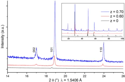
For very copper-poor compositions, i.e. z = 0.60 (CuGa3S5) and z = 0.75 (CuGa5S8) the powder diffraction patterns clearly show the presence of 002 and 110 reflections with their intensities increasing with copper deficiency (Figure 3.10). The structure of these compounds have been refined with the stannite model already proposed by Maeda63. Addi-tional samples have been prepared with intermediate compositions z in the range of 0.60-0.75. They are found to be of
pure phases meaning that a solid solution occurs in the composition range z = 0.60 - 0.75. Because copper and gallium have very close crystallographic behavior, the Cu/Ga distribution on the cationic sites of the stannite structure can vary in a large range according the composition as soon as the charge equilibrium is achieved: 3Cu+ ⇔ Ga3+ + 2V
Cu. In the case of intermediate copper-poor target compositions (0.10 < z < 0.60), the corresponding powder patterns can be indexed with two unit-cells, close to that of Cu0.90Ga1.03S2 (z = 0.10) and Cu0.40Ga1.20S2 (z = 0.60), see Figure 3.11). It is worth nothing that this 2-phase feature disappears if the sample is quenched from 800°C to room temperature at the end of the synthesis procedure.
Figure 3.10: Powder X-ray diffraction pattern of CuGaS2 (with chalcopyrite structure) and 2 very copper-poor CGS compounds with z = 0.60 and 0.70 (with stannite structure). The labelled reflections are forbidden in the chalcopyrite structure.
Figure 3.11: Powder X-ray diffraction pattern of slight Cu-poor (z=0.10) Cu-poor (z=0.30) and very Cu-poor (z=0.60) CGS sam-ples. The 2-phase nature of the sample with intermediate composition is emphasized in the low-2θ zoom (see inset).
4.4
Copper-poor CIGS compounds
Let us consider now the Cu2S - In2S3 - Ga2S3 ternary system where CIGS samples are copper-poor and contain both indium and gallium as trivalent element, corresponding to the general formulation: Cu1-z(In1-xGax)1+z/3S2, with 0 < x < 1 and 0 < z ≤ 0.60. So far, no information about theses compositions are reported in the literature. From the observation of powder-ray diffraction patterns, the main conclusion is that all these prepared materials were no pure-phase. In other words, as soon as the target composition is copper-poor, the obtained powdered sample is, at least, formed of two phases sample. Hence, for the targeted Cu0.70(In0.70Ga0.30)1.10S2 (x = 0.30, z = 0.30) composition, two compounds can be detected on the backscattered electron SEM image (Figure 3.12). From the EDX analyses, the actual compositions of the 2 phases
in equilibrium are Cu0.96(4)In0.61(3)Ga0.39(1)S2.00(2) (x = 0.39, z = 0.04) and Cu0.41(2)In0.93(3)Ga0.26(1)S2.00(1) (x = 0.26, z = 0.59). It is worth noticing that the almost stoichiometric Cu(In,Ga)S2 phase contains more (less) gallium (indium) than the copper-poor one. The 2-phase nature of Cu0.3(In0.7Ga0.3)1+z/3S2 samples (z = 0, 0.21, 0.30, 0.60) was confirmed by powder XRD analyses. Figure 3.13 gives the X-ray diffraction patterns of samples with target compositions of Cu0.79(In0.70Ga0.30)1.07S2 (x = 0.30, z = 0.21) and Cu0.70(In0.70Ga0.30)1.10S2 (x = 0.30, z = 0.30) compared to those of the single phase samples with compositions close to Cu(In0.70Ga0.30)S2 (chalcopyrite crystal structure) and Cu0.40(In0.70Ga0.30)1.20S2 (trigonal structure, see next section). One can definitely conclude that there is a large miscibility gap for 0.04 < z < 0.60 for mixed In/Ga CIGS compounds.
Figure 3.12: SEM backscattered electron micrograph of sample with target composition of x=0.30 and z=0.30 showing the equi-librium between an almost stoichiometric phase (Cu0.96In0.61Ga0.39S2 in dark grey) and a very copper poor one (Cu0.41In0.93Ga0.26S2 in light grey).
Figure 3.13: Powder X-ray diffraction pattern of CIGS samples with target compositions of z=0, 0.21, 0.30 and 0.60. The z=0 pattern can be indexed in the chalcopyrite crystal structure while the z=0.60 pattern corresponds to a trigonal phase. The sam-ples with intermediate compositions are clearly a mixing of these two phases.
4.5
Very copper-poor In/Ga phases
As already mentioned attempts to synthesize Cu1-z(In1-xGax)1 + z/3S2 compounds systematically lead to multi-phase-samples for z> 0.1 with the formation of very copper-poor new CIGS compounds. To solve the structure of these new quaternary compounds, four suitable crystals were picked up in powdered samples with the targeted Cu0.7(In0.7Ga03)1.1S2 (z=0.3, x=0.3), Cu0.4(In0.7Ga0.3)1.2S2 (z=0.6, x=0.3) and Cu0.4(In0.5Ga0.5)1.2S2 (z=0.6, x=0.5) compositions65. Four layered
structure-types, depicted in Figure 3.14, were then identified and named CIGS4, CIGS5, CIGS6 and CIGS7. In the CIGSn notations, n corresponds to the number of anionic layers of the slab. Two consecutive slabs are separated by a van der Waals gap. The EDX analyses concluded to Cu0.32In1.74Ga0.84S4 (CIGS4-type), Cu0.65In1.75Ga1.4S5 (CIGS5-type), Cu1.44In2.77Ga0.76S6 (CIGS6-type) and Cu1.1In2.49Ga1.8S7 (CIGS7-type) chemical compositions.All the structures exhibit a 2D-character with layers built upon (InS6) octahedra sharing edges on which condense on both side 1, 2 or 3 layers made of (MS4) tetrahedra (M = Cu, In, Ga) sharing corner. This generic formulae can then be written (M(Td))n-2(In(Oh))Sn. Cell parameters for all compounds are given in Table 4.
For all structures, the octahedral sites (Oh) are exclusively and fully occupied by indium atoms. Contrarily, tetrahe-dral sites (Td) can be partially vacant and a mixed occupancy is often observed. Interatomic distances match with those reported in the literature for phases with similar chemical environments49,63,66. As expected, the In-S bond distances in octahedral site (∼2.6 Å) are larger than the In-S bonds in tetrahedral environment (∼2.4 Å) that are larger than Cu(Ga)-S ones (∼2.3 Å). The presence of cationic vacancies leads systematically to a slight shortening of the mean cation-sulfur bond distances compared to the expected ones. The vacancy rate of Td sites never exceeds 20% except for CIGS7 in which a mixed site (In-Cu) exhibits a vacancy rate of 50%. It is also worth noticing that indium atoms in tetrahedral sites are preferentially located at the van de Waals gap frontier, probably for steric reasons.
CIGS4, CIGS5 and CIGS6 structure-types with Td(Cu,In,Ga, )-Oh(In)-Td(Cu,In,Ga, ), (Td(In,Ga)-Td(Cu,Ga, )-Oh(In)-Td(Cu,In)) and (Td(Cu,Ga)-Td(Ga,In, )-Oh(In)-Td(Cu,Ga)-Td(Ga,In, )) sequences are isostructural to ZnIn2S4-type I, Zn2In2S5-type IIa and Zn3In2S6, respectively67. The CIGS5 stacking type has been also already observed for Ag1.25Ga2.5In3.75S1068. Conversely CIGS7 (Td(In,Ga)-Td(Cu,In, )-Td(Ga, )-Oh(In)-Td(In,Ga)-Td(Cu)) exhibits an unprecedented layered stacking.
Figure 3.14: Polyhedra representation of the structure for Cu0.32In1.74Ga0.84S4 (CIGS4) Cu0.65In1.75Ga1.4S5 (CIGS4), Cu1.44In2.77Ga0.76S6 and Cu1.1In2.49Ga1.8S7 compounds.
Table 4: Cell parameters for CIGSn phases
CIGS4 CIGS5 CIGS6 CIGS7
a (Å) 3.8203(6) 3.7898(2) 3.8506(2) 3.7933(3) c (Å) 12.182(2) 30.664(3) 18.704(2) 21.540(14) S G P-3m1 P63mc P-3m1 P3m1
Due to the strong structural similarity in between (M(Td))n-2In(Oh) Sn blocks and on the other hand to the 2D character of these building entities, intergrowths and stacking faults could exist. In fact, the quality of the single crystals was often poor and the proposed structural models (CIGS4, CIGS5, CIGS6 and CIGS7) should probably be considered as average structures. Due the multiple possibilities to distribute cations over tetrahedral sites, these materials are subject to chem-ical composition deviations (In/Ga) which open up an avenue for the stabilization of new materials. To illustrate this purpose, in Figure 3.15, the HAADF-STEM image of a faulted crystal and its corresponding [100] electron diffraction pattern are shown. The streaking of diffraction spots observed along c*-axis testify of a strong structural disorder. In addition, the Z-contrast image (HAADF-STEM) figures out intergrowths. The In-based octahedral layers appear as brighter spots rows and tetrahedral (MS4) ones like gray rows. The van der Waals gap is imaged as a dark area. The number of tetrahedral layers on each side of the In-based layers can be then easily counted and the different members of the series (M(Td))n-2(In(Oh))Sn can thus be identified (see annotations in Figure 3.15).
Figure 3.15: HAADF-STEM image of a faulted crystal highlighting the propensity of (M(Td))n-2(In(Oh))Sn materials to contain inter-growth defects (the structure-type, according to the CIGSn notation is given for each slab). The van der Waals gaps are imaged as dark contrast lines. The inset gives the corresponding [100] electron diffraction pattern.
4.6
CIGS phase diagram
Taking into account all the above presented results (combined with data from literature), we can now propose a ternary phase diagram for the Cu2S-In2S3-Ga2S3 system59 limited to the copper-poor side of the stoichiometric line CuInS2-CuGaS2 (see Figure 3.16). As detailed above, except for the indium-free compounds (i.e. Cu1-zGa1+z/3S2) the te-tragonal structure (either chalcopyrite or stannite) with only tetrahedral cationic environments definitely does not exist for copper-poor compositions. For such target compositions, the obtained samples are made of at least two phases: a phase close to stoichiometry Cu(In,Ga)S2 is systematically in equilibrium with a very copper-poor one. The main struc-tural feature of these very-copper poor phases is the distribution of indium both on tetrahedral and octahedral sites while Cu and Ga remain with tetrahedral coordination65.
As already indicated, the aim of this investigation on CIGS sulfide materials was their potential application as top cell in a silicon based tandem solar cell. Although this concept is quite simple, the gain in energy conversion efficiency
compared to the silicon based single junction needs to have a high efficient top cell with efficiencies close to 20%69. This target is very challenging taking into account that for CIGSSe material the performance rapidly drops when the bandgap increases70. Even though cell efficiencies up to 10% have been achieved with pure sulfide CIGS based solar cells for quite a long time71, the record is, nowadays, just above 15%72 which is far below the efficiencies for the selenide CIGSe counterpart materials (> 23%). We have investigated crystal chemistry issues which can be correlated to this large difference between sulfide and selenide. The proposed ternary phase diagram definitely shows that mixed In/Ga copper-poor CIGS materials do not exist with a tetragonal symmetry (in contrast with selenide derivatives). In other words, as soon as the prepared composition is Cu-poor, the resulting sample corresponds to the equilibrium of an almost stoichiometric phase and very copper-poor phases with other crystal structures. Thus, in the case of thin films prepara-tion, the control of the synthesis conditions has to be very precise to obtain single phase materials.
Figure 3.16: CIGS ternary phase diagram. The single phase domains (according EDX and PXRD analyzes) are indicated in blue. The hatched area indicates the poly-phase domain. The high gallium content domain has not been studied, except the indium free CGS line.
5 Summary
Due to the very strong dependence of properties of a material with its composition and its structural arrangement, much attention has to be devoted to its characterization. Indeed, for solid state chemists, crystal chemistry is the essence of their work. Once the long range ordering of atoms is determined, physical characteristics can be anticipated, and change in composition may be envisioned if needed to achieve desired properties. For sure, materials contain naturally intrinsic defects which may drastically impact their properties. These defects are in so low concentration that they request specific techniques to be identified and quantified (out of the scope of a crystal chemistry investigation). Nevertheless, crystal X-ray analyses can be appropriate to account defect in larger concentration, specifically when crystal sites are randomly occupied. If scattering factor are quite different, regular single crystal analyses are sufficient. On the contrary, resonant X-ray (or neutron) diffraction may be requested to distinguish ions with identical (or almost identical) electronic configuration but this requires facility access to a synchrotron radiation (or neutron) source. Nevertheless, let us mention that much information can be extracted from a careful crystal analysis with a conventional X-ray diffraction source in laboratory if characteristics of chemical species are taken into account, e.g. their oxidation states, their preferential chem-ical environment or their ionic radius. NMR is a powerful complementary technique to X-ray diffraction to get local information. Whatever, when both techniques are coupled, a better characterization of the materials is achievable that can be extrapolated to thin films and photovoltaic devices.
As illustrations of the above general description of the crystal chemistry approach, this chapter is dealing with the investigation of two compounds which can be used as absorber in thin film solar cells. In the case of CZTS material, we have shown how advanced characterization techniques (resonant single crystal X-ray diffraction and solid state NMR
spectroscopy) can help to understand the complex Cu/Zn distribution. Additionally, this study has shown that copper-poor CZTS compounds are less prone to Cu/Zn disorder than the stoichiometric Cu2ZnSnS4. This point can be correlated to the better photovoltaic performances obtained with such copper-poor CZTS absorbers. On the other hand, the inves-tigation of the Cu2S-In2S3-Ga2S3 system pseudo-ternary system illustrates the importance of careful structural determi-nations coupled to precise chemical composition analyses in order to evaluate the ability of such compounds to accom-modate with copper deficiencies. For compositions of interest for tandem solar cells (i.e. Ga/(Ga+In) close to 0.3) the single phase stability domain is shown to be very narrow. The consequence is that for thin film preparations, the control of the synthesis conditions has to be very precise to obtain single phase materials.
According to the literature, both for CZTS and CIGS compounds, selenides lead always to better photovoltaic effi-ciencies than the sulfide counterparts. This fact is likely correlated to the higher structural flexibility of selenides which can keep the tetrahedral metal coordination in a wide copper-composition range.
6 Acknowledgements
The results presented in this chapter are parts of the PhD thesis of Léo Choubrac, Pierre Bais and Angélica Thomere. The authors acknowledge them for their contributions. Many thanks also to Nicolas Barreau for fruitful discussions about the preparation of thin film CIGS solar cells.
This work was supported by different research programs, namely NovACEZ ANR-10-HABISOL-008 and ANRI-EED-002-01 from the French Government. The French National Centre for Scientific Research (CNRS), the University of Nantes, the Région Pays de la Loire, the Synchrotron Soleil, the Institut Photovoltaïque d'Ile-de-France (IPVF) and the French Electricity Company (EDF) are also thanked for the financial supports.
References
(1) Global Market Outlook 2018-2022, https://www.solarpowereurope.org/global-market-outlook-2018-2022/ (accessed March 16 2020).
(2) Ito, K.; Nakazawa, T. Electrical and Optical Properties of Stannite-Type Quaternary Semiconductor Thin Films. Japanese Journal of Applied Physics 1988, 27, 2094–2097.
(3) Woods-Robinson, R.; Han, Y.; Zhang, H.; Ablekim, T.; Khan, I.; Persson, K.; Zakutayev, A. Review of Wide Band Gap Chalcogenide Semiconductors. arXiv:1910.08153 [cond-mat] 2020.
(4) Bodnar, I. V.; Lukomskii, A. I. The Concentration Dependence of the Band Gap for CuGaxIn1-XS2 and AgGaxIn1-xS2 Solid Solutions. physica status solidi (a) 1986, 98 (2), K165–K169. https://doi.org/10.1002/pssa.2210980255.
(5) Nakamura, M.; Yamaguchi, K.; Kimoto, Y.; Yasaki, Y.; Kato, T.; Sugimoto, H. Cd-Free Cu(In,Ga)(Se,S)2 Thin-Film Solar Cell With Record Efficiency of 23.35%. IEEE Journal of Photovoltaics 2019, 9 (6), 1863–1867.
https://doi.org/10.1109/JPHOTOV.2019.2937218.
(6) First Solar Achieves Yet Another Cell Conversion Efficiency World Record https://investor.firstsolar.com/news/press-re-lease-details/2016/First-Solar-Achieves-Yet-Another-Cell-Conversion-Efficiency-World-Record/default.aspx (accessed Jan 31, 2020).
(7) Katagiri, H.; Sasaguchi, N.; Hando, S.; Hoshino, S.; Ohashi, J.; Yokota, T. Preparation and Evaluation of Cu2ZnSnS4 Thin Films by Sulfurization of E-B Evaporated Precursors. Solar Energy Materials and Solar Cells 1997, 49 (1–4), 407–414. https://doi.org/10.1016/S0927-0248(97)00119-0.
(8) Shockley, W.; Queisser, H. J. Detailed Balance Limit of Efficiency of P‐n Junction Solar Cells. Journal of Applied Physics
1961, 32 (3), 510–519. https://doi.org/10.1063/1.1736034.
(9) Vos, A. D. Detailed Balance Limit of the Efficiency of Tandem Solar Cells. J. Phys. D: Appl. Phys. 1980, 13 (5), 839–846. https://doi.org/10.1088/0022-3727/13/5/018.
(10) Bernardini, G. P.; Borrini, D.; Caneschi, A.; Di Benedetto, F.; Gatteschi, D.; Ristori, S.; Romanelli, M. EPR and SQUID Mag-netometry Study of Cu2FeSnS4 (Stannite) and Cu2ZnSnS4 (Kesterite). Phys. Chem. Miner. 2000, 27 (7), 453–461. https://doi.org/10.1007/s002690000086.
(11) Schorr, S.; Höhne, R.; Wagner, G.; Riede, V.; Kockelmann, W. Investigation of the Solid Solution Series 2(MnX)–CuInX2 (X=S, Se). Journal of Physics and Chemistry of Solids 2005, 66 (11), 1966–1969.
https://doi.org/10.1016/j.jpcs.2005.09.066.
(12) Petříček, V.; Dušek, M.; Palatinus, L. Crystallographic Computing System JANA2006: General Features. Z. Kristallogr.
2014, 229 (5), 345–352. https://doi.org/10.1515/zkri-2014-1737.
(13) Hodeau, J.-L.; Favre-Nicolin, V.; Bos, S.; Renevier, H.; Lorenzo, E.; Berar, J.-F. Resonant Diffraction. Chem. Rev. 2001,
101 (6), 1843–1868. https://doi.org/10.1021/cr0000269.
(14) Schorr, S.; Hoebler, H. J.; Tovar, M. A Neutron Diffraction Study of the Stannite-Kesterite Solid Solution Series. Eur. J.
Min-eral. 2007, 19 (1), 65.
(15) Laugier, J. Dispano; 1999.
(16) Lafond, A.; Choubrac, L.; Guillot-Deudon, C.; Fertey, P.; Evain, M.; Jobic, S. X-Ray Resonant Single-Crystal Diffraction Technique, a Powerful Tool to Investigate the Kesterite Structure of the Photovoltaic Cu2ZnSnS4 Compound. Acta Crystal-lographica Section B Structural Science, Crystal Engineering and Materials 2014, 70 (2), 390–394.
https://doi.org/10.1107/S2052520614003138.
(17) Larsen, F. H.; Jakobsen, H. J.; Ellis, P. D.; Nielsen, N. Chr. QCPMG-MAS NMR of Half-Integer Quadrupolar Nuclei. Journal
of Magnetic Resonance 1998, 131 (1), 144–147. https://doi.org/10.1006/jmre.1997.1341.
(18) Hung, I.; Gan, Z. On the Practical Aspects of Recording Wideline QCPMG NMR Spectra. Journal of Magnetic Resonance
2010, 204 (2), 256–265. https://doi.org/10.1016/j.jmr.2010.03.001.
(19) Paris, M.; Larramona, G.; Bais, P.; Bourdais, S.; Lafond, A.; Choné, C.; Guillot-Deudon, C.; Delatouche, B.; Moisan, C.; Dennler, G. 119Sn MAS NMR to Assess the Cationic Disorder and the Anionic Distribution in Sulfoselenide Cu2ZnSn(SxSe1– x)4 Compounds Prepared from Colloidal and Ceramic Routes. J. Phys. Chem. C 2015, 119 (48), 26849–26857.
https://doi.org/10.1021/acs.jpcc.5b08938.
(20) Nakayama, N.; Ito, K. Sprayed Films of Stannite Cu2ZnSnS4. Applied Surface Science 1996, 92, 171–175. https://doi.org/10.1016/0169-4332(95)00225-1.
(21) Wang, W.; Winkler, M. T.; Gunawan, O.; Gokmen, T.; Todorov, T. K.; Zhu, Y.; Mitzi, D. B. Device Characteristics of CZTSSe Thin-Film Solar Cells with 12.6% Efficiency. Adv. Energy Mater. 2014, 4 (7), 1301465.
https://doi.org/10.1002/aenm.201301465.
(22) Rau, U.; Werner, J. H. Radiative Efficiency Limits of Solar Cells with Lateral Band-Gap Fluctuations. Applied Physics
Let-ters 2004, 84 (19), 3735–3737. https://doi.org/doi:10.1063/1.1737071.
(23) Scragg, J. J. S.; Larsen, J. K.; Kumar, M.; Persson, C.; Sendler, J.; Siebentritt, S.; Björkman, C. P. Cu–Zn Disorder and Band Gap Fluctuations in Cu2ZnSn(S,Se)4: Theoretical and Experimental Investigations. physica status solidi (b) 2016, 253 (2), 247–254. https://doi.org/10.1002/pssb.201552530.
(24) Quennet, M.; Ritscher, A.; Lerch, M.; Paulus, B. The Order-Disorder Transition in Cu2ZnSnS4: A Theoretical and Experi-mental Study. Journal of Solid State Chemistry 2017, 250, 140–144. https://doi.org/10.1016/j.jssc.2017.03.018. (25) Scragg, J. J.; Ericson, T.; Kubart, T.; Edoff, M.; Platzer-Björkman, C. Chemical Insights into the Instability of Cu2ZnSnS4
(26) Buffière, M.; Brammertz, G.; Batuk, M.; Verbist, C.; Mangin, D.; Koble, C.; Hadermann, J.; Meuris, M.; Poortmans, J. Micro-structural Analysis of 9.7% Efficient Cu2ZnSnSe4 Thin Film Solar Cells. Applied Physics Letters 2014, 105 (18), 183903. https://doi.org/10.1063/1.4901401.
(27) Hall, S. R.; Szymanski, J. T.; Stewart, J. M. Kesterite, Cu2(Zn,Fe)SnS4, and Stannite, Cu2(Fe,Zn)SnS4 Structurally Similar but Distinct Minerals. Can. Mineral. 1978, 16 (2), 131.
(28) Schorr, S. Crystallographic Aspects of Cu2ZnSnS4 (CZTS). In Copper Zinc Tin Sulfide-Based Thin-Film Solar Cells; John Wiley & Sons, Ltd, 2015; pp 53–74. https://doi.org/10.1002/9781118437865.ch3.
(29) Chen, S.; Yang, J. H.; Gong, X. G.; Walsh, A.; Wei, S. H. Intrinsic Point Defects and Complexes in the Quaternary Kesterite Semiconductor Cu2ZnSnS4. Phys. Rev. B 2010, 81 (24), 245204.
(30) Kosyak, V.; Postnikov, A. V.; Scragg, J.; Scarpulla, M. A.; Platzer-Björkman, C. Calculation of Point Defect Concentration in Cu2ZnSnS4: Insights into the High-Temperature Equilibrium and Quenching. Journal of Applied Physics 2017, 122 (3), 035707. https://doi.org/10.1063/1.4994689.
(31) Cox, P. A. Transition Metal Oxides: An Introduction to Their Electronic Structure and Properties; Oxford University Press,
2010.
(32) Fontané, X.; Izquierdo-Roca, V.; Saucedo, E.; Schorr, S.; Yukhymchuk, V. O.; Valakh, M. Ya.; Pérez-Rodríguez, A.; Mo-rante, J. R. Vibrational Properties of Stannite and Kesterite Type Compounds: Raman Scattering Analysis of
Cu2(Fe,Zn)SnS4. Journal of Alloys and Compounds 2012, 539, 190–194. https://doi.org/10.1016/j.jallcom.2012.06.042. (33) Levcenko, S.; Tezlevan, V. E.; Arushanov, E.; Schorr, S.; Unold, T. Free-to-Bound Recombination in near Stoichiometric
Cu_{2}ZnSnS_{4} Single Crystals. Phys. Rev. B 2012, 86 (4), 045206. https://doi.org/10.1103/PhysRevB.86.045206. (34) Valakh, M. Y.; Kolomys, O. F.; Ponomaryov, S. S.; Yukhymchuk, V. O.; Babichuk, I. S.; Izquierdo-Roca, V.; Saucedo, E.;
Perez-Rodriguez, A.; Morante, J. R.; Schorr, S.; Bodnar, I. V. Raman Scattering and Disorder Effect in Cu2ZnSnS4. physica
status solidi (RRL) – Rapid Research Letters 2013, 7 (4), 258–261. https://doi.org/10.1002/pssr.201307073.
(35) Schorr, S. The Crystal Structure of Kesterite Type Compounds: A Neutron and X-Ray Diffraction Study. Solar Energy
Mate-rials and Solar Cells 2011, 95 (6), 1482–1488. https://doi.org/10.1016/j.solmat.2011.01.002.
(36) Choubrac, L.; Paris, M.; Lafond, A.; Guillot-Deudon, C.; Rocquefelte, X.; Jobic, S. Multinuclear (67Zn, 119Sn and 65Cu) NMR Spectroscopy – an Ideal Technique to Probe the Cationic Ordering in Cu2ZnSnS4 Photovoltaic Materials. Phys. Chem.
Chem. Phys. 2013, 15, 10722. https://doi.org/10.1039/C3CP51320C.
(37) Scragg, J. J. S.; Choubrac, L.; Lafond, A.; Ericson, T.; Platzer-Björkman, C. A Low-Temperature Order-Disorder Transition in Cu2ZnSnS4 Thin Films. Applied Physics Letters 2014, 104 (4), 041911. https://doi.org/10.1063/1.4863685.
(38) Timmo, K.; Kauk-Kuusik, M.; Pilvet, M.; Raadik, T.; Altosaar, M.; Danilson, M.; Grossberg, M.; Raudoja, J.; Ernits, K. Influ-ence of Order-Disorder in Cu2ZnSnS4 Powders on the Performance of Monograin Layer Solar Cells. Thin Solid Films 2017,
633, 122–126. https://doi.org/10.1016/j.tsf.2016.10.017.
(39) Bais, P.; Caldes, M. T.; Paris, M.; Guillot-Deudon, C.; Fertey, P.; Domengès, B.; Lafond, A. Cationic and Anionic Disorder in CZTSSe Kesterite Compounds: A Chemical Crystallography Study. Inorg. Chem. 2017, 56 (19), 11779–11786. https://doi.org/10.1021/acs.inorgchem.7b01791.
(40) Lafond, A.; Guillot-Deudon, C.; Vidal, J.; Paris, M.; La, C.; Jobic, S. Substitution of Li for Cu in Cu2ZnSnS4: Toward Wide Band Gap Absorbers with Low Cation Disorder for Thin Film Solar Cells. Inorg. Chem. 2017, 56 (5), 2712–2721. https://doi.org/10.1021/acs.inorgchem.6b02865.
(41) Pogue, E. A.; Paris, M.; Sutrisno, A.; Lafond, A.; Johnson, N.; Shoemaker, D. P.; Rockett, A. A. Identifying Short-Range Disorder in Crystalline Bulk Cu2SnS3 Phases: A Solid-State Nuclear Magnetic Resonance Spectroscopic Investigation.
Chem. Mater. 2018. https://doi.org/10.1021/acs.chemmater.8b01182.
(42) Choubrac, L.; Lafond, A.; Paris, M.; Guillot-Deudon, C.; Jobic, S. The Stability Domain of the Selenide Kesterite Photovol-taic Materials and NMR Investigation of the Cu/Zn Disorder in Cu2ZnSnSe4 (CZTSe). Phys. Chem. Chem. Phys. 2015. https://doi.org/10.1039/C5CP01709B.
(43) Paris, M.; Choubrac, L.; Lafond, A.; Guillot-Deudon, C.; Jobic, S. Solid-State NMR and Raman Spectroscopy To Address the Local Structure of Defects and the Tricky Issue of the Cu/Zn Disorder in Cu-Poor, Zn-Rich CZTS Materials. Inorg.
Chem. 2014, 53 (16), 8646–8653. https://doi.org/10.1021/ic5012346.
(44) Ritscher, A.; Hoelzel, M.; Lerch, M. The Order-Disorder Transition in Cu2ZnSnS4 – A Neutron Scattering Investigation.
Jour-nal of Solid State Chemistry 2016, 238, 68–73. https://doi.org/10.1016/j.jssc.2016.03.013.
(45) Rudisch, K.; Ren, Y.; Platzer-Björkman, C.; Scragg, J. Order-Disorder Transition in B-Type Cu2ZnSnS4 and Limitations of Ordering through Thermal Treatments. Appl. Phys. Lett. 2016, 108 (23), 231902. https://doi.org/10.1063/1.4953349. (46) Kandare, S. P.; Dahiwale, S. S.; Dhole, S. D.; Rao, M. N.; Rao, R. Order-Disorder Transition in Nano-Cu2ZnSnS4: A Raman
Spectroscopic Study. Materials Science in Semiconductor Processing 2019, 102, 104594. https://doi.org/10.1016/j.mssp.2019.104594.
(47) Essig, S.; Steiner, M. A.; Allebé, C.; Geisz, J. F.; Paviet-Salomon, B.; Ward, S.; Descoeudres, A.; LaSalvia, V.; Barraud, L.; Badel, N.; Faes, A.; Levrat, J.; Despeisse, M.; Ballif, C.; Stradins, P.; Young, D. L. Realization of GaInP/Si Dual-Junction Solar Cells With 29.8% 1-Sun Efficiency. IEEE Journal of Photovoltaics 2016, 6 (4), 1012–1019.
https://doi.org/10.1109/JPHOTOV.2016.2549746.
(48) Souilah, M.; Lafond, A.; Guillot-Deudon, C.; Harel, S.; Evain, M. Structural Investigation of the Cu2Se–In2Se3–Ga2Se3 Phase Diagram, X-Ray Photoemission and Optical Properties of the Cu1−z(In0.5Ga0.5)1+z/3Se2 Compounds. J. Solid
State Chem. 2010, 183 (10), 2274–2280. https://doi.org/10.1016/j.jssc.2010.08.014.
(49) Binsma, J. J. M.; Giling, L. J.; Bloem, J. Phase Relations in the System Cu2S-In2S3. Journal of Crystal Growth 1980, 50 (2), 429–436. https://doi.org/10.1016/0022-0248(80)90090-1.
(50) Yamamoto, N.; Miyauchi, T. Growth of Single Crystals of CuGaS2 and CuGa1-xInxS2 in In Solution. Jpn. J. Appl. Phys. 1972,
11 (9), 1383. https://doi.org/10.1143/JJAP.11.1383.
(51) Stephan, C. Structural Trends in off Stoichiometric Chalcopyrite Type Compound Semiconductors, Freie Universität Berlin, Freie Universität Berlin, Germany, 2011.
(52) Bodnar, I. V.; Bologa, A. P.; Korzun, B. V.; Makovetskaya, L. A. Melting Temperatures of the AIBIIICVI2-Type (AI-Cu, Ag; BIII-Al, Ga, In; CVI-S, Se) Compounds and Phase Diagrams of Their Solid Solutions. Thermochimica Acta 1985, 93, 685– 688. https://doi.org/10.1016/0040-6031(85)85172-8.
(53) Marushko, L. P.; Romanyuk, Y. E.; Piskach, L. V.; Parasyuk, O. V.; Olekseyuk, I. D.; Volkov, S. V.; Pekhnyo, V. I. The Re-ciprocal System CuGaS2 + CuInSe2 ⇌ CuGaSe2 + CuInS2. Chemistry of metals and alloys 2010, 3, 18–23.
(54) Kato, T.; Hayashi, S.; Kiuchi, T.; Ishihara, Y.; Nabetani, Y.; Matsumoto, T. Structural Properties of Cu(Ga1−xInx)YSz Bulk Alloys. Journal of Crystal Growth 2002, 237–239, 2005–2008. https://doi.org/10.1016/S0022-0248(01)02304-1.
(55) Oishi, K.; Yoneda, K.; Yoshida, O.; Yamazaki, M.; Jimbo, K.; Katagiri, H.; Araki, H.; Kobayashi, S.; Tsuboi, N. Characteriza-tion of Cu(In,Ga)S2 Crystals Grown from the Melt. Thin Solid Films 2007, 515 (15), 6265–6268.
https://doi.org/10.1016/j.tsf.2006.12.145.
(56) Brown, I. D. Predicting Bond Lengths in Inorganic Crystals. Acta Cryst B 1977, 33 (5), 1305–1310. https://doi.org/10.1107/S0567740877005998.
(57) Brese, N. E.; O’Keeffe, M. Bond-Valence Parameters for Solids. Acta Cryst B 1991, 47 (2), 192–197. https://doi.org/10.1107/S0108768190011041.
(58) Verheijen, A. W.; Giling, L. J.; Bloem, J. The Region of Existence of CuInS2. Materials Research Bulletin 1979, 14 (2), 237– 240. https://doi.org/10.1016/0025-5408(79)90124-7.
(59) Thomere, A.; Guillot-Deudon, C.; Caldes, M. T.; Bodeux, R.; Barreau, N.; Jobic, S.; Lafond, A. Chemical Crystallographic Investigation on Cu2S-In2S3-Ga2S3 Ternary System. Thin Solid Films 2018, 665, 46–50.
https://doi.org/10.1016/j.tsf.2018.09.003.
(60) Gastaldi, L.; Scaramuzza, L. Single-Crystal Structure Analysis of the Spinel Copper Pentaindium Octasulphide. Acta Cryst
B 1980, 36 (11), 2751–2753. https://doi.org/10.1107/S0567740880009880.
(61) Orlova, N. S.; Bodnar, I. V.; Kudritskaya, E. A. Crystal Growth and Properties of the CuIn5S8 and AgIn5S8 Compounds.
Crystal Research and Technology 1998, 33 (1), 37–42.
https://doi.org/10.1002/(SICI)1521-4079(1998)33:1<37::AID-CRAT37>3.0.CO;2-M.
(62) Kokta, M.; Carruthers, J. R.; Grasso, M.; Kasper, H. M.; Tell, B. Ternary Phase Relations in the Vicinity of Chalcopyrite Copper Gallium Sulfide. Journal of Electronic Materials 1976, 5 (1), 69–89. https://doi.org/10.1007/BF02652887. (63) Maeda, T.; Yu, Y.; Chen, Q.; Ueda, K.; Wada, T. Crystallographic and Optical Properties and Band Diagrams of CuGaS2
and CuGa5S8 Phases in Cu-Poor Cu2S–Ga2S3 Pseudo-Binary System. Japanese Journal of Applied Physics 2017, 56 (4S), 04CS12. https://doi.org/10.7567/JJAP.56.04CS12.
(64) Ueda, K.; Maeda, T.; Wada, T. Crystallographic and Optical Properties of CuGa3S5, CuGa3Se5 and CuIn3(S,Se)5 and CuGa3(S,Se)5 Systems. Thin Solid Films 2017, 633, 23–30. https://doi.org/10.1016/j.tsf.2017.01.036.
(65) Caldes, M. T. New Layered Quaternary Compounds in the Cu2S-In2S3-Ga2S3 System. Accepted in Inorganic Chemistry,
2020. DOI: 10.1021/acs.inorgchem.9b03686
(66) Paorici, C.; Zanotti, L.; Gastaldi, L. Preparation and Structure of the CuIn5S8 Single-Crystalline Phase. Materials Research
Bulletin 1979, 14 (4), 469–472. https://doi.org/10.1016/0025-5408(79)90187-9.
(67) Haeuseler, H.; Srivastava, S. K. Phase Equilibria and Layered Phases in the Systems A2X3-M2X3-M’X (A = Ga, In; M = Tri-valent Metal; M’ = DiTri-valent Metal; X = S, Se). Zeitschrift für Kristallographie - Crystalline Materials 2000, 215 (4), 205–221. https://doi.org/10.1524/zkri.2000.215.4.205.
(68) Ivashchenko, I. A.; Danyliuk, I. V.; Olekseyuk, I. D.; Pankevych, V. Z.; Halyan, V. V. Phase Equilibria in the Quasiternary System Ag2S–Ga2S3–In2S3 and Optical Properties of (Ga55In45)2S300, (Ga54.59In44.66Er0.75)2S300 Single Crystals. Journal of
Solid State Chemistry 2015, 227, 255–264. https://doi.org/10.1016/j.jssc.2015.04.006.
(69) Lal, N. N.; White, T. P.; Catchpole, K. R. Optics and Light Trapping for Tandem Solar Cells on Silicon. IEEE Journal of
Pho-tovoltaics 2014, 4 (6), 1380–1386. https://doi.org/10.1109/JPHOTOV.2014.2342491.
(70) Gloeckler, M.; Sites, J. R. Efficiency Limitations for Wide-Band-Gap Chalcopyrite Solar Cells. Thin Solid Films 2005, 480–
481, 241–245. https://doi.org/10.1016/j.tsf.2004.11.018.
(71) Kaigawa, R.; Neisser, A.; Klenk, R.; Lux-Steiner, M.-C. Improved Performance of Thin Film Solar Cells Based on Cu(In,Ga)S2. Thin Solid Films 2002, 415 (1), 266–271. https://doi.org/10.1016/S0040-6090(02)00554-0.
(72) Hiroi, H.; Iwata, Y.; Adachi, S.; Sugimoto, H.; Yamada, A. New World-Record Efficiency for Pure-Sulfide Cu(In,Ga)S2 Thin-Film Solar Cell With Cd-Free Buffer Layer via KCN-Free Process. IEEE Journal of Photovoltaics 2016, 6 (3), 760–763. https://doi.org/10.1109/JPHOTOV.2016.2537540.