HAL Id: hal-02994681
https://hal.archives-ouvertes.fr/hal-02994681
Submitted on 8 Nov 2020HAL is a multi-disciplinary open access
archive for the deposit and dissemination of sci-entific research documents, whether they are pub-lished or not. The documents may come from teaching and research institutions in France or abroad, or from public or private research centers.
L’archive ouverte pluridisciplinaire HAL, est destinée au dépôt et à la diffusion de documents scientifiques de niveau recherche, publiés ou non, émanant des établissements d’enseignement et de recherche français ou étrangers, des laboratoires publics ou privés.
Defect engineering for quantum grade rare-earth
nanocrystals
Shuping Liu, Alexandre Fossati, Diana Serrano, Alexandre Tallaire, Alban
Ferrier, Philippe Goldner
To cite this version:
Shuping Liu, Alexandre Fossati, Diana Serrano, Alexandre Tallaire, Alban Ferrier, et al.. Defect engineering for quantum grade rare-earth nanocrystals. ACS Nano, American Chemical Society, 2020, 14 (8), pp.9953-9962. �10.1021/acsnano.0c02971�. �hal-02994681�
Defect engineering for quantum grade
rare-earth nanocrystals
Shuping Liu,
†,‡Alexandre Fossati,
†Diana Serrano,
∗,†Alexandre Tallaire,
†Alban
Ferrier,
†,¶and Philippe Goldner
∗,††Chimie ParisTech, PSL University, CNRS, Institut de Recherche de Chimie Paris, F-75005 Paris, France
‡Shenzhen Institute for Quantum Science and Engineering and Department of Physics, Southern University of Science and Technology, 1088 Xueyuan Avenue, 518055 Shenzhen,
China
¶Sorbonne Université , Faculté des Sciences et Ingénierie, UFR 933, F-75005 Paris, France E-mail: diana.serrano@chimieparistech.psl.eu; philippe.goldner@chimieparistech.psl.eu
Abstract
Nanostructured systems that combine optical and spin transitions offer new func-tionalities for quantum technologies by providing efficient quantum light-matter inter-faces. Rare earth (RE) ions doped nanoparticles are promising in this field as they show long-lived optical and spin quantum states, a unique feature among nanoma-terials. However, further development of their use in highly demanding applications such as scalable single ion based quantum processors, requires controlling defects that currently limit coherence lifetimes. In this work, we demonstrate that a novel post-treatment process that includes multi-step high-temperature annealing followed by high-power microwave oxygen plasma processing advantageously improves key prop-erties for quantum technologies. We obtain single crystalline nanoparticles (NPs) of 100 nm diameter, presenting bulk-like inhomogeneous linewidths (Γinh) and population lifetimes (T1). Furthermore, a significant coherence lifetime (T2) extension, up to a fac-tor of 5, is successfully achieved by modifying the oxygen-related point defects in the NPs by the oxygen plasma treatment. These promising results confirm the potential of these engineered RE NPs to integrate devices such as cavity-based single photon sources, quantum memories and processors. In addition, our strategy could be applied to a large variety of oxides to obtain outstanding crystalline quality NPs for a broad range of applications.
Keywords
Quantum technologies (QT) aim at new functionalities in the fields of computing, sens-ing and communications that classical systems cannot reach1. This is because QT use, as a
fundamental resource, superposition or entangled states that are only available in quantum systems. The lifetime of these quantum states, so-called coherence lifetime T2, is a key
pa-rameter for designing materials for QT. In this respect, rare earth (RE) doped crystals have emerged as a promising platform for optical QT among other solid state systems such as color centers in diamond or quantum dots since they show a unique combination of long co-herence lifetimes for optical and spin transitions2–4. In bulk single crystals like Eu3+:Y
2SiO5
and at liquid helium temperatures, optical T2 can reach the ms range5 whereas nuclear spin
T2 can reach 10s of ms6. Hours long T2 have even been observed when control techniques to
decrease perturbations from the ions’ environment are applied7. These outstanding
proper-ties have led to many demonstrations in the field of quantum memories for light including long time storage of single photons8, photonic entanglement storage9, and light to matter
teleportation10. At the nanoscale, new possibilities appear based on coupling to optical and
microwave micro- or nano-cavities for greatly enhanced interactions with light or accessing extreme sensitivities together with nanometer spatial resolution11–15. These developments
can however be hindered by the stronger perturbations to the quantum states often found in nano-structures due to e.g. larger surface to volume ratio, impurities introduced by bottom-up synthesis, or defects related to lower crystalline quality. Nevertheless, we were able to show that europium doped Y2O3 nanoparticles can have optical coherence lifetimes as long
as 10 µs at 1.3 K16,17, while nuclear spin T
2 can reach up to 8 ms at 5 K18. Similar values have
been observed in Pr3+:Y
2O3 nanoparticles19. Since these particles can be moreover coupled
to high finesse optical fiber cavities13, these long coherence lifetimes open a broad range
of applications from single ion quantum memories to scalable quantum processors through single photon sources. While RE nanoparticles show the longest T2 values among
nano-materials carrying optically addressable spins, they are still shorter by one to two orders of magnitude compared to single crystals or transparent ceramics6,20–22.
In this paper, we demonstrate that post-treatment using an oxygen plasma driven by a kW range microwave (MW) power source is able to extend the optical T2 up to a factor of
5. These results have been obtained in 100 nm diameter nanoparticles with negligible aggre-gation and single crystalline structure enabled by a multistep high-temperature annealing. A comprehensive study by coherent and high-resolution optical spectroscopy, time-resolved photoluminescence (PL), cathodo luminescence (CL) and electron paramagnetic resonance (EPR), allowed us to reveal oxygen related defects and monitor their evolution in the course of the treatments. We propose that our plasma treatment is able to decrease oxygen vacancy defects between which electrons can tunnel. Importantly, this effect occurs in the volume of the particle and is not limited to surface, in sharp contrast with conventional soft plasma cleaning procedures23. Through the decrease of this particular type of defect, electric
fluc-tuations are reduced and coherence lifetimes increased. These results open the way to RE doped particles with much improved optical and structural properties for nanoscale optical quantum technologies. In addition, this plasma treatment, never used on RE doped nanopar-ticles to our knowledge, could be of interest in fields where defect control is important such as nano-sensors, bio-imaging, or micro-electronics.
Results and discussion
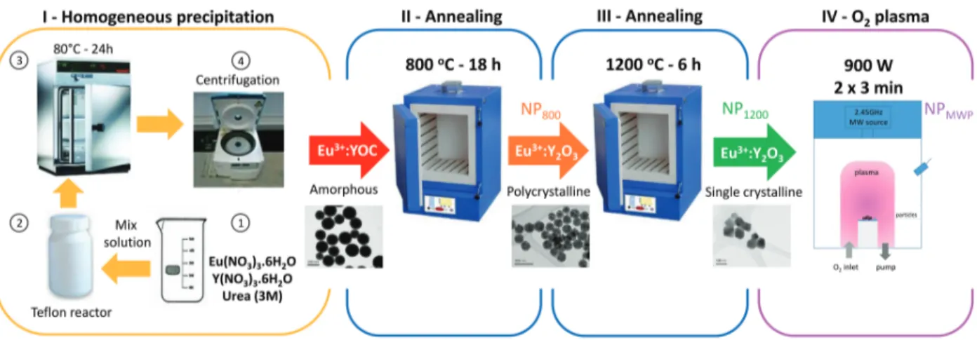
A novel strategy combining chemical synthesis, high-temperature annealing and high-power microwave oxygen plasma processing is here presented to obtain single crystalline Eu3+:Y
2O3
NPs (0.3% at.) with improved optical T2 for nanoscale optical quantum technologies. The
full procedure is displayed in Figure 1: Amorphous Y(OH)CO3 · n H2O:Eu3+ precursor
NPs (YOC:Eu3+) are synthesized by homogeneous precipitation (see Methods)24.
Well-dispersed polycrystalline Eu3+:Y
2O3 NPs (0.3%at.) are obtained after annealing for 18 h
at 800 ◦C. A second annealing follows at 1200 ◦C for 6 h. This step yields single crystalline
under oxygen plasma for two times 3 minutes with a MW excitation power of 900 W. Under these conditions, the sample reaches a temperature of approximately 500 ◦C, evidenced by
glowing, and a consistent improvement of the NPs optical coherence properties is observed. For clarity, once annealed, twice annealed and further oxygen plasma treated NPs will be hereinafter identified as NP800, NP1200 and NPMWP respectively.
Figure 1: Schematic representation of the synthesis and post-treatment strategy. The ho-mogeneous precipitation synthesis is here described in four steps: (1) Preparation of the rare-earth nitrates and urea aqueous solutions. (2) Addition of the mixed solution to a teflon reactor. (3) Calcination for 24 h at 85 ◦C. (4) Washing and collection of Eu3+:YOC
NPs. The amorphous Eu3+:YOC NPs are then first annealed for 18 h at 800 ◦C followed by
a second annealing at 1200◦C for 6 h. Both annealing steps are done in air atmosphere. The
twice-annealed NPs are finally treated under pure oxygen plasma for two times 3 minutes at 900 W MW excitation power, reaching a temperature of ∼ 500 ◦C. Refer to the Methods
for more details.
Structural characterizations
Structural and morphological evolutions induced by the different post-synthesis treatments are shown in Figure 2. The NP800 sample presents polycrystalline features and the particle
size follows a log-normal distribution with an average value of 102 ± 17 nm and crystalline domains of 30 ± 10 nm (Figure 2 (b-b2-b3)). In contrast, the NPs structure and mor-phology clearly changes after the second annealing at 1200◦C. Indeed, NP
1200 present single
morphology characterized by plain facets and sharp edges (Figure 2(c)). In addition, we observe that performing two high-temperature annealing steps helps limiting particle ag-gregation with respect to a single annealing treatment at 1200 ◦C for 18 h17. No further
morphological modifications are observed after the oxygen plasma processing (Figure 2 (d-d2)) and the latter does not lead to further particle aggregation either. The average particle size of the final NPMWP is estimated at 100 ± 31 nm (Figure 2 (d3)).
Figure 2: Structural and morphological evolution of the NPs along the different post-treatments shown by TEM. (a) As synthesized Eu3+:YOC NPs. (b) NP
800. (b2) Zoom
on one isolated NP800. (b3) Size distribution for NP800. (c) NP1200. (d) NPMWP. (d2) Zoom
on one isolated NPMWP. (d3) Size distribution for NPMWP.
The NPs transition from polycrystalline to single crystalline is also evidenced by X-ray diffraction (XRD). As displayed in Figure 3, the characteristic diffraction pattern of the Y2O3 cubic phase (Ia-3 space group, JCPDS 01-080-6433) is found in all cases. However,
the peak broadening is remarkably reduced after the second annealing at 1200 ◦C. This
is due to the increase of the crystalline domain size, in full agreement with TEM results. The crystalline domain size, obtained from the diffraction peaks’ full-width half maximum (FWHM) using Scherrer’s equation (see Methods), is found equal to 30 ± 2 nm in NP800,
increasing up to 111 ± 13 nm in NP1200. The average crystalline domain size in NPMWP is
(Figure 2). In conclusion, TEM imaging and XRD diffraction results demonstrate that the synthesis and post-treatment strategy proposed here enables obtaining dispersed single crystalline Y2O3:Eu3+ NPs of ∼100 nm average size.
Figure 3: XRD patterns from NP800, NP1200 and NPMWP. Rhomb symbols indicate the
position of diffraction peaks assigned to a parasitic yttrium oxyfluoride (YOF) rhomboedral phase (JCPDF: 71-2100) due to a pollution from the plasma experimental equipment. The amount of this phase is estimated at 3-5%. Curves are vertically shifted for clarity.
High-resolution and coherent optical spectroscopy of Eu
3+in Y
2O
3NPs
High-resolution optical spectroscopy techniques are highly sensitive, providing insight into modifications in the RE ions environment. They are particularly useful when those changes are minor, therefore unnoticeable by most characterization techniques. For instance, im-portant information can be extracted from the study of the RE’s optical inhomogeneous lines (Γinh). At low temperatures, the RE transitions are inhomogeneously broadened due
strain induced by defects, with broadenings ranging from hundreds of MHz to hundreds of GHz25. These defects include the RE dopants themselves, but also other uncontrolled
impurities. Therefore, the analysis of transition linewidths and lineshapes provides insight into the amount and nature of defects in the material26,27. Another spectroscopic parameter
QT applications is the optical coherence lifetime T2. Indeed, T2 is extremely sensitive to
dynamic perturbations such as electric or magnetic field fluctuations or dynamical disorder modes (TLS)16. In the following, we study the 7F
0 ↔5D0 transition of Eu3+ at 580.883 nm
(vac.), corresponding to Eu3+ ions at the C
2 symmetry site24, and we compare
inhomoge-neous linewidths and T2 results from NP1200 and NPMWP samples.
Figure 4: (a) Experimental setup. AOM stands for acousto-optic modulator, PBS for polar-ising beam splitter, APD for avalanche photodiode and L and M represent lenses and mirrors. (b) Γinh for the 7F0 →5D0 Eu3+ transition in NP1200 and NPMWP samples. Γinh values are
estimated by Lorentzian fit. The optical transition frequency at 0 detuning corresponds to 516.0979 ± 0.0002 THz (580.8830 ± 0.0001 nm in vac.) for NP1200, and 516.0992 ± 0.0002
THz (580.8815 ± 0.0001 nm in vac.) for NPMWP. (c) Photon echo decays from NP1200 and
NPMWP samples. T2 values are derived by single exponential fit to the photon echo decay
data (see Methods). (d) T2 as a function of excitation frequency for NP1200 (green) and
NPMWP (red).
A schematic representation of the experimental setup used in these measurements is shown in Figure 4(a). For a more detailed description refer to the Methods section. Inho-mogeneous linewidths measured at 12 K are displayed in Figure 4(b). Both lines present Lorentzian lineshape, indicating that the broadening originates from point defects26. In
par-ticular, a FWHM of 11 GHz is obtained from the NP1200 sample, equivalent to 0.0124 nm
(or 0.37 cm−1). This is similar to values reported in Eu3+:Y
2O3 transparent ceramics21 and
larger NPs17,24. With an Eu3+ concentration of 0.3%at., the contribution to Γ
inh from Eu3+
ions is estimated at 6 GHz by comparison to high-quality single crystals28. Therefore, an
additional broadening of 5 GHz is observed, revealing the presence of additional defects or impurities. This contribution is clearly larger in the NPMWP case, with Γinh reaching 27
GHz. Thus, new point defects are created due to the MW-excited oxygen plasma action. In addition, the inhomogeneous line center is blueshifted of ∼1 GHz in the NPMWP sample,
pointing that the oxygen plasma processing induces compressive strain in the lattice27.
Interestingly, the optical coherence lifetime of Eu3+, measured at 1.4 K using the
two-pulse photon echo technique16 (see Methods for more details), is significantly improved by
the MW oxygen plasma treatment. As displayed in Figure 4(c), a T2 of 5.7±0.2 µs is
measured in the NPMWP sample. This is about 3 times longer than in the NP1200 sample
(T2 = 1.91±0.04 µs). Furthermore, this improvement is not limited to ions absorbing at the
central wavelength. Instead, it is observed along the whole inhomogeneous absorption line with an enhancement factor varying between 3 and 5 (Figure 4(d)). This result indicates that the oxygen plasma treatment acts on all ions, and it is not limited to e.g. Eu3+ ions
close to surface. For the latter, transition frequencies are indeed expected to be shifted from the line center. We note that the maximum T2 obtained here is longer than that observed
in 5 µm size particles containing 60 nm nanocrystals synthesized by solvothermal method (T2 = 3.7 µs)29, and it is comparable to values reported in 400 nm size NPs (T2 = 7 µs)16
and some bulk single crystals28. In addition, the enhancement effect is not limited to these
particular NPs as optical T2 enhancement by oxygen plasma has also been recently observed
in chemically etched Eu3+:Y
2O3NPs17 as well as Pr3+:Y2O3NPs of different sizes19.
We investigated the effect on T2 of varying different plasma parameters, such as nature
and pressure of the forming gases and treatment duration time. (Figure 5). By this, we conclude that coherence lifetimes are only improved when the plasma forming gases contain
Figure 5: (a) Photon echo decays of Eu3+:Y
2O3 NPs treated two times for 3 minutes under
different plasma conditions. A batch of 400-nm-diameter NPs was used in this study (see Methods for more details) (b) T2 and Γinh evolution as a function of plasma duration time.
The longest T2 is obtained for a plama duration of 3 minutes. Further optimization revealed
the optimum sequence of two times 3 minutes applied elsewhere. A batch of 140-nm-diameter NPs was used in this study (see Methods for more details).
oxygen, and that the enhancement effect increases when increasing the oxygen content. In contrast, a pure argon gas flow exhibited no impact (Figure 5(a)). A control experiment in which the particles were treated under high-power MW radiation at atmospheric pressure (i.e. no plasma) was also carried out, showing no effect. The impact of the plasma duration time on T2 and Γinh is given in Figure 5(b). When tuning the oxygen plasma duration time
from 1 to 5 minutes, T2 is observed to first increase and then decrease, yielding the longest
T2 or larger improvement factor, for a treatment duration of 3 minutes. At the same time,
a monotone inhomogeneous linewidth increase is obtained when increasing the treatment duration time. In summary, we find a clear correlation between the presence of oxygen in the plasma forming gases and the increase of optical T2 in the NPs. The enhancement effect,
of a factor 3-5, is consistently observed in all ions (Figure 4(d)), and also for different batches of NPs (Figure 5)17,19. In parallel, the MW oxygen plasma treatment induces
a broadening of the optical inhomogeneous line, indicating and increased number of point defects.
FT-IR, luminescence and EPR characterizations
A series of optical and magnetic characterizations were performed on NP1200 and NPMWP
samples, before and after MW oxygen plasma treatment, to gain understanding about the mechanisms behind the observed T2enhancement and Γinhbroadening. Those include Fourier
transform infrared spectroscopy (FT-IR), time-resolved photoluminescence (PL), cathodo-luminescence (CL) and electron paramagnetic resonance (EPR).
Figure 6 shows the evolution of FT-IR spectra from the Eu3+: YOC precursor through
the subsequent treatments. The Eu3+:YOC spectrum is characterized by strong absorption
signals in the 1400-1500 cm−1 and 3000-3400 cm−1 regions, corresponding to C-O and O-H
bond vibrations30. The Y
2O3 phase formed after annealing at 800 ◦C is confirmed by the
appearance of Y-O bonds31 at 565 cm−1. However, C-O and O-H vibration bands are still
carbonates are expected to be removed and these bands show no clear evolution from NP1200
to NPMWP, we conclude that they are due to surface-adsorbed molecules from ambient
atmosphere32. Therefore, they seem to play no role in the observed T
2 increase and Γinh
broadening after oxygen plasma processing.
Figure 6: FT-IR spectra of Eu3+:YOC precursor NPs, NP
800, NP1200 and NPMWP. Curves
are vertically shifted for clarity.
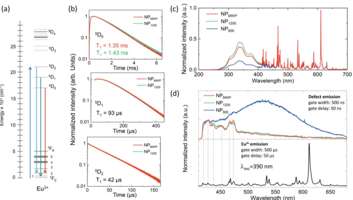
In addition, no fluorescence lifetime variations were observed between NP1200and NPMWP
samples. This was evidenced by measuring the fluorescence lifetimes (T1) of the 5D0, 5D1
and 5D
2 excited state levels (Figure 7(a)). Those were recorded from the Eu3+ emissions
at 611 nm (5D
0 → 7F2), 535 nm (5D1 → 7F1), and 516 nm (5D2 → 7F2), under pulsed
excitation at 465 nm (7F
0 →5D2), yielding T1 values of 1.35 ms, 95 µs and 42 µs respectively
(Figure 7(b)). In contrast, cathodoluminescence spectra display clear differences with the applied treatments (Figure 7(c)). All samples show the characteristic Eu3+ emissions in
the 400-700 nm range, corresponding to the 5D
J (J = 0 ,1 ,2 ,3) → 7FJ (J = 0, 1, 2, 3, 4)
transitions. Additionally, a broadband emission in the 250-400 nm range is observed. After being normalized to the Eu3+ 5D
0 → 7F2 transition at 611 nm, the intensity of this broad
emission is observed to increase in the NP1200sample and then, to slightly decrease after MW
and has been observed in annealed Eu3+:Y
2O3 thin films34. Based on these previous works,
we attribute this broad emission to native defects in Y2O3 35,36. In particular, this band has
been assigned to oxygen interstitials (Oi)33, resulting from oxygen diffusion into the NPs. In
contrast, no evidence of Eu2+ emission has been observed33.
Figure 7: (a) Eu3+energy level diagram indicating the investigated transitions. (b) PL decays
from NP1200 and NPMWP samples. The population lifetime T1 is measured by monitoring
the 611 nm (5D
0 → 7F2), 535 nm (5D1 → 7F1), and 516 nm (5D2 → 7F2) emissions under
pulsed excitation at 465 nm (7F
0 → 5D2). (c) CL spectra normalized to the 611 nm Eu3+
emission peak. (d) Time-resolved PL spectra under 390 nm excitation for two different time gates. Fast emissions from defects are evidenced by the short-time detection window from 50 ns to 550 ns (upper panel), while the regular 4f-4f Eu3+ transitions dominate the emission
spectrum for detection between 50 µs and 550 µs (lower panel).
To gain further insight into defect types and their concentration in the NPs, time-resolved PL and EPR studies were also performed. As illustrated in Figure 7(d), different PL spec-tra are obtained from the NPs depending on the applied treatments when using a gated detection. This technique enables separating short-lived emissions like those coming from defects (Figure 7(d), upper panel), from longer-lived ones, in this case, the Eu3+ 4f-4f
observed in the 400-650 nm range for the NP800 sample. A similar short-lived broadband
has been previously observed in Eu3+:Y
2O3 transparent ceramics21 and Y2O3 thin films37,
and attributed to neutral oxygen vacancies (VO)
21,38. After the second annealing at 1200 ◦C (NP
1200), this broad emission band weakens, becoming indistinguishable from the
back-ground. Indeed, only 4f-4f emissions from Eu3+ions can be indentified between 400 and 500
nm in NP1200 and NPMWP samples under the same recording conditions. Therefore, no
dif-ference could be detected before and after MW oxygen plasma processing by this technique. In contrast, electron paramagnetic resonance (EPR) provides interesting results.
EPR investigations were carried out at 4.5 K, 20 K, 70 K and 100 K respectively. Figure 8 shows normalized spectra from NP1200 and NPMWP samples. Two resonance lines at 335.1
mT (line I) and 341.3 mT (line II) can be observed in both cases, corresponding to g = 2.004 and g = 1.967 respectively. Similar EPR signals have been previously observed in Y2O321,39–41. Accordingly, the lines in Figure 8 were attributed to interstitial superoxide
anions O−
2 (line I), and charged oxygen vacancies V +
O (line II) i.e. an oxygen vacancy center
with a trapped electron. These two lines show different temperature dependences. In par-ticular, the O−
2 EPR signal saturates at low temperatures while the intensity of the V+O peak
increases. Furthermore, it is observed that the O−
2 signals are of similar intensities before
and after MW oxygen plasma processing while the V+
O signal is clearly stronger afterwards,
indicating an increase of this type of defect. The EPR spectrum of Eu3+:Y
2O3NPs after
800 ◦C annealing was also measured (Figure 10), revealing the presence of O−
2 and V+O
centers. However, both appeared as very weak signals at this stage. It is worth noting that the evolution of the O−
2 centers in EPR is very similar to that of the CL broadband emission
(Figure 7 (c)), attributed to interstitial oxygen centers (Oi). We note too that no EPR
signals from Eu2+ ions were detected, in agreement with CL results (Figure 7(c)).
In conclusion, from CL, PL and EPR characterizations, we demonstrate the ability of the high-temperature annealing and MW oxygen plasma post-synthesis treatments to modify the oxygen-related native defects in the NPs. Those are already modified between the first
Figure 8: EPR spectra NP1200 and NPMWP samples recorded at different temperatures. Two
signals are identified, referred to as I and II, corresponding to interstitial superoxide anions (O−
2) and charged oxygen vacancies (V+O) respectively.
annealing at 800 ◦C and the second annealing at 1200 ◦C, with the observed increase of
interstitial O−
2 (Figure 7(c)) and the reduction of the number of neutral oxygen vacancies
(VO) (Figure 7(d)). Interestingly, a more specific effect was revealed by EPR: the increase
in the number of charged oxygen vacancies (V+
O) following the MW oxygen plasma processing.
Discussion
Oxygen vacancies and oxygen interstitials are point defects abundantly found in oxide ma-trices, and in particular, in Y2O3 35,36. Among the vacancies, we often distinguish between
neutral (VO) and charged (V+O) oxygen vacancies, also referred to as F and F+ centers in
lit-erature respectively38. Neutral vacancies have two trapped electrons, therefore same charge
as the missing oxygen anion, while charged vacancies have a single trapped electron. Doubly-charged vacancies or V++
O i.e. without any trapped electron, can also be found (Figure 9).
and if they are present in radical form (O) or in molecular form (O2). The presence and
rela-tive amounts of all these defects can strongly vary depending on the synthesis conditions, and on the different post-treatments applied to the material, impacting its structural, electrical and transport properties35,42,43. As an example, the presence of oxygen vacancies modifies
the dielectric properties of oxyde materials35,44 and contribute to electric conduction45.
Ac-cording to the present study, they could also be playing a major role in the optical dephasing mechanisms in Eu3+:Y
2O3 NPs, leading to T2 shortening i.e. homogeneous linewidth (Γh)
broadening, with the two related by Γh=(πT2)−1. For Eu3+ ions in Y2O3NPs, Γh depends
on several contributions defined as16:
Γh = Γpop+ ΓTemp+ Γmagnetic+ Γelectric (1)
Γpop represents line broadening related to the excited-state population lifetime,
calcu-lated as Γpop=(2πT1)−1. ΓTemp refers to temperature-dependent dephasing mechanisms. In
the particular case of Eu3+:Y
2O3 NPs, at 1.4 K, those are mostly due to two-level systems
(TLS) related to residual disorder, resulting in a linear temperature dependence16. Γ magnetic
stands for ion-spin and spin-spin magnetic interactions. Finally, by Γelectric we refer to line
broadening induced by fluctuating electric fields. This term is usually neglected in bulk single crystal while it is a major contribution in NPs. Indeed, the three first contributions in Eq. 1 are largely insufficient to explain the measured optical homogeneous linewidth of 45 kHz in 400-nm-diameter Eu3+:Y
2O3 NPs16. A plausible source of electric noise in nanomaterials
is the surface. Indeed, surface states are very often blamed for both electric and magnetic perturbations resulting in T2 decrease in nanomaterials46. Besides the surface, the native
point defects constitute another possible source of electric noise. In particular, phenomena like charge tunneling between charged oxygen vacancies can induce electric field fluctuations in the Eu3+ ions environment, reducing T
In the present work we have shown that both high-temperature annealing and MW oxy-gen plasma treatments result in oxyoxy-gen diffusion into the NPs leading to oxyoxy-gen vacancy recombination and oxygen excess. However, the mechanisms involved are not strictly equiv-alent for these two treatments. In the annealing case, O diffusion must be preceded by O2
adsorption to the NPs surface and then dissociation. This mechanism is enhanced by the annealing temperature as demonstrated by the reduction of the oxygen vacancies from NP800
to NP1200 (Figure 7 (d)). We note that T2 must be very short in the NP800sample as photon
echoes cannot be detected while microsecond-long T2 is obtained in NP1200 (Table 1). This
can be related to the observed oxygen vacancies reduction, but also to other mechanisms. In particular, the crystalline domain size is largely increased from 30 nm to ∼110 nm by the second annealing. The impact of the crystalline domain size on T2 has been suggested in
previous investigations, indicating that T2 increases when the surface to volume ratio at the
crystalline domain level decreases17–19. In contrast, a direct correlation between oxygen
dif-fusion, defects modification and enhanced T2 is observed in the oxygen plasma case. For this
post-treatment, the diffusion process is more efficient as radical oxygen atoms are already present in the plasma (Figure 11). Therefore, those can directly diffuse inside the material after adsorption at the surface. Moreover, the high temperature reached by the NPs during the treatment (500 ◦C) is probably enhancing this diffusion. As a result, the optical T
2 is
increased of a factor 3-5 by few minutes of oxygen plasma treatment while no improvement is observed when further increasing the annealing time before plasma processing.
Table 1: Summary of results from NP1200 and NPMWP samples.
Parameter NP1200 NPMWP
Particle size (nm) 100±31 100±31 Crystalline domain size (nm) 111±13 121±15 Γinh (GHz) 11±1 27 ±1
T1 (ms) 1.43 1.35
T2 (µs) 1.91±0.04 5.67±0.21
The increase in charged oxygen vacancies (V+
O), revealed by EPR, is a very interesting
specific effect associated to the MW oxygen plasma processing. It provides a deeper in-sight into the complex dephasing mechanisms taking place in the NPs and how the oxygen diffusion induced by this treatment counteracts them. Based on the present results, we propose that electric noise originates from charge tunneling between neighboring VO and
V+
O centers. Oxygen deficiency conditions can lead to such pairs in the crystalline matrix,
their removal being responsible for the observed T2 improvement after oxygen plasma. Two
possible reactions between a diffusing O atom and a (VO - V+O) pair can be foreseen:
• (VO + V+O) + O → OO + V+O • (VO + V+O) + O → 2V + O + O − i
where OO represents a recombined oxygen anion at a regular lattice site and O−i a
negatively-charged interstitial oxygen atom. The result of these reactions is consistent with the observed experimental results as they yield to O−
i increase, overall reduction of the
number of oxygen vacancies, and relative increase of the V+
O/VO ratio (Figure 8). More
importantly, these two reactions erase the (VO - V+O) tunneling pairs, proposed as source
of electric noise. As a drawback, an excess of V+
O and O −
i can be also detrimental to the
optical coherence lifetime for example by increasing disorder and TLS effect. Therefore, it is observed that T2 decreases as the oxygen plasma treatment overcomes a given time
du-ration (Figure 5(b)). The increased amount of interstitials following the oxygen plasma treatment can also explain the observed inhomogeneous linewidth broadening (Figure 5(b)) and induced compressive strain in the lattice (line blueshift). Further optimization of the parameters involved in the plasma creation as the MW power and the oxygen pressure would be required to favor VO recombination (first reaction) while limiting V+O and oxygen excess
in the lattice (second reaction).
post-particles in small mode volume, high-finesse fiber cavities. Moreover, single crystalline par-ticles maximize, for a given size, the number of ions that can interact with electric and magnetic fields, including light, in the same way. This is important for accurate control of optical and spin quantum states e.g. in scalable processors or memories.18 Single crystalline
particles are achieved thanks to the two-step high temperature annealing. It cannot be ob-tained by the MW oxygen plasma treatment alone, which does not change the NPs structure nor morphology (Figures 2 and 3). It is however necessary to increase the coherence life-times obtained after the two-step annealing. In conclusion, both high-temperature annealing and MW oxygen plasma treatments provide important advantages and have to be combined to obtain optimized RE NPs for QT. More generally, this process, and in particular the high power oxygen plasma treatment, could be applied to other oxide matrices to reduce/tune oxygen vacancies and related defects, which can limit material performance in a broad range of applications in photonics and electronics.
Conclusion
We have demonstrated a novel strategy combining a two-step high-temperature annealing in air and a microwave-excited oxygen plasma processing in the synthesis and optimization of Eu3+:Y
2O3nanoparticles of 100 nm size. We performed complete structural investigations
on such NPs and showed a progression from polycrystalline to single crystalline objects with-out substantial particle-aggregation under high-temperature annealing up to 1200◦C. More
importantly, T2 extension up to a factor 5 was successfully achieved by the oxygen plasma
treatment. These promising results confirm nanoscale Eu3+:Y
2O3 NPs as very appealing
can-didates for quantum information storage and processing. We conclude that the microwave-excited oxygen plasma treatment efficiently tunes oxygen-related defects and decreases the electric noise in the NPs. In particular, we propose that it reduces charge tunneling between close-lying oxygen vacancies. Since these non-stoichiometric defects are common in oxides,
such defect engineering could be potentially applied to other RE oxide materials to fine-tune the local environments and charge variations around the RE ions. Thus, this could enable to achieve desirable, electrical, luminescence and/or optical coherence properties for a wealth of applications.
Methods
Eu3+:YOC nanoparticles synthesis. 0.3 at.% Eu3+:YOC NPs were synthesized by
ho-mogeneous precipitation from aqueous solutions of yttrium nitrate Y(NO3)3· 6 H2O (99.99
% pure, Alfa Aesar), europium nitrate Eu(NO3)3· 6 H2O (99.999 % pure, Alfa Aesar) and
urea CO(NH2)2 (> 99 % pure, Sigma), with metal and urea concentrations of 7.5 mmol
L−1 and 3 mol L−1 respectively. The mixed solution was heated at 85 ◦C for 24 h in a
teflon reactor, leading to the precipitation of Eu3+:Y(OH)CO
3 · n H2O (Eu3+:YOC) NPs.
Once cooled down to room temperature, the NPs were washed once with distilled water and twice with absolute ethanol to remove synthesis byproducts. Every washing was followed by centrifugation at 13000 rpm and 4 ◦C. Finally, Eu3+:YOC NPs of 140 nm average size were
collected in the form of white powders after drying at 80 ◦C for 24 h.
High-temperature annealing treatment. A two-step annealing process is proposed in this work, which allows for high temperature treatment of small NPs (< 150 nm) without significant particle aggregation. The first annealing is performed at 800 ◦C for 18 h, with
a heating rate of 5 ◦C min−1, to transform the Eu3+:YOC precursor into Eu3+:Y
2O3 phase
(JCPDS 01-080-6433). The resulting Y2O3NPs are polycrystalline, with 100-nm-diameter
average size. We note that size reduction with respect to the as-synthesized Eu3+:YOC NPs
is expected24. Then, a second annealing treatment is applied at 1200 ◦C for 6 h, with a
heating rate of 3 ◦C min−1, to obtain dispersed single crystalline nanoparticles. Treatment
improve-ment is observed for longer treatimprove-ments, and higher temperatures than 1200◦C lead to severe
particle aggregation. After each treatment, the powders are ground to break the soft aggre-gates. The cooling rate was set to 5 ◦C min−1 in both cases.
Microwave oxygen plasma processing. A MW oxygen plasma treatment was applied to the Eu3+:Y
2O3 NPs after the two-step annealing process. For this, the Eu3+: Y2O3
powders are spread onto a glass slide and introduced into a home-made plasma chamber. The chamber consists of a MW cavity in which a 2.45 GHz standard microwave source can deliver 900 W. A vacuum sealed quartz bell jar was pumped down to 10−2 mbar before being
flushed with a 10 sccm pure O2 flow for a few minutes. The pressure was then set to 0.5-1
mbar by regulating the pumping speed with a butterfly valve (Figure 12). As soon as the microwave excitation was switched on, the O2 plasma lit up in the low pressure region of the
bell jar. For the standard optimized treatment, the plasma was sustained for 3 minutes, then the system was left to cool down for a few minutes before the plasma was switched on once again for another 3 minutes. The chamber was eventually vented to atmospheric pressure and the treated nanoparticles collected for further structural and spectroscopic characterizations. To investigate the influence of the oxygen plasma on the NPs properties, several atmo-spheres and plasma duration times were tested. In particular, pure Ar gases and 50 % Ar: 50% O2 mixed gases were tested under the same plasma conditions and the plasma duration
time was varied from 1-5 minutes. These optimization studies were done with two different batches of 0.3%at. Eu3+:Y
2O3 NPs: one with 394±40 nm average size, and one with 140
± 45 nm average size. These two batches were also produced following the route described above, with the exception of a lower urea content (0.3 mol L−1) for the first batch, yielding
larger size particles24, and a single annealing treatment at 1200 ◦C for 6 h in both cases. All
other studies presented in the manuscript were carried out in the same batch of NPs (100 nm size), produced with the fully optimized procedure, i.e. annealed two times, and treated under O2 plasma for 2 times 3 minutes.
Structural characterizations. Morphology, size and dispersion of the NPs were ob-served by scanning electron microscopy (SEM, Zeiss Leo1530) and transmission electron microscopy (TEM, JEOL-JEM-100CX I operating at 100 kV). Particle size and distribution were calculated by Image J software based on at least 100 nanoparticles from different TEM images, assuming that all NPs had spherical shapes. X-ray diffraction (XRD) measurements were performed on a Panalytical XPert Pro diffractometer using monochromatic CuKα1 ra-diation (λ=154.060 pm), in the 2θ range between 12◦ and 150◦, with a step size of 0.0065◦.
Crystalline domain sizes were deduced from diffraction peaks at 20.51◦, 29.16◦, 48.54◦ and
71.06◦ by Scherrer equation:
D = Kλ
βcos(θ) (2)
where D is the crystalline domain size, β is the peak broadening at FWHM corrected by the instrumental response, λ is the CuKα radiation wavelength, K is the shape factor, here set
to 0.89, and θ the Bragg diffraction angle.
Low-temperature high-resolution and coherent spectroscopy. High-resolution and coherent spectroscopy investigations at low temperature were carried out on Eu3+ ions
located at the Y3+ C
2 symmetry site of Y2O3. The powders were placed in a brass holder
between two glass plates forming a layer with a thickness of 500 µm. Cryogenic conditions were provided by a He bath cryostat (Janis SVT-200), operated in liquid and gas modes. The sample temperature was controlled with a Si diode (Lakeshore DT-670) attached to the sample holder. Inhomogenenous linewidths for the 7F
0 →5D0 transition of Eu3+ ions were
recorded at 12 K by monitoring the5D
0 →7F2 fluorescence while scanning a CW
frequency-stabilized ring dye laser (Sirah Matisse DS, 300 kHz linewidth) pumped by a Coherent Verdi G10 laser. A long-pass filter (590 nm cut-off wavelength) was placed in front of the detector (APD Thorlabs 110 A/M) to reject the excitation light. Optical T2 values were
For this, pulsed sequences were created by modulating the CW laser output with an acousto-optic modulator (AA Opto Electronic MT200-A0.5,VIS) driven by an arbitrary waveform generator (Agilent N8242A). Scattered light transmitted through the powders was collected and then focussed by a series of large-diameter lenses on the APD detector (Figure 4(a)). The length of the exciting and rephasing pulses in the sequence was set to 1 and 1.5 µs respectively and their power to ∼ 300 mW (Figure 13). The decay of the photon echo amplitude follows:
Aecho = A0e
−2τ
T2 (3)
where τ = 0 is the time delay between the first and second pulse in the sequence, and A0
is the echo amplitude at τ = 0. T2 values were derived from experimental echo decay data
by single exponential fit. Homogeneous linewidths (Γh) were then determined as Γh=(πT2)−1.
Optical spectroscopy and defect characterizations. FT-IR studies were performed in transmission mode between 400 and 4000 cm−1 with a Bruker Tensor 27 spectrometer.
Samples were prepared for measurements using the conventional KBr pellet method. Pho-toluminescence (PL) spectra were obtained at room temperature under 390 nm excitation by a tunable optical parametric oscillator (OPO) pumped by a Nd3+ YAG Q-switched laser
(Ekspla NT342B-SH with 6 ns pulse length and 10 Hz repetition rate). The spectra were recorded by a spectrometer (Acton SP2300) equipped with 300 grooves/mm holographic grating and an ICCD camera (Princeton Instruments). A time-gated detection was carried out to separate emissions from Eu3+ ions (500 µs gate width starting after 50 µs) and from
defect centers (500 ns gate width starting at 50 ns). Decay measurements were recorded using the same setup except for a photomultiplier tube detector. Decay curves for the 5D
0, 5D
1 and 5D2 energy levels of Eu3+ ions were recorded at 611, 535 and 516 nm respectively
with an excitation wavelength of 465 nm. Decay data were recorded with a digital oscil-loscope. Cathodoluminescence (CL) measurements were performed by a SEM (Zeiss EVO MA15) equipped with a Horiba HCLUE CL system. The electron gun was operated with an
accelerating voltage of 10 kV and a probe current of 10 nA. Light emitted in the UV-visible range by the NPs was collected by a motorized and retractable curved mirror and sent to a spectrometer HORIBA TRIAX 500 equipped with a 600 grooves/mm grating and a slit size of 100 µm to disperse the light onto a Pelletier cooled CCD camera. Electron paramagnetic resonance (EPR) measurements were performed using a Bruker Elexsys E500 spectrometer and a Super-high-sensitivity probehead in X-band (∼9.5 GHz). EPR spectra were recorded with a microwave power of 10 mW.
Acknowledgement
Shuping Liu and Alexandre Fossati contributed equally. This project has received funding from the European Union Horizon 2020 Research and Innovation Programme under grant agreement no. 712721 (NanOQTech). S. Liu is supported by the Key R&D Program of Guangdong province (Grant No. 2018B030325001). We thank Patricia Beaunier for her help with TEM measurements and Nadia Touati for assistance during EPR experiments.
Supporting Information Available
Figure 9: Schematic representation of the types of oxygen vacancies in Y2O3.
Figure 10: EPR spectra taken at various temperatures before and after O2 plasma
treat-ment. The MW O2 plasma treatment was here applied immediately after the 800 ◦C
an-nealing, skipping the 1200 ◦C step. These measurements were done on a different batch of
Eu3+:Y
2O3NPs, with 60 nm average size, obtained by a modified homogeneous precipitation
route.
Figure 11: Optical emission spectrum of a pure O2 plasma used to treat Eu3+:Y2O3 NPs.
Figure 12: Schematics of the MW plasma apparatus and picture of the chamber during O2
plasma generation.
Figure 13: Two-pulse photon echo sequence (upper) and optical coherence phase evolution represented at the Bloch sphere (lower). The optical coherence lifetime is evaluated by monitoring the decay of the photon echo amplitude when increasing the time delay τ between the excitation pulse (π/2) and the rephasing pulse (π).
References
1. Acín, A.; Bloch, I.; Buhrman, H.; Calarco, T.; Eichler, C.; Eisert, J.; Esteve, D.; Gisin, N.; Glaser, S. J.; Jelezko, F. et al. The quantum technologies roadmap: a Euro-pean community view. New J. Phys. 2018, 20, 080201.
2. Goldner, P.; Ferrier, A.; Guillot-Noël, O. In Handbook on the Physics and Chemistry of Rare Earths; Bünzli, J.-C. G., Pecharsky, V. K., Eds.; Elsevier: Amsterdam, 2015; pp 1–78.
3. Achard, J.; Jacques, V.; Tallaire, A. CVD diamond single crystals with NV centres: a review of material synthesis and technology for quantum sensing applications. J. Phys. D: Appl. Phys. 2020, 1–43.
4. Atatüre, M.; Englund, D.; Vamivakas, N.; Lee, S.-Y.; Wrachtrup, J. Material platforms for spin-based photonic quantum technologies. Nat. Rev. Mater. 2018, 3, 1–14.
5. Equall, R. W.; Cone, R. L.; Macfarlane, R. M. Homogeneous broadening and hyperfine structure of optical transitions in Pr3+: Y
2SiO5. Physical Review B 1995, 52, 3963–3969.
6. Arcangeli, A.; Lovrić, M.; Tumino, B.; Ferrier, A.; Goldner, P. Spectroscopy and coher-ence lifetime extension of hyperfine transitions in 151Eu3+:Y
2SiO5. Phys. Rev. B 2014,
89, 184305.
7. Zhong, M.; Hedges, M. P.; Ahlefeldt, R. L.; Bartholomew, J. G.; Beavan, S. E.; Wit-tig, S. M.; Longdell, J. J.; Sellars, M. J. Optically addressable nuclear spins in a solid with a six-hour coherence time. Nature 2015, 517, 177.
8. Businger, M.; Tiranov, A.; Kaczmarek, K. T.; Welinski, S.; Zhang, Z.; Ferrier, A.; Gold-ner, P.; Afzelius, M. Optical Spin-Wave Storage in a Solid-State Hybridized Electron-Nuclear Spin Ensemble. Phys. Rev. Lett. 2020, 124, 053606.
9. Puigibert, M. l. G.; Askarani, M. F.; Davidson, J. H.; Verma, V. B.; Shaw, M. D.; Nam, S. W.; Lutz, T.; Amaral, G. C.; Oblak, D.; Tittel, W. Entanglement and nonlocal-ity between disparate solid-state quantum memories mediated by photons. Phys. Rev. Research 2020, 2, 013039.
10. Bussières, F.; Clausen, C.; Tiranov, A.; Korzh, B.; Verma, V. B.; Nam, S. W.; Marsili, F.; Ferrier, A.; Goldner, P.; Herrmann, H. et al. Quantum teleportation from a telecom-wavelength photon to a solid-state quantum memory. Nature Photonics 2014, 8, 775. 11. Zhong, T.; Kindem, J. M.; Bartholomew, J. G.; Rochman, J.; Craiciu, I.; Miyazono, E.;
Bettinelli, M.; Cavalli, E.; Verma, V.; Nam, S. W. et al. Nanophotonic rare-earth quan-tum memory with optically controlled retrieval. Science 2017,
12. Dibos, A. M.; Raha, M.; Phenicie, C. M.; Thompson, J. D. Atomic Source of Single Photons in the Telecom Band. Phys. Rev. Lett. 2018, 120, 243601.
13. Bernardo, C.; Julia, B.; Thomas, H.; Franziska, O.; Karmel de Oliveira, L.; Theodor, W. H.; Alban, F.; Philippe, G.; Hugues de, R.; David, H. Cavity-enhanced spectroscopy of a few-ion ensemble in Eu3+:Y
2O3. New Journal of Physics 2018, 20,
095006.
14. Zhong, T.; Goldner, P. Emerging rare-earth doped material platforms for quantum nanophotonics. Nanophotonics 2019, 8, 2003–2015.
15. Schmitt, S.; Gefen, T.; Stürner, F. M.; Unden, T.; Wolff, G.; Müller, C.; Scheuer, J.; Naydenov, B.; Markham, M.; Pezzagna, S. et al. Submillihertz magnetic spectroscopy performed with a nanoscale quantum sensor. Science 2017, 356, 832–837.
16. Bartholomew, J. G.; Lima, K. D.; Ferrier, A.; Goldner, P. Optical Line Width Broadening Mechanisms at the 10 kHz Level in Eu3+:Y
2O3 Nanoparticles. Nano Lett 2017, 17, 778–
17. Liu, S.; Serrano, D.; Fossati, A.; Tallaire, A.; Ferrier, A.; Goldner, P. Controlled size reduction of rare earth doped nanoparticles for optical quantum technologies. RSC Advances 2018, 8, 37098–37104.
18. Serrano, D.; Karlsson, J.; Fossati, A.; Ferrier, A.; Goldner, P. All-optical control of long-lived nuclear spins in rare-earth doped nanoparticles. Nature Communications 2018, 9, 2127.
19. Serrano, D.; Deshmukh, C.; Liu, S.; Tallaire, A.; Ferrier, A.; de Riedmatten, H.; Gold-ner, P. Coherent optical and spin spectroscopy of nanoscale Pr3+:Y
2O3. Physical Review
B 2019, 100, 144304.
20. Macfarlane, R. M.; Shelby, R. M. Sub-kilohertz optical linewidths of the 7F0 ↔ 5D0 transition in Y2O3:Eu3+. Opt. Commun. 1981, 39, 169–171.
21. Kunkel, N.; Bartholomew, J.; Binet, L.; Ikesue, A.; Goldner, P. High-Resolution Optical Line Width Measurements as a Material Characterization Tool. Journal of Physical Chemistry C 2016, 120, 13725–13731.
22. Karlsson, J.; Kunkel, N.; Ikesue, A.; Ferrier, A.; Goldner, P. Nuclear spin coherence properties of 151Eu3+ and 153Eu3+ in a Y2O3 transparent ceramic. J. Phys.: Condens. Matter 2017, 29, 125501.
23. Korner, N.; Beck, E.; Dommann, A.; Onda, N.; Ramm, J. Hydrogen plasma chemical cleaning of metallic substrates and silicon wafers. Surface and Coatings Technology 1995, 76-77, 731 – 737.
24. de Oliveira Lima, K.; Rocha Gonçcalves, R.; Giaume, D.; Ferrier, A.; Goldner, P. Influence of defects on sub-Åoptical linewidths in Eu3+: Y
2O3 particles. Journal of
25. Macfarlane, R. M. High-resolution laser spectroscopy of rare-earth doped insulators: a personal perspective. Journal of Luminescence 100, 1–20.
26. Stoneham, A. M. The theory of the strain broadened line shapes of spin resonance and optical zero phonon lines. Proceedings of the Physical Society 1966, 89, 909.
27. Welinski, S.; Thiel, C. W.; Dajczgewand, J.; Ferrier, A.; Cone, R. L.; Macfarlane, R. M.; Chaneliere, T.; Louchet-Chauvet, A.; Goldner, P. Effects of disorder on optical and electron spin linewidths in Er3+,Sc3+:Y2SiO5. Optical Materials 63, 69–75.
28. Flinn, G. P.; Jang, K. W.; Ganem, J.; Jones, M. L.; Meltzer, R. S.; Macfarlane, R. M. Sample-dependent optical dephasing in bulk crystalline samples of Y2O3:Eu3+. Physical
Review B 1994, 49, 5821–5827.
29. Perrot, A.; Goldner, P.; Giaume, D.; Lovric, M.; Andriamiadamanana, C.; Goncalves, R. R.; Ferrier, A. Narrow optical homogeneous linewidths in rare earth doped nanocrystals. Physical Review Letters 2013, 111, 203601.
30. Tareen, J.; Kutty, T. N.; Krishnamurty, K. Hydrothermal growth of Y2(CO3)3n H2O
(tengerite) single crystals. Journal of Crystal Growth 1980, 49, 761 – 765.
31. Krishna, R. H.; Nagabhushana, B. M.; Nagabhushana, H.; Murthy, N. S.; Sharma, S. C.; Shivakumara, C.; Chakradhar, R. P. S. Effect of Calcination Temperature on Structural, Photoluminescence, and Thermoluminescence Properties of Y2O3:Eu3+ Nanophosphor.
The Journal of Physical Chemistry C 2013, 117, 1915–1924. 32. Som, S.; Sharma, S. K. Eu3+ /Tb3+-codoped Y
2O3nanophosphors: Rietveld refinement,
bandgap and photoluminescence optimization. Journal of Physics D: Applied Physics 2012, 45, 415102.
emission behavior of Y2O3 nanophosphors: A detailed study of structural and optical
properties. Optical Materials 2016, 60, 159–168.
34. Scarafagio, M.; Tallaire, A.; Tielrooij, K.-J.; Cano, D.; Grishin, A.; Chavanne, M.-H.; Koppens, F. H. L.; Armelle, R.; Cassir, M.; Serrano, D. et al. Ultrathin Eu- and Er-Doped Y2O3 Films with Optimized Optical Properties for Quantum Technologies. The
Journal of Physical Chemistry C 2019, 123, 13354–13364.
35. Zheng, J. X.; Ceder, G.; Maxisch, T.; Chim, W. K.; Choi, W. K. Native point defects in yttria and relevance to its use as a high-dielectric-constant gate oxide material: First-principles study. Physical Review B 2006, 73, 104101.
36. Jollet, F.; Noguera, C.; Gautier, M.; Thromat, N.; Duraud, J.-P. Influence of Oxygen Va-cancies on the Electronic Structure of Yttrium Oxide. Journal of the American Ceramic Society 1991, 74, 358–364.
37. Bordun, O. M. Influence of Oxygen Vacancies on the Luminescence Spectra of Y2O3
Thin Films. Journal of Applied Spectroscopy 2002, 69, 430–433.
38. Zorenko, Y.; Zorenko, T.; Voznyak, T.; Mandowski, A.; Xia, Q.; Batentschuk, M.; Friedrich, J. Luminescence of F+and F centers in AI2O3-Y2O3 oxide compounds. IOP
Conference Series: Materials Science and Engineering 2010, 15, 012060.
39. Singh, V.; Rai, V. K.; Ledoux-Rak, I.; Watanabe, S.; Gundu Rao, T. K.; Chubaci, J. F. D.; Badie, L.; Pelle, F.; Ivanova, S. NIR to visible up-conversion, infrared lumines-cence, thermoluminescence and defect centres in Y2O3 : Er phosphor. Journal of Physics
D: Applied Physics 2009, 42, 065104.
40. Santos, S. C.; Rodrigues, O.; Campos, L. L. EPR response of yttria micro rods activated by europium. 2018, 764, 136–141.
41. Costantini, J.-M.; Beuneu, F.; Gourier, D.; Trautmann, C.; Calas, G.; Toulemonde, M. Colour centre production in yttria-stabilized zirconia by swift charged particle irradia-tions. Journal of Physics: Condensed Matter 2004, 16, 3957–3971.
42. Lacroix, B.; Paumier, F.; Gaboriaud, R. J. Crystal defects and related stress in Y2O3
thin films: Origin, modeling, and consequence on the stability of the C-type structure. Physical Review B 2011, 84, 014104.
43. Sarkar, A.; Khan, G. G. The formation and detection techniques of oxygen vacancies in titanium oxide-based nanostructures. Nanoscale 2019, 11, 3414–3444.
44. Cockayne, E. Influence of oxygen vacancies on the dielectric properties of hafnia: First-principles calculations. Phys. Rev. B 2007, 75, 094103.
45. Kevane, C. J. Oxygen Vacancies and Electrical Conduction in Metal Oxides. Phys. Rev. 1964, 133, A1431–A1436.
46. Bluvstein, D.; Zhang, Z.; McLellan, C. A.; Williams, N. R.; Jayich, A. C. B. Extending the Quantum Coherence of a Near-Surface Qubit by Coherently Driving the Paramag-netic Surface Environment. Phys. Rev. Lett. 2019, 123, 146804.