HAL Id: tel-01713283
https://pastel.archives-ouvertes.fr/tel-01713283
Submitted on 20 Feb 2018HAL is a multi-disciplinary open access archive for the deposit and dissemination of sci-entific research documents, whether they are pub-lished or not. The documents may come from teaching and research institutions in France or abroad, or from public or private research centers.
L’archive ouverte pluridisciplinaire HAL, est destinée au dépôt et à la diffusion de documents scientifiques de niveau recherche, publiés ou non, émanant des établissements d’enseignement et de recherche français ou étrangers, des laboratoires publics ou privés.
approach using low temperature PECVD of c-Si(Ge)
Gwenaëlle Hamon
To cite this version:
Gwenaëlle Hamon. III-V/Si tandem solar cells : an inverted metamorphic approach using low temper-ature PECVD of c-Si(Ge). Materials Science [cond-mat.mtrl-sci]. Université Paris Saclay (COmUE), 2018. English. �NNT : 2018SACLX004�. �tel-01713283�
THESE DE DOCTORAT
DE
L’U
NIVERSITE
P
ARIS
-S
ACLAY
PREPAREE A
L’ECOLE POLYTECHNIQUE
E
COLED
OCTORALE N° n°573
Interfaces: Approches interdisciplinaires/fondements, applications et innovation
Spécialité : Physique
Par
Mme Gwénaëlle Hamon
III-V/Si tandem solar cells: an inverted metamorphic approach
using low temperature PECVD of c-Si(Ge) on GaAs
Thèse présentée et soutenue à Palaiseau, le 12 Janvier 2018
Composition du Jury
Prof. Ignacio Rey-Stolle IES - Politécnica de Madrid - Espagne Président du jury
Prof. Eric Tournié IES - Université de Montpellier - France Rapporteur
Prof. Olivier Durand FOTON - INSA Rennes - France Rapporteur
Dr. Bernardette Kunert IMEC - Louvain, Belgique Examinatrice
Dr. Nils-Peter Harder Total GRP - San Jose, Etats-Unis Examinateur
Dr. Stéphane Collin C2N, CNRS, Univ. Paris-Saclay - Marcoussis, France Examinateur
Dr. Julien Penaud Total GRP - Paris La Défense, France Encadrant
Dr Jean Decobert III-V Lab - Nokia Bell Labs - Palaiseau, France Encadrant Prof. Pere Roca i Cabarrocas LPICM, CNRS, Ecole Polytechnique - Palaiseau, France Directeur de thèse
iii
Abstract
Combining silicon with III-V materials represents a promising pathway to overcome the ~29% efficiency limit of a single c-Si solar cell. While the standard approach is to grow III-V materials on Si, this work deals with an innovative way of fabricating tandem solar cells. We use an inverted metamorphic approach in which crystalline silicon or SiGe is directly grown on III-V materials by PECVD. The low temperature of this process (<200 °C) reduces issues due to the difference in thermal expansion coefficient. Also, growing the group IV material on the III-V prevents polarity issues.
The realization of the final tandem solar cell made of SiGe/AlGaAs requires the development and optimization of various building blocks. First, we develop the epitaxy at 175°C of Si(Ge) on (100) Si substrates in an industrial standard RF-PECVD reactor. We prove the promising electrical performances of such grown Si(Ge) by realizing heterojunction solar cells with 1.5 µm epitaxial absorber leading to a Voc up to 0.57 V. We show
that the incorporation of Ge in the layer increases the Jsc from 15.4 up to 16.6 A/cm2 (SiGe25%).
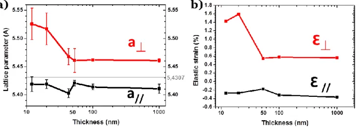
Then, the hetero-epitaxy of Si on GaAs by PECVD is studied. c-Si exhibits excellent structural properties, and the first stages of the growth are investigated by X-ray diffraction with synchrotron beam. We find an unexpected behavior: the grown Si is fully relaxed, but tetragonal. While the GaAs lattice parameter is higher than that of silico, we find a higher out-of-plane Si parameter (a⏊), due to the high hydrogen content in the
layer, but also a smaller in-plane parameter (a//) than the theoretical one. This low a// is probably due to
thermal stress induced by the substrate, and led us to the hypothesis that the temperature during the growth is well above the nominal value. Hereby, we may have found an experimental proof that PECVD growth happens thanks to local heating during the growth.
Meanwhile, we built a know-how in a new technological field in the III-V Lab: photovoltaics. We developed materials for AlGaAs solar cells by MOVPE, as well as their full grid design and process flow in clean rooms. We could reach a high efficiency of 17.6 % for a Al0.22Ga0.78As solar cell, being thus suitable for its integration
in the tandem solar cell. Also, materials to grow tunnel junctions (TJ) were studied, and in particular the n-doping of GaAs with DIPTe precursor to obtain n-doping levels above 2.7x1019 cm-3. While good TJs were
obtained with standard n-doping with Si, Te doping led to TJs with peak tunneling currents up to 3000 A/cm2, reaching state-of-the art. Moreover, by studying the integration of PECVD with III-V materials, we
found that hydrogen plays a strong role in GaAs: its doping level is decreased by one order of magnitude when exposed to a H2 plasma, due to the formation of complexes between H and the dopants (C, Te, Si).
Fortunately, this behavior can be recovered after 3 minutes annealing at 350°C.
Finally, the last step of device fabrication is studied: the bonding on a host substrate. We successfully bonded an inverted AlGaAs cell, removed it from its substrate, and processed a full 2” wafer. We succeeded in growing our first tandem solar cells by growing thick layers (> 1 µm) of Si on inverted AlGaAs solar cells followed by a TJ. Finally, we study the bonding and substrate removal of this final device, being the first tandem solar cell grown by inverted metamorphic growth of Si on III-V.
Keywords: Epitaxy, PECVD, MOVPE, Heteroepitaxy, Tandem Solar Cells, III-V/Si, Tunnel Junctions
Université Paris-Saclay
Espace Technologique / Immeuble Discovery
v
Résumé
La limite théorique d’efficacité d’une cellule solaire simple jonction est de ~29 %. Afin de dépasser cette limite, une des moyens les plus prometteurs est de combiner le silicium avec des matériaux III-V. Alors que la plupart des solutions proposées dans la littérature proposent de faire croître directement le matériau III-V sur substrat silicium, ce travail présente une approche innovante de fabriquer ces cellules solaires tandem. Nous proposons une approche inverse métamorphique, où le silicium cristallin ou SiGe est cru directement sur le matériau III-V par PECVD. La faible température de dépôt (< 200 °C) diminue les problèmes de différence de dilatation thermique, et le fait de croître le matériau IV sur le matériau III-V élimine les problèmes de polarité.
La réalisation de la cellule tandem finale en SiGe/AlGaAs passe par le développement et l’optimisation de plusieurs briques technologiques. Tout d’abord, nous développons l’épitaxie à 175 °C de Si(Ge) sur des substrats de Si (100) dans un réacteur de RF-PECVD industriel. La réalisation de cellules solaires à hétérojonction à partir de ce matériau Si(Ge) crû par PECVD montre que ses performances électriques s’avèrent prometteuses. Nous obtenons pour un absorbeur de 1.5 µm des Voc qui atteignent 0.57 V. L’incorporation de Ge permet d’augmenter le JSC de 15.4 % jusqu’à 16.6 A/cm2 pour Si0.72Ge0.28.
En parallèle, la croissance de cellules solaires AlGaAs a été développée, ainsi que sa fabrication technologique. Nous obtenons une efficacité de 17.6 % pour une cellule simple en Al0.22Ga0.78As. Nous développons aussi des jonctions tunnel, parties essentielles d’une cellule tandem dans une configuration à deux terminaux. Nous développons notamment le dopage n du GaAs en utilisant le précurseur DIPTe, et obtenons des jonctions tunnel ayant des courants pic atteignant jusqu’à 3000 A/cm2, rejoignant ainsi les résultats de l’état de l’art.
Ensuite, nous étudions l’hétéro-épitaxie de Si sur GaAs par PECVD. Le c-Si montre d’excellentes propriétés structurales. Les premiers stades de croissance sont étudiés par diffraction des rayons X avec rayonnement synchrotron. Nous trouvons un comportement inattendu : le Si est relâché dès les premiers nanomètres, mais sa maille est tétragonale. Alors que le GaAs a un paramètre de maille plus grand que le Si, le paramètre hors du plan (a⏊) du Si est plus élevé que son paramètre dans le plan (a//). Nous trouvons une forte corrélation entre cette tétragonalité et la présence d’hydrogène dans la couche de silicium. D’autre part, nous montrons que le plasma d’hydrogène présent lors du dépôt PECVD affecte les propriétés du GaAs : son dopage diminue d’environ un ordre de grandeur lorsque le GaAs est exposé au plasma H2, dû à la formation de complexes entre le H et le dopant (C, Te ou Si). Le dopage initial peut être retrouvé après un recuit à 350 °C. Enfin, nous étudions la dernière étape de fabrication de la cellule tandem : le collage. Nous avons pu reporter une cellule simple inversée en AlGaAs sur un substrat hôte (en Si), retirer le substrat GaAs et effectuer les étapes de microfabrication sur un substrat 2 pouces. Des couches épaisses de Si (>1 µm) ont été crues avec succès sur une cellule AlGaAs inversée suivie d’une jonction tunnel. Le collage de cette cellule tandem, et le processus de fabrication technologique du dispositif final sont ensuite étudiés, afin de pouvoir caractériser électriquement la première cellule solaire tandem fabriquée par croissance inverse métamorphique de Si sur III-V.
Keywords: Epitaxie, PECVD, MOVPE, Heteroepitaxie, Cellules solaires tandem, III-V/Si, Jonctions tunnel
Université Paris-Saclay
Espace Technologique / Immeuble Discovery
vii
Remerciements
En cette fin janvier 2018, il est temps de revenir sur ces trois dernières années qui ont mené à la rédaction de ce manuscrit que, cher lecteur, tu t’apprêtes à lire feuilleter. Je profite de ces quelques paragraphes qui seront probablement les plus lus de ce manuscrit pour exprimer ma plus sincère gratitude aux nombreuses personnes sans qui tout ce travail de thèse n’aurait pas pu voir le jour. La liste de ceux qui m’ont été indispensables à la réalisation de ces travaux est difficile à dresser tellement ils sont nombreux, mais je vais tenter ici de remercier chacun de ceux qui m’ont apporté une aide précieuse lors de ces trois années passées entre les différents laboratoires partenaires. En effet, cette thèse a été effectuée dans le cadre du projet ANR Impetus, qui est le fruit d’une collaboration entre le le LPICM, laboratoire en cotutelle du CNRS et de l’Ecole Polytechnique, le III-V Lab, GIE entre Nokia Bell-Labs, Thales et le CEA Leti, et enfin le GeePs, laboratoire de Supélec. J’ai donc eu l’immense chance de pouvoir avoir accès aux équipements de chacun de ces laboratoires, mais surtout au savoir-faire de leurs membres respectifs. Un tel sujet à la croisée des mondes du silicium et des matériaux III-V, pour applications photovoltaïques requiert la combinaison d’un grand nombre de savoir-faire que je n’aurais pu acquérir sans les nombreux échanges avec les membres de chacun des laboratoires partenaires. De plus, ces travaux se sont inscrits dans le cadre d’une thèse CIFRE avec Total, dont j’ai intégré l’équipe commune Total-LPICM pendant ces trois ans de thèse. J’ai ainsi eu la chance d’évoluer dans un milieu multiculturel, à la frontière entre le monde académique et le monde industriel.
Tout d’abord, j’ai eu l’honneur d’être examinée par un jury de grande qualité. Je remercie donc mon jury, dont mes rapporteurs Eric Tournié et Olivier Durand, avec qui j’ai eu la chance d’avoir des échanges durant ma thèse, et dont les remarques avisées sur mon manuscrit ont pu ajouter de nouvelles perspectives à la compréhension de la croissance par PECVD, ainsi que mes examinateurs, Ignacio Rey-Stolle, Bernardette Kunert, Nils-Peter Harder et Stéphane Collin pour leur curiosité et leur intérêt porté au sujet, et les fructueuses questions et discussions scientifiques qui ont pu être soulevées lors de ma soutenance. J’espère que nous serons amenés à nous recroiser.
Une thèse, c’est avant tout des rencontres et des interactions humaines avec des personnes inspirantes et motivantes, qui donnent l’envie de faire avancer la science. Pour cela, j’ai eu l’immense chance d’être encadrée par les personnes les plus inspirantes qu’il m’ait été donné de rencontrer. Je tiens tout d’abord à remercier mon directeur de thèse, Pere Roca i Cabarrocas, directeur du Laboratoire PICM, qui a suivi cette thèse comme si c’était la sienne. Son optimisme infini et son investissement savent redonner confiance à tout moment. Toujours sur tous les fronts, entre réunion, enseignement, mais aussi en manip, sa force n’est pas uniquement dans son immense puissance de travail, mais aussi -et surtout- dans sa capacité à souder ses équipes en accordant une grande importance aux moments de partage, pour rendre le PICM un endroit agréable à vivre. Merci pour son immense disponibilité, et pour son encadrement infaillible. Ensuite, je remercie Jean Decobert, qui a été mon encadrant au III-V Lab, et qui fut le principal moteur de ce projet. Toujours avide de science et de nouveautés, il fut aussi un entremetteur hors-norme, qui m’a fait comprendre que le monde de la science et la connaissance était à portée de main de celui qui sait bien s’entourer. Un grand merci à vous deux pour votre soutien, votre disponibilité tout au long de ces trois années, mais aussi et surtout pour tous les échanges autres que scientifiques, et les moments partagés.
Une immense partie de ces travaux n’aurait jamais vu le jour sans l’aide précieuse de Nicolas Vaissière, post-doctorant au LPICM. L’Arcam s’est bien remis de son déménagement, et le nouveau réacteur Octopus a pu sortir des épitaxies en un temps record grâce à sa patience et sa rigueur. Son appui fut aussi indispensable pendant ses deux années au LPICM, et nos nombreux questionnements scientifiques, combinés à ta connaissance en croissance, ont permis de mettre en lumière de nouvelles perspectives quant au matériau PECVD. Je remercie aussi Clément Lausecker, dont j’ai pu encadrer le stage de M2 pendant 6 mois, qui fut d’une aide précieuse sur la caractérisation des matériaux et cellules en SiGe, et d’une motivation sans précédents lors de tout ce stage, et notamment pendant notre semaine de manip au synchrotron. Je remercie aussi Stefano Soresi, autre doctorant du III-V Lab travaillant sur le photovoltaïque, compagnon d’infortune avec qui l’on a partagé de longs moments autour du réacteur de MOVPE, et souvent vécu ensemble les aléas des manipulations en salle blanche.
Je remercie aussi les membres du GeePs, de m’avoir guidée lors des fréquentes réunions Impetus, principalement Jean-Paul Kleider pour son recul sur les mesures électriques et ses conseils avisés. Merci aussi à Raphaël Lachaume, grâce à qui nous avons pu confronter le monde théorique des cellules solaires au monde
viii
pratique de l’épitaxie (qui ne se passe pas toujours comme la théorie le souhaiterait). Je remercie ensuite José Alvarez, pour sa patience devant le banc de mesure de jonctions tunnel, ses aides fréquentes sur des caractérisations supplémentaires pour mieux comprendre les matériaux étudiés, et ses nombreuses relectures éclairées.
Le LPICM est un laboratoire fourmillant de chercheurs et de doctorants dont le savoir-faire en PECVD et en cellules solaires ainsi que les conseils avisés lors des nombreux évènements (séminaires, journées des doctorants etc…) me furent très précieux. Je tiens ainsi à remercier tout d’abord ceux qui ont contribué directement au projet Impetus, notamment Wanghua Chen, Dmitri Daineka et Martin Foldyna, qui ont pu me guider au niveau de la fabrication des matériaux PECVD ainsi que leur caractérisation. Je tiens aussi à remercier Pavel Bulkin pour ses nombreux conseils en présentation scientifique (et en gastronomie française), Jean-Luc Maurice pour son recul en microscopie, Erik Johnson, Ileana Floerea, Enric Garci-Caurel, Jacqueline Tran, Tatiana Novikova, et Jean-Charles Vanel. Je remercie aussi Laurence Gérot, Gabriela Medina, Fabienne Pandolf pour leur appui, Jean-Luc Moncel (le biker québecquois), Eric Paillassa, Fréderic Liège, et les membres du BEER: Jérôme Charliac, Cyril Jadaud, François Silva, Frédéric Farci, et tant d’autres.
Ces trois années de thèses n’auraient pas été aussi plaisantes sans l’ambiance exceptionnelle du LPICM, et surtout la horde de doctorants -et Etienne- dont j’ai été entourée pendant ces années, ainsi que les post-docs et les stagiaires. Les Algecos et le Magnan furent le fruit de nombreux échanges tant scientifiques qu’humains, toujours dans la bonne humeur. Echanges qui se sont parfois (mais trop peu souvent !) poursuivis autour d’un chorizo à Lozère ou d’un karaoké enflammé. J’espère que vous continuerez à accorder autant d’importance à la bonne ambiance dans l’équipe. Je remercie tout particulièrement mes co-bureaux avec qui j’ai partagé mes journées pendant mes deux premières années de thèse: Paul Narchi, le « pun king » indétrônable, pour son incorrigible optimisme, son soutien avant mes premières présentations orales, et Ronan Léal pour tous ces moments (et dîners en salle café) partagés aux algécos jusqu’à tard. Merci à vous pour tous les souvenirs que l’on a pu forger ensemble dans ce bureau, et surtout en dehors, qui resteront à jamais gravés. Ces souvenirs font que plus d’un an après notre séparation géographique, on continue à tout faire pour nous retrouver régulièrement, même en venant des quatre coins du monde//de l’île de France. Nos liens vont bien au-delà des frontières de notre ancien bureau. Je tiens aussi à remercier Rafaël Peyronnet qui fut mon co-bureau pendant ma dernière année de cette thèse, pour tous les moments que l’on a aussi pu passer ensemble. Il a réussi à supporter les humeurs très oscillantes d’une personne en fin de rédaction. Merci pour son écoute et sa patience pour les nombreuses fois où j’ai essayé de lui exposer mes problèmes et mes hypothèses, espérant délivrer mon message de la façon la plus claire possible lors de ma soutenance. Je lui souhaite d’être aussi bien entouré que je l’ai été pour la rédaction, même si les sessions guitare en fin de soirée seront plus difficiles à faire dans le nouveau bâtiment IPVF. Un grand merci aussi à Guillaume Fischer, siffleur hors-pair du bureau d’à côté, qui fut aussi un serial-relecteur de thèses. Merci aussi pour les fréquents gâteaux alsacien cuisinés avec amour pour tes collègues de bureau et ses talents de chanteur (dont je ne commenterai pas les choix musicaux). Un grand merci, à Fabien Lebreton, « El Diplomatico », dont la thèse s’est déroulée exactement en même temps que la mienne, pour la solidarité sans faille durant notre rédaction commune (et pour son splendide accent russe en anglais). Je remercie aussi la « nouvelle génération » des thésards Total (plus si nouvelle que ça), Linda Assam (qui m’a ouvert les yeux sur beaucoup de nouveaux sujets), Amadeo Michaud (pour les fréquents accès à la machine à café à Marcoussis ;-)) et Marta Chrostowski (oui, j’ai fait l’effort de tout taper ! L’avenir de la XRD repose sur toi). Je leur souhaite le meilleur pour leur thèse, qui elles aussi sont à la croisée de plusieurs laboratoires et de plusieurs savoir-faire. Merci aussi aux anciens thésards que je n’ai côtoyé que quelques semaines en début de thèse, mais qui sont restés - comme je le resterai aussi - très accrochés à leurs racines PICMiennes. Leur expérience et leur recul m’a permis de démarrer cette thèse au quart de tour: Romain Cariou, mon illustre prédécesseur dont le manuscrit a été mon livre de chevet, et qui est resté toujours à l’écoute et de bon conseil pendant ces trois années, Jean-Christophe Dornstetter pour son optimo-cynisme et surtout sa présence infaillible à tous les évènements de retrouvailles, et, de la génération de thésards suivante, Bastien Bruneau.
Merci aussi à Karim Ouaras et Jean-Maxime Orlac’h pour leur grande connaissance en processus plasma, et Daniel Suchet pour ses nombreux conseils et son regard neuf. Je remercie aussi tous ceux dont j’ai pu croiser la route, notamment Rasha Khoury, Farah Haddad, Soumyadeep Misra, Tang Jian, Sanghyuk Yoo (« bloodhyuk »), mais aussi ceux qui sont passés -et parfois restés- pour le temps d’un stage: Mengkoing Sreng, Katia Alloua, Adrien Rivalland, Emmanuel Courtade… Je leur souhaite un bel avenir dans le milieu de la recherche. Bon courage aussi à mes tous nouveaux co-bureaux de l’IPVF, que j’apprends à connaître en écrivant ces lignes.
ix
Outre les membres du LPICM, je remercie infiniment toute l’équipe Total avec qui j’ai partagé mon quotidien, principalement à Nada Habka et Julien Penaud qui ont été successivement mes encadrants industriels et m’ont accordé une grande confiance. Merci aussi à Fabrice Devaux, Benoît Lombardet, Lars Oberbeck, Dominique Neerinck, Perine Jaffrennou pour leur accompagnement, ainsi que l’équipe des ingés Total sans qui la vie quotidienne aux algécos aurait bien manqué d’ambiance : Etienne Drahi pour -entre autres- son écoute et ses nombreux conseils, Sergej Filanovich pour ton éternelle bonne humeur et nos interminables discussions, Martin Sander, Christoph Sachs, Jara Fernandez, Amjad Deyine, Julien Chapon, Ludovic Hudanski, Gilles Poulain, Nacib Benmammar, Patricia Prod’homme, Ahmed Ben Slimane, et Christophe Bonnelli. Je remercie aussi l’équipe de l’IMEC en Belgique (et leur amphi confortable) dont Guillaume Courtois, Michel Ngamo, Partricia De Coux, et l’équipe Sunpower que j’ai pu avoir l’occasion de croiser, ainsi que le londonien Arthur Onno. Enfin, je remercie Isabelle Le Bihan pour son inépuisable enthousiasme, et ses talents pour souder l’équipe.
Côté III-V Lab, il y a aussi un très grand nombre de personnes que je dois remercier. Tout d’abord , Michel Garcia et Alexandre Larrue, qui m’ont guidée lors de mes premiers pas en salle blanche avant de pouvoir voler de mes propres ailes. Je remercie aussi Bouzid Simozrag pour sa motivation, son intérêt et ses conseils au quotidien, ainsi que Alexandre Garraud, Jean-François Paret et David Carrara que j’ai souvent sollicités en salle -le DIBS se porte sûrement mieux maintenant-. Merci à Mohand Achouche, mais aussi à Yannick Robert, Muriel Riet, Catherine Fortin, Jorge Pereira, Corinne Dernazaretian, ainsi que Pascale Tefaine et Laurence Lorcy pour leur accueil. Mes remerciements se portent aussi vers tous les autres qui ont pu m’épauler en salle blanche, notamment de MirSense et Thales Research & Technology. Je remercie en particulier Simon Ferré pour ses nombreuses explications, son savoir-faire techno et sa maîtrise de L-edit, mais aussi pour son immense intérêt pour mon sujet et ses relectures de manuscrit (...et les jam sessions). Je remercie aussi Johan Aubautret, Clément Gilles pour leur accompagnement en salle blanche, mais aussi Gaëlle Lehoucq pour son aide et son savoir-faire sur le collage, ainsi que Raphaël Aubry, Didier Thenot, Yves Gourdel, Shailendra Bansropun, Fayçal Bouamrane et tous ceux qui ont pu m’épauler et me conseiller dans la salle techno de Thales.
Je tiens aussi à remercier Jean-Louis Gentner qui fut à l’origine de ce projet, pour les échanges que l’on a pu avoir durant ma thèse, en lui souhaitant bonheur et réussite dans sa merveilleuse aventure. Je remercie aussi Guillaume Binet, épitaxieur à Marcoussis, qui m’a été plusieurs fois d’un grand secours sur le réacteur MOVPE, ainsi que Jean-Pierre Le Goec, Florence Martin et Nadine Lagay. J’aimerais aussi remercier les épitaxieurs de Palaiseau Axel Evirgen et Olivier Parillaud pour les discussions qui m’ont permis de prendre du recul sur les différentes techniques de croissance standard MBE et MOVPE, pour (essayer de) comprendre au mieux les mécanismes responsables de l’épitaxie par PECVD.
Je remercie aussi, et tout particulièrement Nicolas Paillet qui fut l’expert du Tellure en MOVPE, et Claire Besançon pour son appui en MOVPE et sa bonne humeur. Je remercie par la même occasion tous ceux qui, en plus de ceux déjà cités, qui ont rendu agréables mes moments passés au III-V Lab (et en dehors.. !): Agnès (défenseuse professionnelle), Andrea, Andrzej, Antonin, Carme, Cedric, Cecil, Clément, Cosimo, Florian (et ses conseils en photo), Gaël, Guillaume B., Guillaume S. (passionné d’hydrogène), Marija, Michele, Olivier, Valeria, Roberto, Peppino (bons souvenirs en trottinette…), Piero, Roberto, et tant d’autres. Continuez à promouvoir la bonne ambiance au labo !
En plus des laboratoires partenaires dans lesquels j’ai évolué lors de ma thèse, j’ai pu échanger avec un grand nombre de chercheurs et personnes extérieurs qui m’ont aussi beaucoup apporté dans mes travaux. Je tiens à remercier tout particulièrement Ludovic Largeau du C2N, qui a su éveiller en moi une passion pour la diffraction des rayons X, et qui a été mon mentor et mon référent dans ce domaine. Je le remercie pour sa patience et sa disponibilité, toujours dans la bonne humeur. Je souhaite aussi remercier l’équipe CPV du CEA-LETI, qui travaille avec le III-V Lab sur des cellules tandem III-V/Si par collage. Nos échanges ont été très fructueux, et m’ont permis de prendre du recul sur de nombreuses parties liées notamment au procédé de fabrication. Je remercie ainsi Christophe Jany et Pablo Garcia Linares qui me furent d’une grande aide lors de la réalisation du masque de lithographie pour les cellules III-V, ainsi que Laura Vauche, Cécilia Dupré, Franck Fournel et Elias Veinberg-Vidal. Je remercie aussi Kévin Louarn du LAAS pour nos nombreux échanges sur les jonctions tunnel, Konstantinos Pantzas du C2N pour son soutien et ses conseils, mais aussi Christophe Longeau du GeePs pour son aide sur l’EQE, Jérémy Barande dont la passion est communicative, et Sandrine Tusseau-Nenez, Robert Cortes et Fouad Maroun pour nos longues discussions XRD.
x
Pendant ces trois années, nous avons pu déposer un projet au synchrotron, et avons eu l’immense opportunité de pouvoir s’y rendre pour une semaine intense de manipulation. Je remercie tout particulièrement Cristian Mocuta dont l’aide et la disponibilité furent précieuses autant pour la rédaction du projet que pour la réalisation des mesures une fois sur place, mais aussi tous ceux -que j’ai déjà cités- avec qui j’ai pu vivre cette expérience inoubliable: Ludovic Largeau, encore une fois notre expert - et prof- en diffraction, Nicolas Vaissière et Clément Lausecker (un jour notre chanson du synchrotron verra peut-être le jour !), Jean Decobert, Stefano Soresi, Claire Besançon, et Konstantinos Pantzas. Merci à tous pour cette aventure riche et intense scientifiquement, entrecoupée de pauses sportives et musicales.
Enfin, je n’oublierai de citer ceux avec qui j’ai pu continuer à passer des moments en dehors du cadre de la thèse, en commençant bien évidemment par ma famille et mes amis (Niçois, Parisiens, Grenoblois…). Je remercie aussi tous ceux que j’ai pu côtoyer sur le Plateau de Saclay: la communauté des anciens Phelma qui envahissent Palaiseau, mais aussi toutes les nouvelles rencontres que j’ai pu effectuer grâce au cadre de ma thèse. Je pense notamment l’équipe de foot « Los Torpedos » pour notre coupe ramenée de la Total Cup et les incroyables souvenirs. Julien, c’est surtout là que je dois t’adresser mes remerciements, pour ta sympathie et ta motivation sans fin, à Valence, ou à tout autre évènement qui a pu suivre. Idem pour Sergej, que je suis ravie d’avoir appris à connaître en dehors des Algecos. Je remercie aussi l’équipe du LPICM, en espérant vivement que vous battiez ENFIN enfin l’Onera en demi-finales. Je n’oublierai évidemment pas tous les autres thésards et étudiants du plateau de Saclay qui ont rendu la vie à Palaiseau (et au Shamrock) si agréable: les thésards de l’Onera (et la parfaite synchronisation de nos thèses avec Alice), ceux de Sup’Optique, les équipes étudiantes de rugby et de foot Polytechnique/Supop/Ensta, les potes de la « team Zopal », et enfin les musiciens/cuisiniers/gamers de Thales (Simon, Clément, Gaëlle, Céline et Louise).
Merci à tous, et bonne lecture
xii
Content
Chapter I: Introduction
I.1. PV technologies ... 2
I.1.1. Introduction ... 2
I.1.2. Overcoming Shockley-Queisser limit: multi-junction solar cells (MJSC) ... 4
I.1.2. Multi-junction solar cells: review ... 6
I.2. Integration of III-V with Si: ... 7
I.2.1. Motivations for the integration on Si ... 7
I.2.2. Main challenges of integrating III-V on Si ... 8
I.3. Integration approaches for III-V on Si solar cells ... 11
1.3.1. Epitaxial approaches ... 11
1.3.2. Non epitaxial methods (bonding) ... 15
I.4. An innovative approach for III-V/Si integration ... 16
I.4.1. IMPETUS project: principle ... 16
I.4.2. Realistic simulations of IMPETUS tandem solar cell ... 17
I.5. Building blocks and outline of this PhD ... 19
Chapter II: Low Temperature PECVD epitaxial growth of Si(Ge) II.1. PECVD and characterization tools ... 24
II.1.1. Epitaxy using low-temperature PECVD ... 24
II.1.1.1. PECVD: principle ... 24
II.1.1.2. Presentation of the two reactors used ... 25
II.1.1.3. Low temperature epitaxy by PECVD: overview ... 26
II.1.1.4. Epitaxy: standard growth mechanisms ... 27
II.1.2 Material characterization ... 28
II.1.2.1. Ellipsometry ... 28
II.1.2.2. X-Ray diffraction ... 29
II.1.2.4. Other characterizations mentioned in this manuscript ... 33
II.2. Low-Temperature Epitaxy of Si and SiGe by PECVD ... 34
II.2.1. Growth parameters ... 34
II.2.1.1. Silane/hydrogen dilution ... 34
II.2.1. 2. Surface cleaning of Si substrates ... 35
II.2.2. Effect of annealing on a 1.5 µm thick epi-Si layer: structural analysis ... 37
II.2.3. Towards thick epi-Si layers ... 41
II.2.4. SiGe: material calibration ... 46
II.2.5. Thick Si1-xGex ... 48
II.2.6. Strain relaxation in Si0.75Ge0.25 ... 50
II.3. Solar cell fabrication ... 54
II.3.1. Fabrication process and electrical characterization tools ... 54
II.3.1.1. Process ... 54
II.3.1.2. Electrical characterizations ... 55
II.3.2. Si and SiGe heterojunction solar cells ... 58
xiii
II.3.4. Towards thicker absorbers ... 61
II.3.5. c-SiGe heterojunction solar cells ... 62
II.4. Conclusion and perspectives ... 68
Chapter III: PECVD heteroepitaxy of Si on GaAs III.1. Growth of Si on GaAs ... 70
III.1.1. Substrate cleaning ... 70
III.1.2. Si heteroepitaxy on GaAs... 71
III.2. Growth of Si on GaAs: study of the early stages ... 72
III.2.1. Grazing Incidence X-ray Diffraction ... 73
III.2.2. The role of hydrogen ... 76
III.2.3. Effect of thermal expansion mismatch ... 77
III.2.4. Discussion on growth mechanisms... 80
III.2.5. Conclusions and perspectives ... 81
III.3. Effect of PECVD on doped GaAs ...82
III.3.1. Motivations ... 82
III.3.2. Doping level profiling: ECV measurements ... 83
III.3.3. Doped GaAs exposed to H2 plasma: ... 84
III. 4. Conclusion ... 87
Chapter IV: Tunnel junctions IV.1. Introduction ... 90
IV.1.1. Tunnel junctions: principle ...90
IV.1.2. Literature overview ... 93
IV.2. MOVPE and clean room facilities ... 94
IV.2.1. Metalorganic vapor phase epitaxy ... 94
IV.2.2. Clean room microfabrication ... 96
IV.3.1. Tunnel junctions: first studies ... 97
IV.3.1. GaAs/GaAs first tunnel junctions ... 98
IV.3.2. Transparent tunnel junctions ... 100
IV.4. Calibration of n-doping with Te ... 102
IV.4.1. A new precursor in the lab: DIPTe ... 103
IV.4.2. Parametric studies ... 103
IV.4.3. Effect of the buffer deposition temperature ... 105
IV.4.4. Growth of ternary compounds ... 110
IV.5. Characterization of tunnel junctions doped with Te ... 111
IV.5.1. n on p tunnel junctions ... 111
IV.5.2. p on n tunnel junctions: importance of ohmic contact ... 113
IV. 6. Towards hybrid tunnel junctions ... 115
IV.6.1. n-type c-Si with PH3... 116
IV.6.2. p-type c-Si with TMB ... 117
IV.6.3. Characteristics of hybrid tunnel junctions ...118
xiv
Chapter V: III-V processing and bonding: towards inverted metamorphic tandem solar cells
V.1. AlGaAs solar cells ... 122
V.1.1. AlGaAs solar cell structure ... 122
V.1.2. Grid design ... 124
V.1.3. Photomask set design ... 126
V.1.4. Fabrication ... 126
V.1.5. Solar cell characteristics ... 129
V.2. Bonding of a III-V solar cell ... 131
V.2.1. Bonding requirements... 131
V.2.2. Bonding with BCB ... 133
V.2.2. Bonding of an inverted GaAs solar cell ... 134
V.2.2.1. Process flow: issues and suggested improvements ... 136
V.2.2.2. Electrical characteristics ... 140
V.3. Bonding of Si/GaAs stacks ... 142
V3.1. Observations ... 142
V.3.2. Strain induced by Si ... 144
V.3.2.1. Reciprocal Space Mapping ... 144
V.3.22. Curvature measurements: ... 145
V.4. Conclusion & perspectives ... 149
General conclusions and perspectives ... 151
xvi
List of Acronyms
Acronym
Unit
Definition
a
Out-of-plane lattice parameter
a
//In-plane lattice parameter
AFM
Atomic Force Microscopy
ARC
anti-reflective coating
As, P
Arsenide, Phosphorus (group V)
a-Si:H
Hydrogenated amorphous silicon
BCB
Benzocyclobutene
BSF
Back surface field
c-Si
c-Si crystalline silison
CTE
Coefficient of thermal expansion
CPV
Concentrator PhotoVoltaics
DETe
DiEthyl-Telluride
DIPTe
DIPTe diisopropyl telluride
FF
%
Fill factor
FWHM
Full width at half maximum
Ga, In, Al
Gallium, Indium, Aluminium (group III)
GI-XRD
Grazing Incidence X-ray diffraction
HR-XRD
High Resolution X-ray diffraction
IBE
Ion Beam etching
ICP
Inductively Coupled Plasma
ITO
Indium Tin Oxide
J
peakA/cm
2Peak Tunneling Current
J
SCA/cm
2Short-circuit Current
J-V
Current Density versus Voltage
MBE
MBE : Molecular beam epitaxy
MJSC
Multijunction Solar Cells
MOVPE
Metalorganic Vapor Phase Epitaxy
N
effcm
-3Effective Doping Level
PECVD
Plasma-Enhanced Chemical Vapor Deposition
PV
Photovoltaic
RIE
Reactive Ion Etching
RMS
Root Mean Square
R
s
Series Resistances
R
sh
Shunt Resistances
RSM
Reciprocal Space Mapping
RTA
Rapid Thermal Annealing
sccm
sccm : Standard Cubic Centimeters per Minute
SEM
Scanning Electron Microscopy
SIMS
SIMS : Secondary Ion Mass Spectrometry
Surfactant
Surface Activating Agent
TDD
cm
-2Threading Dislocation Density
TJ
Tunnel Junction
TMB
Tri Methyl Boron
V
OCV
Open-Circuit Voltage
xviii
List of Figures
Figure 1.1 - a) Incident spectral irradiance from the sun for terrestrial applications (AM1.5G and AM1.5D) and space applications (AM0). b) Schockley-Queisser limit: maximum theoretical efficiency of a solar cell as a function of its bandgap, along with the best experimental efficiencies ... 2 Figure 1.2 - NREL chart with time evolution of best research cell conversion efficiency for different technologies4 ... 3 Figure 1.3- AM1.5G spectrum and the fraction theoretically converted by a) a Si solar cell, b) a triple junction GaInP/GaInAs/Ge (from ref 9) ... 4 Figure 1.4 - Theoretical maximum efficiency of a multijunction as a function of the number of junctions, along with the corresponding bandgaps (NREL) 11 ... 5 Figure 1.5 - Bandgap versus lattice constant at room temperature for various materials including Si, Ge, GaAs. ... 6 Figure 1.6 - a) Theoretical efficiencies for a tandem junction as a function of top cell and bottom cell bandgaps, when connected in series b) Theoretical efficiencies for a triple junction as a function of top and middle bandgap subcells. (Connolly et al. 18) ... 8 Figure 1.7 - Schematic illustration of (a) lattice-matched, (b) strained and (c) relaxed hetero-epitaxial structures. (b) and (c) are shown in case of asubstrate < alayer (22) ... 9 Figure 1.8 - (a) Mechanism of APB formation during the growth of zinc blende structure on (100) non polar surface presenting single-atomic high step, (b) Growth of a single domain zinc blende structure on a (100) non polar surface presenting double-atomic high step (from Freundlich 23) (c) lattice constant of GaAs and Si as a function of temperature ... 10 Figure 1.9 - minority carrier lifetime in GaAs as a function of threading dislocation dislocation density (Andre et al. 26) ... 10 Figure 1.10 - TEM analysis of a) direct growth of GaAs on Si (Luxmoore et al. 30), b) SiGe graded layers (Andre et al. 37) (c) GaP buffer layer (Lang et al. 39) ... 12 Figure 1.11 - Bandgap versus lattice constant for Si, Ge, and III-V compounds. Arrows indicate the possible pathways for integrating III-V on Si. (Bolkhovityanov et al.) ... 12 Figure 1.12 - Bandgap versus lattice constant including dilute nitride materials ... 13 Figure 1.14 - Summary of epitaxial pathways for integrating GaAs on Si, their advantages and challenges, and the best solar cell efficiencies reported ... 14 Figure 1.14 - a) Design of the four-terminal GaInP/GaAs//Si triple junction solar cell with 35.9 % efficiency (Essig et al. 50) b) Design and process flow of GaInP/AlGaAs//Si triple junction wafer-bonded solar cell with 30.1% efficiency (Cariou et al. 47) ... 15 Figure 1.15 - Principle of the IMPETUS project. AlGaAs is grown on a GaAs substrate by MOVPE, followed by a tunnel junction and crystalline Si or SiGe grown by PECVD below 200 °C. The structure grown is then transferred to a low-cost carrier, the substrate removed, and the device is fabricated by standard clean room processes. ... 17 Figure 1.16 - a) Details of the simulated tandem solar cell b) External Quantum Efficiency (EQE) of current-matched AlGaAs/Si tandem solar cell with thick Si (full symbols) and thin Si (open symbols). ... 18 Figure 1.18 - Maps of tandem cell efficiencies simulated for different combinations of top base Aluminum compositions and bottom base thicknesses: (a) for a bottom cell in epi-Si and (b) for a bottom cell in epi-Si0.63Ge0.27 ... 18 Figure 1.18 - Different building blocks of the tandem solar cell ... 20
xix
Figure 2.1 - a) Schematics of a PECDV reactor b) Schematic of the potential distribution in a RF discharge where the substrate is grounded and the RF voltage applied to the RF electrode... 24 Figure 2.2 - a) Picture of Arcam reactor, b) picture of the inside of Arcam reactor with the three separated plasma boxes. c) picture of the Octopus reactor from IndeoTec. ... 26 Figure 2.3 - Illustration of the three main growth modes: a) Volmer-Weber mode (VW) b) Frank-van der Merwe mode (Layer-By-Layer) c) Stranski-Krastanov (SK) d) Atomic Force Microscopy mapping of the surface of an GaAs layer grown by MOVPE ... 27 Figure 2.4 - Ellipsometric spetra (imaginary part of the dielectric function) simulated with DeltaPsi2 by varying a) c-Si/a-Si fraction, b) c-Si/p-Si fraction, c) native SiO2 thickness d) c-Si thickness e) roughness or defectivity of interface between substrate and epi-layer ... 28 Figure 2.5 - Schematic representation of Bragg’s law ... 30 Figure 2.6 - Simulation with Leptos software of a) Si0.9Ge0.1 layer with various thicknesses on a (100) Si substrate: the oscillation period and the peak intensity and FWHM are strongly dependent on the thickness b) Comparison of a strained Si0.8Ge0.2 layer with a strained Si0.9Ge0.1 and a relaxed one : the peak is shifted to the right when relaxed. ... 31 Figure 2.7 - Schematic of the reciprocal space of an hetero-epitaxy considering a substrate with lower lattice parameter than the layer. Rectangles show the area that corresponds to reciprocal space mapping (RSM) along {004} planes and 224. a) In the relaxed configuration, b) in the fully strained configuration. c) The arrow represents the relaxation line for partly relaxed layer on along 224 planes. d) Reciprocal space schematics in case of relaxed layer with high mosaicity. (images: Bruker) ... 32 Figure 2.8 - Deposition rate and percentages of monocrystalline silicon, as deduced from spectroscopic ellipsometry measurements, plotted as a function of the silane flow rate. a) from Roca I Cabarrocas et al.22 in Arcam reactor, b) in Octopus reactor ... 35 Figure 2.9 - a) Optimized cleaning and deposition conditions in Octopus reactor, b) ellipsometric spectra of 5 minutes growth Si after cleaning at various values of the RF power c) comparison of the best SiF4 cleaning with HF cleaning, along with the substrate reference ... 36 Figure 2.10 - a) Ellipsometric spectra of of the samples as-deposited, and annealed at 250°C, 300 °C and 350 °C, along with a zoom on the low energy oscillations b) zoom on the characteristic peaks at E1 and E2 ... 37 Figure 2.11 - -2 XRD scans of the samples before and after annealing at different temperatures a) in logarithmic scale, b) zoom on the film peak in a linear scale. c) Peak position and FWHM for each sample, d) Leptos simulation of the as-deposited sample. Reciprocal space mappings of {224} planes on e) as-dep sample, f) 300°C annealed sample, g) 350 °C annealed sample. h) fit parameters obtained from simulation of as-deposited sample. ... 39 Figure 2.12 - Optical microscope images of the sample surface for different annealing temperatures ...40 Figure 2.13 - a) -2 XRD scans of samples with various thicknesses: 1.5 µm, 3.1 µm and 6.4 µm, b) zoom on the epi layer peak in linear scale, c) lattice parameter, peak position and FWHM deduced from XRD data d) ellipsometric spectra of 1.5 µm and 8.6 µm samples, e) evolution of deposition rate as a function of the thickness of the film. ... 42 Figure 2.14 - a)b)c)d) cross-section SEM analysis of samples with thicknesses of 1.5 µm, 3.1 µm, 6.4 µm, 8.5 µm, along with the thickness measured thanks to this image. e)f) SEM images of the surface of the 8.5 µm sample, g)h) Raman spectroscopy spectra of the material on different surface spots : a defect, and the smooth surface of the film ... 44 Figure 2.15 - a) and b): -2 XRD scans and ellipsometric spectra of three Si1-xGex samples with various GeH4/(SiH4=GeH4) grown in Octopus reactor. c) Comparison of Ge content deduced from ellipsometry and XRD fits for several H2/SiH4/GeH4 conditions. ... 47
xx
Figure 2.16 - Deposition rate as a function of Ge content for various calibration samples in Octopus reactor (squares) and Arcam reactor (triangle): Deposition rate strongly decreases with %Ge. Too high %Ge leads to amorphous growth. ... 48 Figure 2.17 - -2 XRD scans of Si1-xGex for various x values, aiming at a thickness of 1 µm b) fitted parameters deduced from XRD (diffraction angle, Ge content, FWHM) and SEM (thickness) d), RSM of the samples with x=13.8% and x=32.5% samples: the latest is partly relaxed. ... 49 Figure 2.18 - -2 XRD scans of SiGe25.8 with increasing thicknesses: 0.5 µm, 0.9 µm and 1.7 µm, b) Deposition rate as a function of Ge content for the thin calibration layers (<200 nm) and the thick layers. c)d), RSM of 0.9 and 1.7 µm samples: the latest is partly relaxed. ... 51 Figure 2.19 - a) Critical thickness of SiGe reported from Hull et al. 107 as a function of the growth temperature, compared to our samples. Low-temperature PECVD has a higher critical thickness than other techniques b) Ge content as a function of thickness for various growth conditions. ... 53 Figure 2.20 - a) Structure of the heterojunction solar cell grown and processed, b) top-view picture of the device after ITO deposition and metallization : one 2x2 cm2 and two 1x1 cm2 cells can be distinguished. ... 55 Figure 2.21 - J-V characteristics of a solar cell under illumination. ... 56 Figure 2.22 - Measured quantum efficiency of a AlGaAs solar cell, along with the main contributions responsible for possible EQE reductions. ... 58 Figure 2.23 - J-V characteristics of as-deposited 1.5 µm thick epi-Si without the addition of µ-SiOx (black curve), and with (red curve) ... 59 Figure 2.24 - a) J-V characteristics at low-temperature and b) external quantum efficiency of all the solar cells processed after various annealing temperatures, c) Solar cells characteristics calculated from I-V measurements and EQE ...60 Figure 2.25 - J-V characteristics at low-temperature and b) external quantum efficiency of all the solar cells with various epitaxial thicknesses, c) solar cells characteristics calculated from I-V measurements ... 61 Figure 2.26 - Ideal JSC as a function of SiGe thickness for various Ge content. b) PC1D model of EQE variation with Ge content for a (p++)c-Si/epi-SiGe/n-a-Si:H solar cell. From Cariou thesis p155. ... 62 Figure 2.27 - review of single Si1-xGex heterojunction solar cells from literature. Pure Si cells are in red, and the most comparable cells in terms of absorber thickness and Ge content are in green. ... 63 Figure 2.28 - a) J-V characteristics at low-temperature and b) external quantum efficiency of all the solar cells processed after various annealing temperatures, c) summary of the material and cell parameters obtained ... 64 Figure 2.29 -SEM images of a)b) the cross-section and surface of SiGe25.8 c)d)e) the cross-section for x = 7%, 13.5% and 32.5%. ... 65 Figure 2.30 - a) J-V characteristics at low-temperature and b) external quantum efficiency of all the solar cells processed after various annealing temperatures, c) summary of the parameters obtained ... 67
Figure 3.1 - AFM images of the surface of the epitaxial GaAs layer before and after plasma cleaning under optimized process conditions for Si heteroepitaxy ... 71 Figure 3.2 - a) Cross-section HRTEM image of epi-Si/GaAs interface. b) Low magnification cross section picture of a 650 nm thick epi-Si layer on GaAs. c) Diffraction pattern of PECVD epi-Si/GaAs interface: the double points visible for each reflection (see zooms (d,e)) are the signature of both Si and GaAs lattices. From Cariou et al.6 ... 72 Figure 3.3 - Schematics of a sample and the planes probed in a) a -2 configuration b) GIXRD configuration. c) and d) corresponding scans on a 100 nm thick epi-Si sample on GaAs. ... 73 Figure 3.4 - Schematics of an heteroepitaxy in case of a larger substrate lattice constant than that of theepi-layer in the a) relaxed configuration, b) strained configuration (tensile strain) c) shematics ofour epi-Si/GaAs according to the lattice parameters deduced from XRD measurements ... 74
xxi
Figure 3.5 - a) evolution of the in-plane (a//) and out-of-plane (a⏊) lattice parameters as a function of the layer thickness, b) elastic deformation as a function of the layer thickness. ... 75 Figure 3.6 - SIMS analysis of a 150 nm-thick epi-Si layer on GaAs. ... 77 Figure 3.7 - a) {224}) reciprocal space mapping of a epi-Si/GaAs sample, b) evolution of the lattice-parameter of an epi-Si while performing an annealing up to 400 °C, c) Schematics of the lattice of a relaxed Si layer on top of a GaAs during growth, and after cooling down to room temperature, considering that Si follows GaAs thermal expansion coefficient. ... 78 Figure 3.8 - Evolution of a// of a bulk Si as a function of temperature (black) and expected evolution of a// of epi-Si layer that follows the GaAs substrate expansion. ... 80 Figure 3.9 - a) Picture of the electrochemical cell used in ECV. Inset down right: picture of the seal that contacts the wafer surface b) Depth profile of a typical crater after etching. ... 83 Figure 3.10 - a) Carrier concentration profiles measured by ECVof three p-GaAs:C samples with different initial doping levels, after hydrogen plasma exposure. Dashed lines show the nominal carrier concentrations of each sample. b)c) Carrier concentration profiles before and after plasma exposure for b) GaAs:Si, c) GaAs:Te ... 85 Figure 3.11 -ECV profiling of GaAs :C before H2 exposure, after H2 exposure and after a) 3-minutes annealing at various temperatures, b) annealing at 250 °C for various durations ... 86
Figure 4.1 - Evolution of the band diagram of a tunnel junctions as a function of the applied Voltage (a to g), and corresponding I-V characteristics (h)... 91 Figure 4.2- Typical J-V curve of a tunnel junction, and main parameters ... 92 Figure 4.3- Peak tunnelling current as a function of the effective doping level for various TJ material combinations. (Simulation and experimental, from Wheeldon et al. 158) ... 93 Figure 4.4 - Principle of the AIX200 reactor ... 95 Figure 4.5 - MOVPE reactor with its glovebox while heating. Inset up right: reactor during a process ... 95 Figure 4.6 - Detailed process of a metal pattern by lift-off technique ... 96 Figure 4.7- a) Picture of a tunnel junction after processing b) material and device of the two considered tunnel junctions, c) picture of the 4 probe characterization tool, d) comparison between 2-probe and 4-probe measurement ... 98 Figure 4.8 - a) J-V curves of GaAs/GaAs tunnel junctions, b) ECV measurement of a p-GaAs/n-GaAs structure ... 99 Figure 4.9 - J-V characteristics of n on p GaAs tunnel junction ... 100 Figure 4.10 - Structure and J-V characteristics of a) AlGaAs/GaAs tunnel junction and b) AlGaAs/GaInP ... 101 Figure 4.11 - SIMS analysis of AlGaAs/GaInP tunnel junction. ... 102 Figure 4.12 - a) Carrier concentration as a function of III/V ratio with fixed growth conditions of T = 580 °C, on an undoped GaAs buffer. b) ECV measurement for three different DIPTe flow rate ... 104 Figure 4.13 - Carrier concentration as a function of temperature ... 105 Figure 4.14 - Carrier concentration of the heavily doped GaAs:Te layer as a function of growth temperature of the previous buffer layer for three different buffers : Te-doped and intrinsic GaAs. ... 106 Figure 4.15 - a) Switching sequences of precursors in case of no temperature change (left) andwith a temperature change (rigth) b) Doping profile of the upper doped layer grown directly after the buffer layer (purple circles), and grown after an annealing (blue triangles) ... 107 Figure 4.16 - Schematic representation of atomic mechanisms with reactive surfactant (from Grandjean et. al. 186) ... 108 Figure 4.17 - Exchange process between Te surfactant and GaAs (From Consorte et al. 187) ... 109 Figure 4.18 - ECV measurements : best doping profiles obtained for a. GaInP doped with Te, b. AlGaAs doped with Te. ... 110
xxii
Figure 4.19 - ECV measurements (full symbols) as compared with SIMS analyses (open symbols) of a n on p GaAs/GaAs tunnel junction doped with Te and C. ... 111 Figure 4.20 - a) Tunnel junction structures b) and J-V characteristics ... 112 Figure 4.21 - a) structure of 4 tunnel junctions b) J-V characteristics of a p on n GaAs/GaAs tunnel junction with lowly doped cap layer. c) ECV measurement on the same GaAs/GaAs TJ, d) J-V characteristics of 4 different p on n tunnel junctions with highly doped cap layer ... 114 Figure 4.22 - J-V characteristics of AlGaAs/GaInP (black) and AlGaAs/GaAs (red) tunnel junctions before (open symbols) and after annealing (full symbols) ... 115 Figure 4.23 - Ellipsometric spectra of silicon thin films grown on epi-GaAs with various PH3 flow rates ... 117 Figure 4.24 - a) Ellpisometric spectra of Si grown with TMB on Si substrate (squared) and on epi-GaAs (lines) with various TMB flow rates, b) Ellipsometric spectra on Si and epi-epi-GaAs at various TMB flow rate and temperatures ...118 Figure 4.25 - Hybrid Si/GaAs junction as compared with III-V tunnel junctions before and after annealing ... 119
Figure 5.1 - a) Typical n on p structure (from Virshup et al.209) b) Typical n on p structure (from van Geelen et al219.) ... 123 Figure 5.2 - a) Complete structure of the tandem solar cell b) Al0.22Ga0.78As solar cell structure grown by MOVPE on GaAs substrate ... 124 Figure 5.3- a) 3 different patterns with various busbars and finger dimensions of the tested cells. b) L-edit screenshot of the grid disposition on a 3 inch. wafer. The 3 configurations are tested on 1x1 cm2 and 0.5x0.5cm2 cells. ... 125 Figure 5.4 - Cross-section schematic of the targeted device after process ... 125 Figure 5.5 - Picture of the lithographic mask used to define the mesa etching pattern ... 126 Figure 5.6 - Cross section schematics of the solar cell process flow detailing the 11 first steps required for the mesa etching ... 127 Figure 5.7 - Cross section schematics of the solar cell process flow: grid definition and ARC deposition ... 128 Figure 5.8 - a) Picture of the wafer after processing, b) picture of the measurement under AM1.5G spectrum ... 129 Figure 5.9 - a) J-V characteristics of the Al0.22Ga0.78As solar cell, b) detailed characteristics of the same cell as compared with results from Heckelmann et al. 211 ... 129 Figure 5.10 - Solar cell parameters as a function of the finger spacing. Black squares correspond to the large cells (1x1 cm2) and red triangles to the small ones (0.5x0.5 cm2) ... 130 Figure 5.11 - Structure of the tandem device before bonding ... 132 Figure 5.12- Schematics of the main technological steps of bonding with BCB ... 133 Figure 5.13 - Structure of a single GaAs (a) before and (b) after bonding an processing. c) Cross-section schematics of the process flow of inverted single or tandem solar cells ... 135 Figure 5.14 - a) Picture a wafer #1 after substrate removal with some remaining BCB, b) picture of wafer #2 after substrate removal followed by a RIE ... 136 Figure 5.15 - a) Picture of wafer #3 after 40 mn of wafer etching, b) after 51 mn. c) and d) microscope images of the surface in area c and d, e) SEM image in area c. ... 138 Figure 5.16 - Wafer #3 a) after resist deposition, b) after front metal deposition ... 139 Figure 5.17 - a) Wafer #2 after metal lift-off: the active layer has been removed where the previous bubles were present. b) Wafer #3 after metal lift-off: the previous cracks have been enlarged. ... 139 Figure 5.18 - a) Spatial repartition of the different cells that are not shunted with their efficiency. b) J-V curve of 4 of these functioning cells c) VOC, JSC, FF and efficiency as a function of the finger spacing, d) Results on each functioning cell ... 140
xxiii
Figure 5.19 - a) JV curves of a bonded inverted solar cell (blue), and an uprigth solar cell before (purple) and after annealing (red) b) characteristics of the uptight solar cells after annealing as a function of the finger spacing, c) Details of the solar cell characteristics ... 141 Figure 5.20 - a) Picture of layer detachment between Ag and ITO, b) picture of a tandem solar cell (#2) after 750 µm-thick GaAs substrate removal, c) picture of a tandem solar cell (#3) after 350 µm - thick substrate removal d) #3 after GaInP etch-stop etching ... 143 Figure 5.21 - {224} reciprocal space mapping of a tandem stack before and after bonding and substrate removal... 145 Figure 5.22 - a) schematics of the radius of curvature as a function of the bowing, b) schematics of the tandem solar cell before bonding, c) schematics of the tandem solar cell after bonding during substrate removal ... 146 Figure 5.24 : Stress and strain in the III-V stack during GaAs substrate removal ... 147 Figure 5.25 - Stress and strain in the III-V stack during GaAs substrate removal for various epi-Si thicknesses ... 148
xxv
List of tables
Table 1.1 - Summary of III-V 3-junction and 4-junction solar cells records.(16,13,14,15) ... 7
Table 2.1 - Relaxation, %Ge and thickness for Si1-xGex materials grown at various temperatures for (H2/SiH4/GeH4) = (400/5/100) ... 52
Table 3.1 : Theoretical bulk lattice parameter and thermal expansion coefficient of GaAs and Si ... 78 Table 3.2: Theoretical values of lattice parameter and thermal expansion coefficient for several bulk semi-conductors... 82 Table 3.3 - List of samples grown with their dopants and doping levels ... 84 Table 3.5 - Doping levels and penetration depth after H2 plasma exposure. ... 86
Table 4 1 - Performances of III-V tunnel junctions from literature, its doping level and its Jpeak.( 152– 158 ) ... 93 Table 4.2 - Typical stack of calibration samples ... 103 Table 4.3 - Performances of n on p tunnel junctions ... 112 Table 4.4 - Cleaning and growth conditions of doped Si layers on GaAs (Arcam) ... 116
Table 5.1 - GaAs and AlGaAs performances reported from literature (204, 219, 209, 208, 211) ... 122 Table 5.2 - Review of a few possible bonding techniques with its advantages and drawbacks ... 132 Table 5.3: Theoretical Young moduli and Poisson coefficients of GaAs and Si, and experimental values of R, RO and h ... 146
1
Chapter
1
Introduction
Content
I.1. PV technologies ... 2 I.1.1. Introduction ... 2 I.1.2. Overcoming Shockley-Queisser limit: multi-junction solar cells (MJSC) ... 4 I.1.2. Multi-junction solar cells: review ... 6 I.2. Integration of III-V with Si: ... 7 I.2.1. Motivations for the integration on Si ... 7 I.2.2. Main challenges of integrating III-V on Si ... 8 I.3. Integration approaches for III-V on Si solar cells ... 11 1.3.1. Epitaxial approaches ... 11 1.3.2. Non epitaxial methods (bonding) ... 15 I.4. An innovative approach for III-V/Si integration ... 16 I.4.1. IMPETUS project: principle ... 16 I.4.2. Realistic simulations of IMPETUS tandem solar cell ... 17 I.5. Building blocks and outline of this PhD ... 192
In this introduction chapter, we present today’s new challenges in photovoltaic technologies for reaching high efficiencies. We focus on the multi-junction solar cells (MJSC), and the main laboratory records up to now. We then present the various approaches for fabricating tandem solar cells using a Si subcell: growth of III-V on Si substrate, bonding of the 2 subcells... Among the various pathways that are explored in literature, we present the innovative approach of this PhD thesis, its advantages, and its challenges that are the subject of this manuscript.
I.1. PV technologies
I.1.1. Introduction
Since the very first silicon solar panel manufactured by Bell Labs in 1954 that reached 5 % efficiency, lots of progress have been done in the photovoltaic (PV) field. Silicon-based technologies have always been and remain the most important player of the PV industry. In 2015, 93 % of the total PV production comes from Si-wafer based PV technology1. The efficiency record for c-Si solar cells has not substantially evolved since the 90’s, but the drastic cost reductions due to mass production and technological improvements led to a strong and cheap industry, and an energy that starts being competitive with conventional energies. While nowadays, efforts are still done to improve Si cells efficiency by minimizing the shadow losses due to front contacts and reducing the surface recombination losses, the technology has almost reached its maximum theoretical efficiency. The most recent record reported is of 26.7 %2 under AM1.5G, approaching the 29% theoretical maximum efficiency stated in 1961 by Shockley and Queisser3. AM1.5G is a reference used as a standard irradiance to compare terrestrial solar cells and modules. It corresponds to the terrestrial sun irradiance at an angle elevation of 48.2°, as depicted in Figure 1.1.a. The atmosphere at this elevation absorbs and scatters the solar radiation, and attenuates the solar spectrum to an irradiation of 1000 W.m-2. The AM1.5 Global spectrum is designed for flat plate. The AM1.5 Direct spectrum is defined for solar concentrator work. It includes the direct beam from the sun plus the circumsolar component in a 2.5 degrees disk around the sun. The AM1.5D spectrum has an integrated power density of 900 W.m-2. AM0 is the convention for spatial applications. The solar power density in space is roughly 1350W.m-2. In this work, we will mainly use the AM1.5G spectrum.
Figure 1.1 - a) Incident spectral irradiance from the sun for terrestrial applications (AM1.5G and AM1.5D) and space applications (AM0). b) Schockley-Queisser limit: maximum theoretical efficiency of a solar cell as a function of its bandgap, along with the best experimental efficiencies
3
4
However, when commenting the cells manufactured for spatial application, AM0 will be used. Shockley-Queisser (SQ) limit is illustrated in Figure 1.1.b. It shows the maximum theoretical efficiency as a function of the material bandgap. The best experimental single-junction solar cells are reported on the graph. It shows that solar cells with a bandgap between 1 and 1.5 eV are theoretically well suited for high efficiency. This includes Si, GaAs and InP materials. Experimental solar cells are still way below their theoretical efficiencies, mainly because of issues due to series resistance, contact shadowing, or parasitic recombination.
The evolution of the record conversion efficiency of solar cells since 1975 up to now is pictured in the NREL chart4 Figure 1.2. Silicon technology is plotted in blue. Many new technologies are being
explored, such as the promising perovskites, or thin film technologies (CIGS, CdTe, amorphous Si…). Thin films are now getting close to 25 % energy conversion efficiency, but the drawbacks of these materials remain their scarcity, and in some case their toxicity. Perovskites show a spectacular progression rate, but are limited by their stability over time and light degradation.
I.1.2. Overcoming Shockley-Queisser limit: multi-junction solar cells (MJSC)
Figure 1.3.a. shows the AM1.5G spectrum irradiance of the sun, along with the part of the spectrum that is actually absorbed by a Si single solar cell. Shockley-Queisser limit is explained by two main types of losses. First, the transmission losses, that corresponds to the photons for which Si is transparent. All the photons with energy lower than the semi-conductor bandgap energy (i.e. a higher wavelength) will not be absorbed. Second, the thermalization losses are due to the photons that have a too high energy compared to the bandgap, and thus dissipate the extra energy into heat. In order to overcome the Shockley-Queisser3 theoretical limit of a single junction from, several concepts have been proposed, such as the use of intermediate band and hot carrier solar cells. But one of the most efficient concepts to go beyond the 30 % limit is the multi-junction solar cell (MJSC)5. Concentrating the light on a solar cell by adding lenses could lead to even higher
conversion efficiencies. MJSC consist in using several absorbers with different bandgaps. The highest bandgap cell (i.e. the most transparent) is placed on top of the smaller bandgap solar cells. That way, each solar subcell is dedicated to harvest one part of the solar spectrum, thus minimizing the thermalization6. As an example, Figure 1.3.b. shows the AM1.5G solar spectrum along with the
part of the spectrum that can be absorbed by a triple junction GaInP/GaInAs/Ge. The transmission
Figure 1.3- AM1.5G spectrum and the fraction theoretically converted by a) a Si solar cell, b) a triple junction GaInP/GaInAs/Ge (from ref 9)
5
losses are lowered due to the use of Ge which has a lower bandgap than Si (0.67 eV instead of 1.12 eV). Only the photons with energy below 0.67 eV will be transmitted. The thermalization losses are reduced thanks to the sorting of the photons by their energies. First, the photons of energies above GaInP bandgap (1.9 eV) will be absorbed by the first subcell. Then, the photons with energies above 1.4 eV will be absorbed by the GaInAs subcell, and finally, Ge will absorb the rest of the photons with energies above its bandgap. Thus, it is not likely that a high energy photon (> 1.9 eV) reaches the Ge subcell and thermalizes.
Two main ways of connecting the subcells can be distinguished: the two-terminal approach, and the four-terminal one. In the two-terminal stacking, the subcells are connected in series, and the current is collected only at the front and at the back of the solar cell. In this configuration, the two subcells are electrically connected in series, by means of tunnel junctions (TJ). TJ are highly doped p-n junctions that will allow the carriers to flow from one subcell to the other by tunneling effect. TJ should be as transparent as possible, thus very thin (a few tens of nanometers), with the highest bandgap. As the subcells are connected in series, particular attention needs to be paid on the current matching. Indeed, if a subcell has a smaller current than the other, it will limit the whole multi-junction solar cell current. Thus, the bandgap and thickness of each subcell has to be carefully adapted in order to obtain the best current matching, leading to the best efficiency. Furthermore, this approach requires a monolithic integration of the materials. Thus, the crystalline lattice-matching of the materials is another important issue, which will be discussed in the following sections. In the four-terminal approach, the carriers generated by each subcell are independently collected. It allows a wider choice of materials, because it allows stacking materials with different lattice parameters without introducing losses due to dislocations. However, it requires the addition of a conductive layer in the middle of the
solar cell, which will add some absorption losses. Recently it has also been proposed to perform three-terminal multi-junctions7.
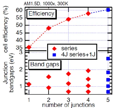
Theoretically, the more subcells with different bandgaps, the higher the efficiency. For infinite number of junctions, the theoretical efficiency of multi-junction solar cells reaches 86.8%8–10. Figure 1.4 shows the
theoretical efficiency as a function of the number of subcells, along with the bandgap combination to reach such efficiency (from an NREL lecture11). A 4-junction solar cell can theoretically reach an efficiency above 55 %, we must find the adequate 4 materials that have the right 4 bandgaps. But in real configuration, materials with different bandgaps do not necessarily have similar lattice parameters.
Figure 1.4 - Theoretical maximum efficiency of a multijunction as a function of the number of junctions, along with the corresponding bandgaps (NREL) 11
6
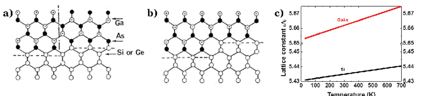
Figure 1.5 shows a list of available materials, with their lattice parameters and their bandgap, including the main III-V alloys, as well as Si and Ge. One can notice a wide disparity in bandgaps and lattice parameters. We see that Ge is almost lattice-matched with GaAs, hence the use of Ge as a substrate for most multi-junction solar cells based on GaAs family compounds. By following the vertical line between GaAs and AlAs, the AlxGa1-xAs family allows tuning the bandgap, while remaining almost lattice-matched with GaAs and Ge. However, most of the other materials have their own lattice parameter. Lattice-mismatch induces dislocations, grain boundaries or other types of impurities, that will highly reduce the efficiency 9.
Most of the research has been focused on the growth of lattice-matched materials, which are the easiest to manufacture. The very mature industry of high quality of III-V materials along with their strong absorption due to their direct bandgap gives to this type of materials the best properties for MJSC. It is also possible to use lattice mismatched materials by means of wafer bonding, or by using buffer layers. These technical paths are discussed in the following part.
I.1.2. Multi-junction solar cells: review
Multi-junction solar cells based on III-V materials hold the highest efficiency record. They correspond to the purple data plot in the NREL efficiency chart presented in Figure 1.2. It is the only technology that reached and overcame 30 % of efficiency. For example, 3-junction solar cells efficiency has increased by about 1% absolute per year since 2002. The graph also shows how using concentrating photovoltaics can boost the conversion efficiency of a III-V MJSC. The last 3-JSC record at one sun is reported to be 37.9 %12, while under concentration (302 sun) it reached 44.4%13.