HAL Id: tel-01996999
https://tel.archives-ouvertes.fr/tel-01996999
Submitted on 28 Jan 2019
HAL is a multi-disciplinary open access
archive for the deposit and dissemination of
sci-entific research documents, whether they are
pub-lished or not. The documents may come from
teaching and research institutions in France or
abroad, or from public or private research centers.
L’archive ouverte pluridisciplinaire HAL, est
destinée au dépôt et à la diffusion de documents
scientifiques de niveau recherche, publiés ou non,
émanant des établissements d’enseignement et de
recherche français ou étrangers, des laboratoires
publics ou privés.
pour la conception des filtres : Application aux filtres du
domaine automobile
Marine Stojanovic
To cite this version:
Marine Stojanovic. Etude et modélisation des couplages inter-composants pour la conception des
filtres : Application aux filtres du domaine automobile. Electronique. INSA de Rennes, 2018. Français.
�NNT : 2018ISAR0014�. �tel-01996999�
T
HESE DE DOCTORAT DE
L’INSA
RENNES
C
OMUEU
NIVERSITEB
RETAGNEL
OIREE
COLED
OCTORALE N°
601
Mathématiques et Sciences et Technologies
de l'Information et de la Communication
Spécialité : Electronique
Study and Modeling of Inter-Component Coupling for Filter Design
Application to Automotive EMI filters
Thèse présentée et soutenue à Angers, le 14 Septembre 2018
Unité de recherche : IETR
Thèse N° : 18ISAR 15 / D18 – 15
Par
Marine STOJANOVIC
Rapporteurs avant soutenance :
Geneviève DUCHAMP Professeur des Universités Université de Bordeaux Christian VOLLAIRE Professeur des Universités
Ecole Centrale de Lyon
Composition du Jury :
Président
Philippe BESNIER Directeur de Recherche CNRS IETR – INSA de Rennes Geneviève DUCHAMP Professeur des Universités
Université de Bordeaux Christian VOLLAIRE Professeur des Universités
Ecole Centrale de Lyon
Alain REINEIX Directeur de Recherche CNRS XLIM – Université de Limoges Olivier MAURICE Expert CEM (HDR) – Ariane Group
Directeur de thèse
Richard PERDRIAU Enseignant-Chercheur HDR IETR – ESEO
Co-directeur de thèse
Frédéric LAFON Master Expert CEM (HDR) – Valeo
Co-encadrant de thèse
Mohamed RAMDANI Enseignant-Chercheur HDR IETR – ESEO
Invités
Guillaume DEVAUCHELLE Vice-président Groupe Innovation et Développement Scientifique – Valeo Jean-Luc LEVANT Senior Expert CEM – Microchip François DE DARAN Senior Expert CEM
Intitulé de la thèse :
Study and Modeling of Inter-Component Coupling for Filter Design
Application to Automotive EMI filters
Marine STOJANOVIC
En partenariat avec :
Introduction
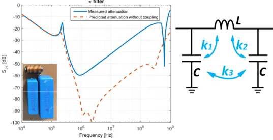
Les véhicules hybrides et électriques connaissent un essor considérable ces dernières années. De ce fait, de plus en plus d’électroniques et plus particulièrement des électroniques de puissance, sont utilisées dans nos véhicules. Face à cette densification de l’électronique dans un espace toujours aussi restreint, les problèmes de compatibilité électromagnétique (CEM) s’accentuent. En effet, les systèmes d’électronique de puissance sont des sources typiques d’interférences électromagnétiques. Ainsi, afin de réduire ces perturbations électromagnétiques, des filtres doivent être implémentés dans le but de les atténuer et, de ce fait, rendre conforme un équipement, selon les normes qui régissent la CEM. S2 1 [d B ]
C
C
L
k
1
k
2
k
3
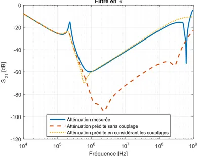
Figure 1 – Comparaison entre l’atténuation mesurée et l’atténuation prédite sans tenir compte des couplages
Les filtres pour la CEM, sont généralement constitués de composants passifs tels que les conden-sateurs, les inductances et les tores de mode commun (TMCs). Ces filtres doivent être dimensionnés au cas par cas, selon l’application et l’atténuation requise. Cependant, de nombreux paramètres peuvent avoir une influence non négligeable sur les performances d’un filtre. Parmi ces paramètres influents, le routage ou bien la mécanique peuvent fortement dégrader les performances du filtre. Afin de prendre en compte ces éléments, la simulation électromagnétique 3D est une bonne
solu-pour effectuer ce type de simulations.
Un paramètre qui influe également sur la performance d’un filtre, est la proximité des compo-sants les uns par rapport aux autres, ou autrement dit les couplages inter-compocompo-sants. En effet, la Fig. 1 présente la différence qu’il existe entre l’atténuation mesurée et l’atténuation prédite sans tenir compte des couplages inter-composants. L’écart est significatif (30dB à 10MHz) et une telle erreur de prédiction peut entrainer d’importants problèmes de design car le filtre sera sous-dimensionné pour l’application.
La plupart des travaux menés jusqu’ici sont basés sur des simulations électromagnétiques 3D et le désavantage de ces simulations est qu’elles prennent un temps considérable à la fois pour la construction des modèles mais également pour la résolution. De ce fait, à chaque modification de design, le calcul doit de nouveau être lancé, ceci jusqu’à trouver une solution satisfaisante, et donc cette méthode peut prendre plusieurs jours. De plus, un grand nombre d’informations sont nécessaires sur les composants, tels que la géométrie exacte ou bien les propriétés des matériaux. En règle générale, ces informations sont difficiles à obtenir et donc les modèles 3D sont compliqués à construire.
L’objectif qui émane de cette problématique est le besoin de développer une méthode sim-plifiée et rapide qui permettent de prédire les performances d’un filtre en tenant compte de son implémentation et quelle que soit sa structure.
Expression analytique simplifiée d’un couplage magnétique
Afin de déterminer une inductance mutuelle, ou bien de façon plus générale, un couplage magné-tique, le principe est le suivant (Fig. 2) : lorsqu’un courant i circule dans un composant, un champ magnétique B est généré et est couplé par le second composant à travers sa surface équivalente de couplage S. Le lien qu’il existe entre ces deux composants est appelé une mutuelle inductance M (Eq. 1). − → B ·−→S = M.i (1)i
B
S
M
Figure 2 – Principe pour déterminer une inductance mutuelle
De cette équation découlent donc les différentes thématiques de la thèse qui sont la détermina-tion d’une surface équivalente de couplage, le calcul du champ magnétique généré par un composant passif, dans le but de prédire une inductance mutuelle entre deux composants. Finalement, l’en-semble des inductances mutuelles entre les composants d’un même filtre devront être prises en compte pour prédire les performances du filtre.
Détermination de surface équivalente de couplage pour les
composants passifs
Une surface équivalente de couplage permet de représenter la sensibilité au champ magnétique d’un composant, autant en ce qui concerne le niveau de sensibilité que sa direction privilégiée. Pour déterminer cette surface équivalente, une méthode utilisant des mesures en cellule TEM a été développée. En effet, lorsque la cellule TEM (Fig. 3) est alimentée via une source RF (radio-fréquence) tel qu’un VNA (Analyseur de réseaux vectoriel), un champ électromagnétique uniforme est généré en cette cellule. De ce fait, il est possible de connaitre la valeur, le sens et la direction du champ magnétique dans la cellule.Ainsi, la sensibilité des composants passifs sous des conditions de champ magnétique maitrisées peut être étudiée. Finalement, une surface équivalente de couplage pour chaque composant pourra être extraite afin de réutiliser ce type de caractérisation.
Port 1 VNA Cellule TEM Septum Port 2 - VNA 50Ω ETEM HTEM 50Ω k
Figure 3 – Cellule TEM
Surface équivalente de couplage d’un condensateur
Pour déterminer la surface équivalente de couplage d’un condensateur, il est nécessaire de carac-tériser le composant pour ses deux orientations privilégiées : lorsque la surface de couplage et le champ magnétique sont colinéaires et dans le même sens, et la seconde lorsqu’ils sont dans des sens opposés. Ces deux mesures sont nécessaires afin de pouvoir supprimer la contribution du champ électrique. En effet, un fort champ électrique est présent en cellule TEM et son influence doit donc être supprimée, par calcul, pour se focaliser uniquement sur l’influence du champ magnétique.
Structure interne
Surface équivalente Surface équivalente
La direction privilégiée de couplage pour le condensateur est déterminée en effectuant des mesures tout autour du composant. Il s’est avéré que la surface de couplage d’un condensateur est localisée entre ses deux pins, le plan de masse et sa structure interne (Fig. 4).
De ce fait, à moins de connaitre la structure interne du condensateur, la meilleure façon pour déterminer sa surface équivalente de couplage est d’effectuer des mesures en cellule TEM.
Surface équivalente de couplage d’une inductance
Pour les inductances, le principe est le même que pour les condensateurs. Deux mesures sont nécessaires, pour les deux directions privilégiées du couplage au champ magnétique. Il a ainsi été déduit que la surface équivalente de couplage d’une inductance est orientée comme ses spires (Fig. 5).
S
ecFigure 5 – Direction de la surface équivalente de couplage d’une inductance
A partir des mesures en cellule TEM, sur de nombreuses inductances, les paramètres dimen-sionnant la surface équivalente de couplage d’une inductance ont été identifiés, à savoir : le nombre de spires N, la surface d’une spire Sspireet la perméabilité du matériau magnétique µr(Eq. 2).
Sec= N.Sspire.µr (2)
Pour une inductance verticale, le principe reste le même. Celle-ci doit être caractérisée de telle sorte à ce que sa surface équivalente de couplage et le champ magnétique soient colinéaires.
Finalement, à moins de connaitre ou de pouvoir estimer la perméabilité du matériau magné-tique, les mesures en cellule TEM restent la meilleure solution pour déterminer une surface de couplage.
Surfaces équivalentes de couplage d’un TMC
Quant aux TMCs, le principe est un peu plus complexe, du fait de sa géométrie et du fait qu’ils possèdent deux bobines distinctes. Une étude préliminaire a d’ailleurs été effectuée pour les deux modes de fonctionnement d’un TMC : le mode commun (MC) et le mode différentiel (MD). Pour ce faire, la caractérisation s’effectue tout autour du composant. La Fig. 6 présente les résultats des forces électromotrices générées au TMC en MC et en MD selon l’orientation du composant dans la cellule TEM. Il est alors clairement identifiable que le couplage lorsque le TMC est connecté en MC est bien plus faible et n’a pas de direction privilégiée comparée au MD. Il peut donc en être déduit, qu’un modèle représentant uniquement le MD, est suffisant pour modéliser un TMC.
10-4 10-3 10-2 m | [V ] fem extraites à 100kHz MC MD 0 50 100 150 200 250 300 Angle [°] 10-7 10-6 10-5 |f e m
Figure 6 – Forces électromotrices générées à un TMC à 100kHz pour le MC et le MD Afin de modéliser finement le TMC en MD, dix surfaces équivalentes de couplage (cinq par bobinage) vont être prises en compte (Fig. 7). Ces dix surfaces ont une position et direction fixes et ainsi, il ne reste qu’à déterminer l’amplitude des surfaces de couplage. De ce fait, douze mesures en cellule TEM sont nécessaires (à douze orientations différentes en cellule TEM), afin de déterminer les dix surfaces de couplages (deux mesures pour la suppression de l’influence du champ électrique et les dix autres pour la détermination des surfaces de couplage).
S1 S2 S3 S4 S5 S6 S7 S8 S9 S10
Figure 7 – Modèle de couplage équivalent d’un TMC en MD
Calcul analytique de champ magnétique généré par un
com-posant passif
Maintenant qu’une méthode a été définie pour déterminer une surface équivalente de couplage, la deuxième étape est de pouvoir estimer la valeur du champ magnétique généré par un composant passif. Pour ce faire, le modèle équivalent de couplage peut être réutilisé en tant que modèle d’émission, grâce au théorème de réciprocité.
n’importe quel type de contour (Eq. 3). Le calcul du champ magnétique avec la loi de Biot et Savart restera valide tant que le courant peut être considéré constant. Cette condition dépend de la valeur de la vitesse de propagation et ainsi que des matériaux (magnétiques, diélectriques).
−→ dB= µ 4π ˆr r2I −→ dS (3)
De plus, afin de correctement prédire le champ magnétique généré par un composant, il est indispensable de prendre en compte l’influence du plan de masse (si tel est le cas). De ce fait, la théorie des images doit être appliquée afin de pouvoir prendre en compte l’influence d’un plan de masse.
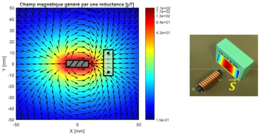
Pour chaque type de composant passif (condensateurs, inductances horizontales et verticales, tores de mode commun horizontaux et verticaux), les surfaces équivalentes de couplages sont alors réutilisées pour déterminer la valeur du champ magnétique qu’il génère. La Fig. 8 présente diffé-rents exemples de champs magnétiques générés par un condensateur, une inductance et un TMC. L’ensemble de ces calculs ont été validées par des mesures à l’aide d’un scanner champ proche.
Y [ m m ] Y [ m m ] Y [ m m ]
Figure 8 – Champs magnétiques générés par un condensateur, une inductance et un TMC en MD Il est important de remarquer que le champ magnétique d’un TMC n’est calculé que pour le MD. En effet, comme le TMC en MC ne permet que peu de couplage magnétique comparé au MD, le TMC en MC génèrera donc peu de champ magnétique (théorème de réciprocité).
Calcul d’une mutuelle inductance entre deux composants
pas-sifs
Avec les deux thématiques précédentes (surface équivalente de couplage et champ magnétique généré par un composant passif), il est désormais possible de calculer une inductance mutuelle entre deux composants, quelle que soit leur position et leur orientation. En effet, l’Eq. 1 peut être appliquée directement.
Prenons l’exemple d’un cas très simple de calcul d’une mutuelle inductance entre une inductance et un condensateur, espacés de 25mm l’un de l’autre (Fig. 9).
25mm
Figure 9 – Exemple d’une inductance et d’un condensateur espacés de 25mm
Chacun des composants est caractérisé au préalable, en termes d’impédance et en cellule TEM. Ainsi, le champ magnétique généré par l’inductance est calculé au niveau de la surface de couplage du condensateur (Fig. 10). Le cheminement inverse donnera le même résultat, en accord avec le théorème de réciprocité. Y [ m m ] Y
Figure 10 – Champ magnétique de l’inductance sur la surface de couplage du condensateur De cette manière, une valeur constante de la mutuelle qui existe entre ces deux composants peut être extraite. Cette valeur sera alors valable tant que les conditions de la magnéto-statique sont respectés. La Fig. 11 présente la comparaison entre cette valeur d’inductance mutuelle extraite par le calcul et celle extraite par la mesure. Ce type de comparaison a été effectuée pour de nombreux composants passifs, et ainsi la méthode de calcul de mutuelles est validée.
10-8 10-7 e m u tu e lle [ H ]
Inductance mutuelle entre L et C
Extraite par la mesure Extraite par le calcul
105 106 107 108 Frequence [Hz] 10-9 10 In d u c ta n c e Domaine d’extraction
Figure 11 – Comparaison entre l’inductance mutuelle extraite par la mesure et par le calcul
Prédiction de l’atténuation d’un filtre quelle que soit sa
struc-ture et sa topologie
Désormais, quelle que soit la position des composants les uns par rapport aux autres, il est possible de calculer les mutuelles inductances entre eux, deux par deux. Le grand avantage de cette méthode est que, une fois les composants caractérisés, le calcul de couplage entre les composants est direct et très rapide.
La méthode qui a été choisie pour le calcul d’atténuation d’un filtre, est la MKME (Méthode de Kron Modifiée pour la Compatibilité Électromagnétique). Cette méthode, basée sur l’analyse tensorielle des réseaux est très puissante et permet de décrire n’importe quel système quelle que soit sa complexité. L’avantage majeur de la méthode de Kron est que la filtre peut être décrit en distinguant bien les paramètres intrinsèques au filtre (les composants et leurs éléments parasites) et les paramètres modifiables (les couplages entre les composants). De plus, il existe une infinité de structures et de topologies possibles pour les filtres. De ce fait, un algorithme générique de création de graphe pour le calcul d’atténuation. De cette manière, il est possible de calculer l’atténuation d’un filtre, en MC et MD, quelle que soit sa structure, quelle que soit sa topologie. L’intérêt d’avoir développer une méthode générique est que l’ensemble de cette méthode est capitalisée en un seul outil permettant la prédiction de performance d’un filtre. Cet outil est opérationnel et actuellement utilisé par les ingénieurs design pour l’intégration des filtres.
Afin d’illustrer cette méthode, reprenons l’exemple de l’introduction (Fig. 1) d’un filtre en Pi, composé d’un condensateur, suivi d’une inductance puis d’un second condensateur. L’analyse ayant été effectuée, il est alors possible de prédire les performances de façon très précise (Fig. 12).
Ce simple exemple illustre bien les possibilités de calcul de cette méthode. Des cas bien plus complexes ont été traités et validés, tels que des filtres composés de plusieurs centaines d’induc-tances mutuelles.
-60 -40 -20 0 1 [d B ] Filtre en 104 105 106 107 108 109 Fréquence [Hz] -120 -100 -80 S 2 1 Atténuation mesurée
Atténuation prédite sans couplage
Atténuation prédite en considérant les couplages
Figure 12 – Prédiction des performances du filtre en Pi
Conclusion
L’objectif principal de cette thèse était de développer une méthode analytique afin de prédire les performances d’un filtre en tenant compte de sa topologie. Pour ce faire, le travail a été divisé en quatre grandes étapes : la détermination de surfaces équivalentes de couplage des composants pas-sifs constituant le filtre, le champ magnétique qu’ils génèrent pour finalement prédire un couplage magnétique entre deux composants. La dernière étape a été de développer un algorithme générique permettant le calcul d’atténuation d’un filtre, en considérant les couplages entre les composants, quelle que soit sa structure. Finalement, cette méthode a été appliquée et validée sur de nombreux cas d’applications.
L’ensemble de la méthode a été capitalisée via un outil nommé GFD (Global Filter Design), présenté en Fig. 13. Cet outil permet le calcul d’une simple mutuelle inductance entre deux com-posants, ou bien la prédiction d’atténuation d’un filtre.
Résumé en Français 1
Introduction 19
1 Main concept of EMI filter design 27
1.1 Introduction to the main concept of EMI filter design . . . 28
1.2 EMI noise sources . . . 28
1.3 EMI filters . . . 30
1.3.1 Filter attenuation signification . . . 30
1.3.1.1 Analytical calculation . . . 31
1.3.1.2 Attenuation measurement . . . 33
1.3.2 Filter structures . . . 34
1.3.2.1 Filter structures dedicated to low input and output impedances of the system regarding the filter position . . . 34
1.3.2.2 Filter structures dedicated to low input and high output impedances of the system regarding the filter position . . . 35
1.3.2.3 Filter structures dedicated to high input and low output impedances of the system regarding the filter position . . . 35
1.3.2.4 Filter structures dedicated to high input and output impedances of the system regarding the filter position . . . 36
1.3.3 Influence of input and output impedances on filter attenuation . . . 36
1.4 Modeling of passive components . . . 39
1.4.1 Impedance measurement . . . 39
1.4.2 Capacitor . . . 41
1.4.3 Inductor . . . 43
1.4.4 Common mode choke . . . 47
1.4.4.1 Classic model . . . 48
1.4.4.2 Multi-resonance model . . . 50
1.4.4.3 Dispersion model . . . 51
1.5 Conclusion . . . 54
2 Equivalent coupling models of passive components 55 2.1 Introduction to the equivalent coupling model principle . . . 56
2.2 The TEM cell . . . 56
2.2.2 Magnetic field measurement in the TEM cell . . . 58
2.3 DUT measurements in the TEM cell . . . 61
2.3.1 Definition of the normal to the coupling surface . . . 61
2.3.2 Measurements to be carried out on the DUT . . . 63
2.4 Extraction of the equivalent coupling surface . . . 64
2.4.1 Subtraction of the electric field contribution . . . 64
2.4.2 Integration of the impedance of the DUT . . . 65
2.4.3 Extraction of the equivalent coupling surface . . . 66
2.5 Application case: the capacitor . . . 68
2.5.1 Measurements performed on the DUT . . . 68
2.5.2 Measurement post-processing . . . 68
2.5.3 Geometrical approximation . . . 69
2.5.4 Validation of the coupling model with a uniform magnetic field . . . 70
2.5.5 Particular case of MLCC capacitors . . . 71
2.6 Application case: the inductor . . . 72
2.6.1 Measurements performed on the DUT . . . 73
2.6.2 Measurements post-processing . . . 73
2.6.3 Geometrical approximation . . . 74
2.6.4 Extraction of the magnetic permeability . . . 75
2.6.5 Validation of the coupling model with a uniform magnetic field . . . 76
2.6.6 Vertical inductor . . . 77
2.7 Application case: the common mode choke . . . 77
2.7.1 Differential mode analysis . . . 78
2.7.2 Common mode analysis . . . 80
2.7.3 Comparison between DM and CM analyze . . . 81
2.7.4 DM coupling model of a CMC . . . 82
2.7.4.1 Coupling model definition . . . 82
2.7.4.2 Extraction of the DM permeability of a toroidal core . . . 84
2.7.4.3 Extraction of the coupling model at a fixed frequency . . . 84
2.7.4.4 Extraction of the coupling model over frequency . . . 84
2.7.5 Validation of the coupling model with a uniform magnetic field . . . 85
2.7.6 Vertical common mode choke . . . 86
2.8 Conclusion . . . 87
3 Estimation of the mutual inductance between two passive components 89 3.1 Introduction to the mutual inductance estimation . . . 90
3.2 Magnetic field calculation principle . . . 90
3.2.1 Biot & Savart Law . . . 90
3.2.2 Reciprocity principle . . . 91
3.2.3 Image theory . . . 92
3.2.4 Scope of application . . . 93
3.2.5 Application case : the capacitor . . . 94
3.2.6 Application case : the inductor . . . 96
3.2.6.1 Horizontal inductor . . . 96
3.2.7 Application case : the common mode choke . . . 99
3.2.7.1 Horizontal common mode choke . . . 100
3.2.7.2 Vertical common mode choke . . . 100
3.3 Prediction of mutual inductance . . . 101
3.3.1 Between two capacitors . . . 101
3.3.2 Between two inductors . . . 104
3.3.3 Between two CMCs in DM . . . 105
3.3.4 Conclusion . . . 107
3.4 Extension of the method to self-inductance prediction . . . 108
3.4.1 Introduction to the self-inductance prediction . . . 108
3.4.2 Straight coil . . . 108 3.4.2.1 Analytical formulation . . . 110 3.4.2.2 Validation by measurements . . . 111 3.4.3 Toroidal coil . . . 112 3.4.3.1 Analytical formulation . . . 113 3.4.3.2 Validation by measurements . . . 113 3.5 Conclusion . . . 114
4 Prediction of the filter attenuation considering inter-component coupling 117 4.1 Introduction to the prediction of the filter attenuation considering inter-components coupling . . . 118
4.2 Modified Kron’s Method applied to EMC (MKME) . . . 118
4.2.1 Graph construction . . . 118
4.2.2 Calculation of tensors and matrices . . . 121
4.2.3 Resolution . . . 122
4.3 Generic Kron’s graph development . . . 123
4.3.1 Global parameters . . . 124
4.3.2 Determination of the number of nodes . . . 124
4.3.2.1 Number of nodes in DM . . . 125
4.3.2.2 Number of nodes in CM . . . 126
4.3.3 Determination of the number of edges . . . 127
4.3.4 Definition of the impedance tensor . . . 128
4.3.4.1 Intrinsic impedance tensor . . . 128
4.3.4.2 Coupling tensor . . . 129
4.3.5 Definition of the source tensor . . . 130
4.3.6 Definition of the connectivity matrix : the transfer matrix between the edge and the mesh space . . . 130
4.3.6.1 Determination of meshes and connectivity matrix in DM . . . 131
4.3.6.2 Determination of meshes and connectivity matrix in CM . . . 132
4.3.7 Transformation and attenuation calculation . . . 134
4.4 Application case : attenuation of a LC filter and its optimization . . . 135
4.5 Application case : Pi filter on a LED driver for a DC/DC converter . . . 140
4.6 Application case : OBC (On Board Charger) H filter . . . 141
4.7 Application case : Power filter application . . . 145
Synthesis and conclusions 149
Bibliography 151
A Tools development 157
A.1 Equivalent Surface Extractor - Measurement bench . . . 157
A.2 Global Filter Design . . . 161
A.2.1 Component menus . . . 162
A.2.2 Component connections . . . 165
A.2.3 Calculation of filter performance . . . 165
B Magnetostatic field calculation 167 B.1 Application case: Capacitor . . . 167
B.2 Application case: horizontal inductor . . . 169
B.3 Application case: vertical inductor . . . 170
B.4 Application case: horizontal common mode choke . . . 171
B.5 Application case: vertical common mode choke . . . 172
Je tiens à remercier tous les membres du jury, Geneviève Duchamp, Christian Vollaire, Alain Reineix, Olivier Maurice, Philippe Besnier, Guillaume Devauchelle, Jean-Luc Levant, François De Daran et Xavier Bunlon pour tout l’intérêt que vous avez porté à mon travail. Merci partic-ulièrement à Geneviève Duchamp et Christian Vollaire d’avoir accepté d’en être rapporteur ainsi que de m’avoir permis de soutenir ma thèse.
Ces trois années ont été très riches. J’ai beaucoup appris, en CEM bien évidemment, mais également et surtout sur moi-même. Je suis profondément convaincue que ce qui nous caractérise en tant que personne, autant profesionnellement que personnellement, ne vient pas que de nos aptitudes ou de notre caractère. Les personnes que nous rencontrons et qui nous accompagnent au quotidien dimensionnent cette image que nous renvoie le miroir. Et dans cette aventure, je pense avoir eu beaucoup de chance. Beaucoup de chance de rencontrer, d’être accompagnée et entourée par les bonnes personnes.
Frédéric, tu es sans aucun doute celui à qui je pense en premier. Tu m’as fait confiance, m’as donnée ma chance, m’as guidée et accompagnée durant ces trois ans. Tu m’as également poussée dans mes retranchements pour que je donne le meilleur de moi-même, et je t’en suis profondément reconnaissante. Je suis certaine que ces trois années ne sont qu’une préface.
Mohamed et Richard, merci à vous deux de m’avoir si bien guidée, pour votre disponibilité et votre rigueur. Vous aurez été tous les deux, de très bons guides. J’espère que nous continuerons à travailler ensemble.
Merci à mes chers collègues Candice, Priscila, David et Van pour tous ces moments de partage, de complicité et de franche rigolade. Merci à tous mes collègues du laboratoire CEM, qui rendent le quotidien agréable, par leur bonne humeur et leur envie d’avancer ensemble.
Je pense également aux belles rencontres que j’ai pu faire pendant les conférences. Merci à ceux en qui on se retrouve et avec qui on partage la même passion de la recherche.
Enfin, je ne saurais concevoir ces remerciements sans y inclure ceux qui sont si chers à mes yeux.
Merci à mes chers amis, avec qui je partage toujours des moments inoubliables. Merci à ma Luna, mon réconfort. Merci à ma famille, mon indéniable soutien. Merci à mes beaux-parents, Catherine et Jean-Louis, ma belle-soeur, Mélissa, mon beau-frère, Gauthier. Un grand merci à ma grande-tante, Françoise, pour tous ces moments partagés, telle une grand-mère et sa petite fille. Merci à Isa, à mes grands-parents, Negosava et Dusan, mes chers cousins, Johanna et Guillaume, Rémy et Silvia, Alexandre et Célia, mes oncles et tantes, Slavica, William, Goran.
Et pour finir... Les derniers cités mais sans aucun doute les plus chers à mon coeur. Merci ma Soeur, mon soleil. Toi qui m’as fait tant rire en pensant que je pourrais te faire des ordonnances
Merci Papa, mon sourire. Toujours le mot pour rire. Il aura fallu quelques temps avant que la CEM ne soit plus un acronyme inconnu pour toi! Merci Maman, mon modèle. Toi qui m’accompagne. La femme à qui j’aimerais ressembler un jour. Et pour finir, mon Guillaume, mon pilier. Merci... Merci pour tout, pour ton soutien, ta force, ta patience et pour tout le bonheur que tu me donnes en partageant ma vie.
Context of the study
With the continuous progress of hybrid and electrical vehicles, power electronics are becoming widely used in the automotive domain. Power electronics are typical sources of electromagnetic interferences (EMI) and, therefore, well designed filters are required to reduce all those emissions. The main role of a filter is to attenuate disturbances in order to comply with international standards and, therefore, to obtain an EMC-compliant equipment, and particularly a CISPR25-compliant system for automotive domain [1].
Figure 14: EMI filter examples in power electronics
All filters are different and are designed case per case according to the specific needs. However, there are several parameters that can influence the filter performance.
One of those parameters is the coupling between the traces. Actually, that parameter has an influence on the final filter performance as described in [2]. It can be dealt with 3D electromagnetic simulation as presented in Fig. 15.
Figure 15: Different filter topologies for a structure, considering PCB traces [2]
Another parameter that have an influence on filter performance is the mechanical structure that can enclose the filter. This part can also be studied with 3D simulation. Actually, it does not require a lot of information on the component or on the material properties. It just requires the 3D geometry coming from other study, like CAD (Computed-Aided Design) design. Fig. 16 presents an example of the 3D model considering the PCB traces and also the housing.
Figure 16: Example of 3D modeling including PCB traces and housing for an AC filter Then, one of the most destructive parameter, in terms of filter performance, is the inter-component coupling as presented in [3, 4, 5, 6, 7]. Actually, it is presented in Fig. 14 different filter examples where it is clearly identifiable that the components are very close from each other. This proximity induces magnetic coupling between components and has a big influence on the final filter performance. Let’s take the example from Fig. 17 which presents the difference between the predicted attenuation without considering those inter-components coupling and the measurement.
S2 1 [d B ]
C
C
L
k1
k2
k3
Figure 17: Comparison between the predicted attenuation without considering inter-component coupling and the measured attenuation of a Pi filter
The difference between the predicted attenuation without coupling and the measured attenua-tion is significant. Thus, a filter which is designed without considering the components proximity, can be finally insufficient to reduce the EMI noises. In such case, additional work must be per-formed like layout modification or mechanical enclosure. Therefore, in order to avoid those kind of additional works, the integration and the components placement must be considered to have a
The majority of studies done on inter-component coupling is based on 3D electromagnetic simulation like in [4, 8, 9, 10, 11, 12, 13, 14, 15, 16, 17, 18]. This methodology can be very accurate, but is time consuming for model construction and solving. Furthermore, this kind of simulation requires too much information on the components to build a 3D model.
(a) (b)
Figure 18: 3D model of a- inductor b- capacitor [4]
A lot of information on components is required and the model must be very accurate regarding actual components (Fig. 18). All the components must be modeled in detail, going through geometry but also the properties, internal structure etc.
Current concentration
Figure 19: Multilayer capacitor model for 3D electromagnetic simulation [4]
Fig. 19 presents an example that shows the high level of accuracy which is required in terms of modeling in order to obtain good results. All this kind of work is difficult to establish and time consuming. Furthermore, all the filters must be studied case per case and there is no generic methodology for filter design.
simplified method for filter design, not based on 3D modeling and generic enough to deal with any kind of structures and topologies.
Inter-component coupling in filter design
Inter-component coupling in a filter design plays a major role on filter performance. Then, in order to model a complete filter, the equivalent electrical models of passive components must be considered, but it is not sufficient. The magnetic couplings between the components are mandatory in order to have a good prediction of filter performance.
Actually, the mutual inductance M (Eq. 4), or more generally a coupling coefficient k, is a link between two inductances L1 and L2, which represents a magnetic coupling.
M = kpL1.L2 (4)
A mutual inductance between two inductances can be represented as in Fig. 20-a. Actually, a magnetic coupling can also be represented as an electromotive force generated to the components (Fig. 20-b).
L
1L
2M
-jω
M
i
2-jω
M
i
1+
-+
-i
1i
2i
1i
2L
1L
2-jω
M
i
-jω
M
i
(a) (b)Figure 20: Two different ways to represent a mutual inductance
Those mutual inductances have a high influence on the filter attenuation as highlighted in Fig. 17 and, therefore, they must be considered.
Coupling minimization
The first idea, in order to avoid the degradation coming from the magnetic coupling between components, is to reduce couplings. To minimize those couplings, the first step is to understand how the components radiate and how the components couple the magnetic field. Each type of component has a preferred orientation (or several) in emission and by reciprocity in coupling [19]. A first example for two capacitors in Fig. 21 is presented.
B
S
B
S
B
B
(a) (b)Figure 21: a- High b- Low coupling between two capacitors
When two capacitors are face to face as in Fig. 21-a, the magnetic field generated by the first component is coupled to the second one, through its equivalent coupling surface. Thus, the magnetic coupling between both components is high. However, when both components are perpendicular like in Fig. 21-b, the majority of the magnetic field generated by the first component does not pass through the coupling surface and, therefore, the magnetic coupling is significantly reduced.
For an inductor and a CMC in DM, the principle is the same as for capacitors. The preferred orientation of the magnetic field generated by the first component and the preferred orientation of the coupling to the second component are determined, as presented in Fig. 22 and Fig. 23. The coupling for CMC is only considered in DM because CM does not allow a high coupling compared to DM. This point will be detailed in Sect. 2.7 dedicated to the determination of the equivalent coupling model of a CMC.
B
S
B
S
B
S
(a) (b)B
S
S
S
B
S
(a)
B
(b)
Figure 23: a- High b- Low coupling between two CMCs in DM
As for capacitors, in order to minimize the coupling between two inductors or two CMCs, the component can be turned by 90° as presented in the two previous figures. This reasoning can also be applied for coupling minimization between a capacitor and an inductor, a capacitor and a CMC, etc. This comes from the knowledge of emission direction and coupling direction as presented in [19].
In filter design, to avoid the degradation coming from inter-component coupling, a first step can be the minimization of coupling. This methodology can be applied when there are only two or three components. However, in a real world application, with significant room constraints, this minimization cannot be applied systematically. Indeed, the filter must be designed by considering inter-component coupling and by understanding and knowing which couplings are destructive or not.
Objectives of research studies
The objective of this thesis is to simplify coupling phenomena and to base reasoning only on analytical calculations and exploitation of measurements.
i
B
S
M
The principle which is going to be used is based on Eq. 5 and 6, where the mutual inductance
M can be expressed in Eq. 7, considering that p is the complex variable coming from the Laplace
transform. Actually, the mutual inductance can be estimated from the magnetic field created by the first component and the equivalent coupling surface of the second component. The flux φ created by the magnetic field B on the equivalent surface S are linked to the current by the mutual inductance M (Fig. 24). Eq. 7 clearly describes the different topics (Fig. 25).
dφ=−→B · d−→S =⇒ φ =−→B ·−→S (5) dφ dt = M di dt =⇒ L φ.p= M.i.p (6) − → B ·−→S = M.i (7)
Coming from Eq. 7, the main steps of the thesis work can be described.
The first chapter deals with the determination of an equivalent coupling surface or, more gener-ally, an equivalent coupling model. Actugener-ally, all types of components can have one, several or even no preferred orientation regarding magnetic field coupling. The second chapter is then dedicated to the magnetic field generated by passive components. A mutual inductance can be estimated using both previous topics and will be presented in Chapter 3. Finally, filter performance prediction considering magnetic coupling, with MKME (Modified Kron’s Method applied to Electromagnetic compatibility), will be presented in the last chapter. The methodology will be validated under different examples, through real world applications.
Coupling coefficient
extraction
Between Capacitors,Equivalent Coupling
Model
Capacitor, Inductor, CMCMagnetic field
calculation
Capacitor, Inductor, CMCImpedance
model
Capacitor, Inductor, Chapter n°2 Chapter n°3 Chapter n°3 Chapter n°1 Between Capacitors, Inductors, CMCs Capacitor, Inductor, CMCFilter attenuation
prediction
Whatever the structure Whatever the topology
Chapter n°4
Main concept of EMI filter design
Coupling coefficient extraction Equivalent Coupling Model Magnetic field calculation Chapter n°2 Chapter n°3 Chapter n°3 Chapter n°1Impedance model
Capacitor, Inductor, CMC Filter attenuation prediction Chapter n°4 CMC1.1
Introduction to the main concept of EMI filter design
The design of EMI filters is a key point for EMC (electromagnetic compatibility). Actually, those filters are needed in order to reduce the EMI (electromagnetic interferences) that come from EMI sources. Different structures of filter exist and, therefore, it must be designed case per case con-sidering the required noise attenuation. Finally, in order to build up filters, a good knowledge of passive components in terms of impedance is mandatory.Therefore, in this first chapter, some general and well-known basics of EMC are presented, such as EMI sources, EMI filters and passive components modeling.
1.2
EMI noise sources
There are two main types of noise sources: natural and artificial sources, as described in [20]. Natural sources gather the earth’s magnetic field, lightning or electrostatic discharge for example. Artificial sources can be intentional, such as radar, radio communication, television or medical equipment. There are also unintended sources coming from electronic devices that generate para-sitic emissions or from power electronics, with motor control for example. Here, only the unintended artificial noise sources are considered and, more particularly, noise sources coming from electronic and electric equipments.
There are two types of noise propagation that must be distinguished, differential mode (DM) and common mode (CM).
DM noise generally comes from power supply or switching cells. This mode is called the “normal” mode because functional signals are mostly defined in that mode. DM is characterized by currents flowing in the opposite direction for a pair (Fig. 1.1).
Source
N
Noise
L
o
a
d
N
Noise
source
Figure 1.1: DM propagation noise
As far as CM noise is concerned, it appears generally in high frequencies (beyond MHz). CM noise comes from parasitic capacitances between the equipment and its ground reference, as pre-sented in Fig. 1.2. CM noise is commonly named parallel mode because currents are in the same direction for a pair and flow back through the reference.
Source
N
Noise
source
Lo
a
d
source
Ground plane – Reference
Parasitic
capacitance
Parasitic
capacitance
Figure 1.2: CM propagation noise
Therefore, the filter structure must be chosen depending on the mode that requires to be filtered.
Actually, in order to identify the different noise sources and their level, SPICE (Simulation Program with Integrated Circuit Emphasis) simulation is a good solution. By considering parasitic elements, switching cells etc. it is possible to determine which noise is dominant and, therefore, identify the required filtering.
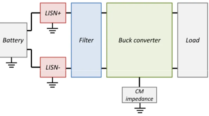
Let us take the example of the noise prediction of a buck converter. In order to perform that, Fig. 1.3 presents the block diagram of the simulation. It includes the different elements for conducted emission simulations which are widely developed in [21, 22, 23, 24, 25]. This block diagram is composed of a battery, two LISNs (for conducted emissions measurements), a filter, a buck converter, a load (which is in this case a resistor) and finally a CM impedance.
Filter Buck converter
LISN+ LISN-Battery Load LISN-CM impedance
Figure 1.3: Block diagram of noise perturbation estimation for a buck converter
A first step can be to estimate the conducted emissions coming from the buck converter without filtering. Thus, the voltages measured at LISNs level are directly the noise coming from the
Therefore, those voltages are used to extract the related DM and CM noises as presented in Fig. 1.4. Limit DM Noise Limit CM Noise
Figure 1.4: DM and CM noise coming from a Buck converter
It clearly appears that, for this particular example, the DM noise is dominant compared to the CM one. Actually, it comes from the switching cell of the converter. Nevertheless, the CM noise is not negligible and it mainly comes from the CM impedance. The limits that are presented in Fig. 1.4 are totally arbitrary and just allow to illustrate the filter design principle.
Actually, it appears that the DM noise overtakes the limit in the frequency band coming from 100kHz to 30MHz and must be reduced by at least 30dB at 200kHz. For the CM noise, it does not overtake the limit and, therefore, a filter more dedicated to DM attenuation must be integrated to the system. This filter must have an operational frequency band coming from 100kHz to 30MHz, and a minimum of 30dB attenuation at 200kHz.
Through this example, it was presented a methodology for CM and DM noises estimation. Considering the limits, the required filter performance is defined and, so, the filter will be de-signed in consequence. Therefore, the inter-components coupling, that have an influence on filter attenuation, must be considered in order to finally predict the real performances.
The main objective of the thesis work is to ensure that the implemented filter will provide the required attenuation on the correct frequency band.
1.3
EMI filters
1.3.1
Filter attenuation signification
The parameter that characterizes a filter is its attenuation in decibels (dB) and is measurable through its S21 parameter. This parameter corresponds to the transmission coefficient between the input and the output of the filter. The S parameters matrix can be defined as the ratio between the incident wave ai (Eq. 1.1), and reflected wave (Eq. 1.2), as it is described in Eq. 1.3 with
k 6= j.
ai=
Vi+ Z0Ii
bi= Vi− Z0Ii 2√Z0 (1.2) Sij = bi aj |ak=0 (1.3)
These S parameters for a two-port network can be presented as in Fig. 1.5 by considering E as an AC voltage and Z0 the characteristic impedance with Z0= Z1 = Z2 = 50Ω. Sii parameter
is the reflection coefficient of port i when all the other ports are terminated by characteristic impedances. The Sij parameter is the transmission coefficient from port j to port i considering
that all the other ports are terminated by characteristic impedances.
Z
2Z
1I
1I
2V
1V
2S
11S
22S
212 ports
Network
E
V
1V
2S
12Figure 1.5: S parameters of a two-port network
It must be noticed that it is mandatory to know input and output impedances in order to correctly build the filter. Those impedances have a major influence on filter attenuation as pre-sented in Sect. 1.3.3. It is necessary to characterize the filter under characteristic impedances, so
Z0= Z1= Z2= 50Ω, but it is also necessary to predict the filter attenuation considering the real
impedances, by simulation or calculation.
1.3.1.1 Analytical calculation
S parameters can be expressed as a function of currents and voltages presented in Fig. 1.5. Eq. 1.1, 1.2 and 1.3 can be summarized and applied to the two ports network.
• S11= ab11|a2=0, it can be considered that a2= 0 ⇔ V2+ Z0I2 = 0 and considering Kirchhoff
law, E = V1+ Z0I1 ⇒ S11=2VE1 −1
• S12= ab12|a1=0, it can be considered that a1= 0 ⇔ V1+ Z0I1 = 0 and considering Kirchhoff
law, E = V2+ Z0I2 ⇒ S12=2V1 E
• S21= ab21|a2=0, it can be considered that a2= 0 ⇔ V2+ Z0I2 = 0 and considering Kirchhoff
law, E = V1+ Z0I1 ⇒ S21=2VE2
• S22= ab22|a1=0, it can be considered that a1= 0 ⇔ V1+ Z0I1 = 0 and considering Kirchhoff
law, E = V2+ Z0I2 ⇒ S22=2VE2 −1
In order to simplify all these equations, the AC voltage E can be fixed at E = 2V . Indeed, the S parameters matrix can be presented as in Eq. 1.4.
[S] = S11 S12 !
= V1−1 V1 !
The output voltage of the two-port network is then the image of filter attenuation . It must be noticed that the result is a voltage ratio and is dimensionless.
There are two types of noise and so two types of filter. Indeed, the filter must connected in order to induce a DM or CM current, to extract its performance.
For the first case dedicated to DM noise, the filter must be connected in DM in order to extract its performance in the presence of a DM current. Fig. 1.6 shows how it can be done by using Fig. 1.5 and considering the two-port network as the filter.
Filter
E
Z
1i
1i
1Z
2i
2i
2V
2Figure 1.6: DM attenuation calculation
The AC source voltage E = 2V and the characteristic impedance Z1= 50Ω are located between both inputs and a characteristic impedance Z2= 50Ω is located between both outputs, in order to extract V2, the image of the DM attenuation.
Z
1Filter
i
1i
2i
1.αi
1.(1-α)i
2.αi
2.(1-α)Z
2E
V
2Figure 1.7: CM attenuation calculation
For the second case, the filter must be connected in CM in order to extract its performance in the presence of CM current. Indeed, both inputs are shorted and connected to a characteristic impedance Z1= 50Ω and the AC source voltage E = 2V . Outputs are also shorted and connected to a characteristic impedance Z2= 50Ω, as presented in Fig. 1.7. A CM current flows through the filter and, therefore, the voltage V2is the image of the CM attenuation considering that 0 < α < 1 the proportion of the current going on each edge (depending on impedances).
This kind of calculation can be performed with nodal analysis such as in a SPICE simulator, or using a modal analysis such as MKME. The choice here is to use a modal analysis as in [26, 27, 28], which is very practical in terms of speed of calculation and genericity [29].
Another advantage of MKME is that everything is configurable and all parameters are grouped and classified into two different categories: the intrinsic parameters and the modifiable ones. This point is very important because the difference is clearly made between all the fixed parameters (filter components and their parasitic elements) and all the modifiable ones (the coupling between the components).
Finally, it must be noticed that all the reasoning that will be presented is capitalized in a unique generic tool and, therefore, speed of calculation and genericity are mandatory.
Indeed, MKME appears as a good choice to study filter attenuation considering inter-component coupling. Consequently, it will be presented in detail in Chapter 4.
1.3.1.2 Attenuation measurement
The attenuation of a filter is measurable through its S21 parameter. The dedicated device is the VNA (Vector Network Analyzer) that can measure S parameters in magnitude and phase. The principle is to connect the filter input to the first port and the filter output to the second port and, thus, measure the corresponding S parameters (Fig. 1.8).
Port 1 Port 2
VNA
Filter
Figure 1.8: Filter attenuation measurement with a VNA
S11parameter is thus the reflection coefficient of the first port, S21the transmission coefficient
from the first port to the second one, S12the transmission coefficient from the second port to the first one and finally, S22 is the reflection coefficient of the second port.
Before performing any measurement, a VNA calibration must be done in order to compensate wire and connector effects. Indeed, the reference plane is located at the input and output of the filter in order to only measure the S parameters of the filter and not the filter including connections.
i
2 VNA Port 2i
2i
1 VNA Port 1i
1Filter
Figure 1.9: DM filter attenuation measurement
Both modes must be measured separately and Fig. 1.9 can be considered as a filter attenuation measurement in DM. Actually, this configuration induces a DM current to the filter and, therefore, its performance for a DM noise can be extracted. It must be noticed that a transformer is necessary
a part of the filter. Actually, the grounds of the two ports of the VNA are connected together and, thus, the transformer is mandatory to extract the real DM filter attenuation with the S21 parameter and not only a part of the filter.
i
1i
1.αi
1.(1-α) VNA Port 1i
2.(1-α)i
2i
2.α VNA Port 2Filter
Figure 1.10: CM filter attenuation measurement
The CM filter attenuation measurement is based on the same principle as in the previous subsection, the filter must be connected in order to induce a CM current. Fig. 1.10 presents this kind of measurement, both inputs are shorted and connected to the first port of the VNA, and both outputs are shorted and connected to the second port. Finally the S21 parameter represents the CM filter attenuation considering that 0 < α < 1 the proportion of the current going on each edge (depending on impedances).
Examples here are for SMA connectors making the link between the filter and the VNA.
1.3.2
Filter structures
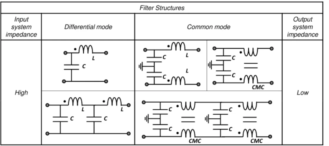
The main objective of a filter is to attenuate the disturbances generated by electronic equipment. To do so, the idea is to introduce an impedance discontinuity. For example, if the input and output impedances of the system, regarding the filter position, are low (regarding 50Ω), the goal is to integrate a filter with a high impedance. Typically, inductances and common mode chokes (CMCs) present high impedances whereas capacitors present low impedances.
Regarding the mode of the perturbation, the filter must be adapted for DM or CM or both. All the structures that are presented in the following subsections can be used on their own or by mixing them together. The structure has to be chosen according to the required attenuation. The higher the number of filter cells in cascade, the higher the filter order and, therefore, the better the filter performance. For instance, a single LC filter presents an ideal behavior of −40dB/decade whereas a double LC filter in cascade presents an ideal behavior of −80dB/decade.
In the following subsections, different filter structures are presented but are not exhaustive.
1.3.2.1 Filter structures dedicated to low input and output impedances of the system
regarding the filter position
The objective of a filter is to introduce an impedance discontinuity. The system presents low input and output impedances, regarding the filter position. Indeed, the filter should present high input and output impedances (Fig. 1.11).
Filter Structures Input
system impedance
Differential mode Common mode
Output system impedance Low Low L L L C C CMC L L L L C CMC CMC C
Figure 1.11: Example of structures for low input and output impedances of the system regarding the filter position
The idea is, thus, to present a high impedance and to respect the current path. It must be noticed that a differential mode choke (DMC) can also be used for DM filter structure. This component is based on the same principle as CMC but dedicated for DM attenuation.
1.3.2.2 Filter structures dedicated to low input and high output impedances of the
system regarding the filter position
For this case, the system presents low input and high output impedances, regarding the filter position. Indeed, the filter should present a high input impedance and a low output impedance (Fig. 1.12). L C L L C C CMC C C Filter Structures Input system impedance
Differential mode Common mode
Output system impedance Low High L L C C CMC CMC C C C C
Figure 1.12: Example of structures for low input and high output impedances of the system regarding the filter position
1.3.2.3 Filter structures dedicated to high input and low output impedances of the
system regarding the filter position
Now, the system presents high input and low output impedances, regarding the filter position. Indeed, the filter should present a low input impedance and a high output impedance (Fig. 1.13).
L C L L C C CMC C C Filter Structures Input system impedance
Differential mode Common mode
Output system impedance High Low L L C C CMC CMC C C C C
Figure 1.13: Example of structures for high input and low output impedances of the system regarding the filter position
1.3.2.4 Filter structures dedicated to high input and output impedances of the
sys-tem regarding the filter position
Finally, for the case when the system presents high input and output impedances, regarding the filter position, the filter should present low input and output impedances (Fig. 1.14).
C L C C L L C C C C C C Filter Structures Input system impedance
Differential mode Common mode
Output system impedance High High L C C CMC C C C C
Figure 1.14: Example of structures for high input and output impedances of the system regarding the filter position
1.3.3
Influence of input and output impedances on filter attenuation
Until then, input and output impedances, in order to characterize the filter, are considered as matched impedances such as Z0= Z1= Z2= 50Ω. However, those impedances are rarely matched on a real application. Then, the filter will not have the same performance as the one predicted.
In order to illustrate this influence, let us take a first example presented in Fig. 1.15 of the atten-uation calculation of a simple capacitor. The capacitor model is composed of the self-capacitance in series with its parasitic resistance ESR and inductance ESL. This model is presented in detail in Sect. 1.4.2.
C=10µF
ESL=20nH
Z
1Z
2ESR=30mΩ
E
CapacitorFigure 1.15: Attenuation calculation for a 10µF capacitor
Thus, in order to calculate the filter attenuation, E = 2V and Z1= Z2= 50Ω are considered. The final attenuation in Fig. 1.16-a presents an efficient attenuation from 10kHz to 400MHz. Actually, it comes from the impedance ratio in Fig. 1.16-b which confirms the frequency band of attenuation. Z | [ ] 2 1 [d B ] |Z S2 10kHz – 400MHz 10kHz – 400MHz
(a)
(b)
Figure 1.16: a- C Filter attenuation under matched impedances b- Impedances comparison However, if the system presents a low impedance at the filter input (for example Z1= 1Ω), the final filter attenuation is degraded (Fig. 1.17-a) because the impedance ratio is not so high (Fig. 1.17-b). Thus, filter performance and frequency band are clearly reduced. This example shows the importance of the good knowledge of system impedances.
|Z | [ ] S2 1 [d B ] S 150kHz – 8MHz 150kHz – 8MHz
(a)
(b)
Figure 1.17: a- C Filter attenuation under non-matched impedances b- Impedances comparison Another phenomenon that can come from the poor knowledge of impedances is the bad attenu-ation of self-resonances. For a single LC filter, there is only one self-resonance (two components and so one resonance) which is located at fs= 2π√1LC. Generally, when impedances are matched, this
resonance is damped thanks to the 50Ω terminations. However, when impedances are unmatched, this self-resonance is no more damped. Then, the filter can amplify instead of attenuating. Let take the example of the filter in Fig. 1.18 with a 10µH inductor (the equivalent model is presented in Sect. 1.4.3) and a 1µF capacitor. The self-resonance is thus located at 50kHz.
-30 -20 -10 0 10 1 [d B ] LC Filter Attenuation C=1µF ESL=16nH ESR=55mΩ
E
Z
1Z
2 Rs=35mΩ L=10µH Cp=1.2pF Rp=12kΩ Inductor Capacitor 104 105 106 107 108 109 Frequency [Hz] -70 -60 -50 -40 S 2 1 Z1=1 / Z2=50 Z1=Z2=50Figure 1.18: LC filter attenuation with matched and unmatched impedances
are supposed to be attenuated. A damping network must be integrated after the filter [30]. The rule of thumb to design such damping network is to use a capacitor Cshunt = 4.C and a resistor
Rshunt= pL/C. For the present example, it gives Cshunt= 4µF and Rshunt= 3Ω as the damping
circuit, and provides good results, as presented in Fig. 1.19.
-40 -30 -20 -10 0 10 1 [d B ] LC Filter Attenuation Cshunt=4µF ESLshunt=3nH ESRshunt=50mΩ
E
Z
1Z
2 Rshunt=3Ω Cpshunt=2pFF
il
te
r
Resistor Capacitor 104 105 106 107 108 109 Frequency [Hz] -90 -80 -70 -60 -50 S 2 1 Z1=1 / Z2=50 / Damped Z 1=1 / Z2=50 / Undamped Z 1=Z2=50Figure 1.19: LC filter attenuation with matched and unmatched impedances, with and without damping
1.4
Modeling of passive components
1.4.1
Impedance measurement
For the purpose of building model, for filter structures presented in Sect. 1.3.2, it has been mentioned briefly in Sect. 1.3.3, that a passive component has parasitic elements. Actually, a capacitor is not a pure capacitance, as an inductor does not present a purely inductive behavior. Passive components have a frequency behavior which must be characterized and transposed to an equivalent electrical model, in order to correctly predict a filter attenuation for the frequency range dedicated to the conducted emission tests (from 150kHz to 108MHz). However, the validity of the models that are going to be presented can be extended to a wider frequency range.
All equivalent models are based on impedances extracted from measurements with the aim of identifying parasitic elements. Different measurements can be performed to extract an equivalent model.
The first one, which is the more direct one, is to use an impedance analyzer. The working principle for an impedance analyzer is simple: a voltage is applied to the component and the current flowing through the component is measured. This way, the extraction of the impedance is direct thanks to Ohm’s law.
possible to extract the impedance.
For the VNA, the extraction is indirect because the impedance must be extracted from the S parameters that are measured. Before any measurement, a first guess is necessary on the impedance level which is going to be measured. According to the chosen measurement, S21series, S21parallel or S11(Fig. 1.20), the accuracy is not the same regarding the measured impedance [20, 31, 32, 33].
VNA Port 2 VNA Port 1 Component VNA Port 2 VNA Port 1 C o m p o n e n t VNA Port 1 C o m p o n e n t (a) (b) (c) Component
Figure 1.20: a- S21series b- S21 parallel c- S11measurements
The S21series measurement is more dedicated to components that present high impedance, that is greater than 50Ω. This measurement is thus more dedicated to inductors or CMC. To calculate an impedance from the measured series S21, Eq. 1.5 can be used, considering that Z0 = 50Ω is the VNA impedance.
Z= 2.Z01 − S21series
S21series (1.5)
The S21 parallel measurement is more dedicated to component with a low impedance, such as capacitors. To calculate an impedance from the measured parallel S21, Eq. 1.6 can be used.
Z = Z0 S21parallel
2.(1 − S21parallel) (1.6)
The S11 measurement is dedicated to component with an impedance near 50Ω. To calculate an impedance from the measured S11, Eq. 1.7 can be used.
Z= Z01 + S11
1 − S11 (1.7)
Whether with the VNA or impedance analyzer, a calibration phase is mandatory in order to compensate for wire and connector effects.
The point that determines the measurement method is the frequency range and the required accuracy. Actually, the impedance analyzer can measure an impedance from a tenth of Hz un-til some MHz, whereas the VNA can perform a measurement unun-til a few GHz. However, the impedance analyzer measurement is very accurate from tenths of mΩ until hundreds of kΩ (Fig. 1.21) whereas the VNA measurements are much more limited [20].


![Figure 19: Multilayer capacitor model for 3D electromagnetic simulation [4]](https://thumb-eu.123doks.com/thumbv2/123doknet/7879088.263772/27.918.191.761.547.937/figure-multilayer-capacitor-model-d-electromagnetic-simulation.webp)