HAL Id: tel-01224289
https://hal.archives-ouvertes.fr/tel-01224289
Submitted on 4 Nov 2015HAL is a multi-disciplinary open access
archive for the deposit and dissemination of sci-entific research documents, whether they are pub-lished or not. The documents may come from teaching and research institutions in France or abroad, or from public or private research centers.
L’archive ouverte pluridisciplinaire HAL, est destinée au dépôt et à la diffusion de documents scientifiques de niveau recherche, publiés ou non, émanant des établissements d’enseignement et de recherche français ou étrangers, des laboratoires publics ou privés.
Silicon nanowires synthesized by VLS growth mode for
gas sensing applications
Liang Ni
To cite this version:
Liang Ni. Silicon nanowires synthesized by VLS growth mode for gas sensing applications. Micro and nanotechnologies/Microelectronics. Université de Rennes 1, 2012. English. �tel-01224289�
THÈSE / UNIVERSITÉ DE RENNES 1
sous le sceau de l’Université Européenne de Bretagne
pour le grade de
DOCTEUR DE L’UNIVERSITÉ DE RENNES 1
Mention : Electronique
Ecole doctorale MATISSE
présentée par
Liang Ni
préparée à l’IETR UMR CNRS 6164
Institut d’Electronique et de Télécommunications de Rennes
UFR Informatique - Electronique
Silicon nanowires
synthesized by
VLS growth mode
for gas sensing
applications
Thèse soutenue à Rennes le 27 Février 2012
devant le jury composé de :
Antoine GOULLET
Professeur à l’université de Nantes / rapporteur
Gael GAUTIER
Maître de conférences HDR à l’université de Tours /
rapporteur
Jean-Marc ROUTOURE
Professeur à l’université de Caen / Examinateur
Vincent THOMY
Maître de conférences HDR à l’université de Lille 1 /
examinateur
Laurent PICHON
Professeur à l’université de Rennes 1 / directeur de
thèse
Anne-Claire SALAUN
Maître de conférences HDR à l’université de Rennes 1 / co-directrice de thèse
Régis ROGEL
2
Table of contents
GENERAL INTRODUCTION ... 5
CHAPTER I ... 9
STATE-OF-THE-ART OF SILICON NANOWIRES SYNTHESIS ... 9
I INTRODUCTION ... 10
II SYNTHESIS METHODS OF NANOWIRES ... 11
II.1TOP-DOWN APPROACHES... 11
II.1.1 Nano-imprint lithography method ... 12
II.1.2 Electron Beam Lithography method ... 14
II.1.3 Spacer optical lithography method ... 16
II.2BOTTOM-UP APPROACHES ... 17
II.2.1 Solid-Liquid-Solid growth method ... 17
II.2.2 Porous template method ... 18
II.2.3 Vapor-Liquid-Solid growth method ... 20
III VLS MECHANISM ... 20
III.1GOLD AS CATALYST ... 21
III.2GENERATION OF GOLD PARTICLES ... 22
III.3CHEMICAL VAPOR DEPOSITION ... 24
III.4IN-SITU DOPING FOR SILICON NANOWIRES ... 25
III.4.1 N-type doping by phosphine ... 25
III.4.2 P-type doping by diborane ... 27
IV ELECTRONIC DEVICES BASED ON SILICON NANOWIRES ... 28
IV.1VERTICAL NANOWIRE FET ... 28
IV.2CROSSED SILICON NANOWIRE-BASED LOGIC GATES ... 30
IV.3SOLAR CELLS ... 31
IV.4SILICON NANOWIRE SENSORS ... 32
V CONCLUSION ... 33
CHAPTER II ... 34
STATE-OF-THE-ART OF SILICON NANOWIRES BASED SENSORS... 34
I INTRODUCTION ... 35
II SILICON NANOWIRES BASED MECHANICAL SENSORS ... 37
III SILICON NANOWIRES BASED CHEMICAL AND BIOLOGICAL SENSORS ... 40
III.1SILICON NANOWIRES BASED GAS SENSORS ... 40
III.1.1 Suspended Gate Field Effect Transistor gas sensor ... 41
III.1.2 Silicon nanowires gas sensors ... 43
III.1.2.1 NO2 effect ... 43
III.1.2.2 NH3 effect ... 45
3
III.2.1 ISFET pH sensor ... 48
III.2.2 SiNW pH sensor ... 50
III.3BIOLOGICAL SENSOR: EXAMPLE OF DNA HYBRIDIZATION ... 52
IV CONCLUSION ... 55
CHAPTER III ... 57
VLS SILICON NANOWIRES DEVICES FABRICATION AND RELATED TECHNIQUES ... 57
I INTRODUCTION ... 58
II MATERIALS AND RELATED TECHNIQUES USED FOR REALIZATION OF SINWS DEVICES 58 II.1SILICON DIOXIDE VIA THERMAL OXIDATION ... 58
II.2POLYCRYSTALLINE SILICON ... 59
II.2.1 The principle of the LPCVD method ... 60
II.2.2 Thin film polycrystalline silicon deposited by LPCVD ... 62
II.2.3 Polycrystalline silicon nanowires synthesized via VLS using LPCVD ... 63
II.3THE IN-SITU DOPING FOR POLYCRYSTALLINE SILICON ... 64
II.3.1 In-situ doping for silicon thin film ... 64
II.3.2 In-situ doping for VLS silicon nanowires ... 65
II.4ETCHING METHODS ... 66
II.4.1 Dry etching RIE ... 66
II.4.2 Wet etching in TMAH ... 67
II.5EVAPORATION SYSTEM FOR DEPOSITION OF THIN FILM GOLD CATALYST ... 68
II.6LIFT-OFF TECHNIQUE ... 69
III REALIZATION OF INTER-DIGITAL COMB-SHAPED DEVICES BASED ON VLS SINWS ... 70
III.1 CHOICE OF SUBSTRATES ... 70
III.2PROCEDURE OF FABRICATION ... 70
IV REALIZATION OF V-SHAPED GROOVE DEVICES BASED ON VLS SINWS ... 72
IV.1 CHOICE OF SUBSTRATES ... 72
IV.2PROCEDURE OF FABRICATION ... 72
IV.3TECHNICAL PROBLEMS FOR V-SHAPED GROOVE DEVICES BASED ON VLSSINWS ... 74
IV.3.1 Spin-coating problem for V-shaped groove devices ... 74
IV.3.2 Photolithography precision problem for the V-shaped groove devices ... 77
V CONCLUSION ... 77
CHAPTER IV ... 79
ELECTRICAL PROPERTIES OF VLS SINWS AND GAS SENSORS APPLICATIONS ... 79
I INTRODUCTION ... 80
II ELECTRICAL PROPERTIES OF THE SINWS BASED DEVICES ... 80
II.1ANALYSIS OF THE GROWTH DURATION FOR THE SINWS ELECTRICAL PROPERTIES ... 81
II.2ANALYSIS OF EACH KEY DESIGNING PARAMETER AND THEIR INFLUENCES ON CURRENT-VOLTAGE ELECTRICAL CHARACTERISTICS ... 83
II.2.1 Inter-digital comb-shaped SiNWs devices ... 83
II.2.2 V-shaped groove SiNWs devices ... 86
II.3STUDIES OF THE IN-SITU DOPING FOR SINWS ... 88
4
III ELECTRICAL MEASUREMENTS AND SENSOR PERFORMANCES ... 93
III.1PROTOCOLS OF GAS MEASUREMENTS ... 93
III.1.1 Electrical response of the sensor ... 94
III.1.2 Static measurement... 95
III.1.3 Dynamic measurement ... 95
III.2EFFECT UNDER SMOKE EXPOSURE... 96
III.3EFFECT UNDER VACUUM OR NITROGEN EXPOSURE ... 98
III.4EFFECT UNDER AMMONIA EXPOSURE ... 99
III.4.1 Inter-digital comb-shaped SiNWs resistor ... 99
III.4.2 V-shaped groove SiNWs resistor ... 100
IV CONCLUSION ... 102
CONCLUSIONS AND PERSPECTIVES ... 103
ANNEX 1: SPIN-COATING PROCEDURES ... 107
5
General introduction
6
In recent decades, the unceasing reduction of characteristic dimensions for integrated circuits has enabled the microelectronics industry to realize a great technological development and real economic success, which gradually transformed our lifestyles and productions to the "all-electronic".
The microelectronics industry and its numerous applications (information industry, mobile phones, etc.) are based on the basic unit: transistor, where the continuous miniaturization in recent decades has exponentially increased integration density following law’s Moore, and undoubtedly improved performance of productions. Indeed, this has significantly increased performances in terms of speed and complexity of realized functions. Thus, the micro-devices embedded in consumer electronics have the growing potential with remarkable performances consistent with the "microsources" of energy (battery) and an ability to communicate with various peripherals and accessories (image, sound, video) that have literally invaded our daily lives. In addition, information technology and communication are not the only fields of applications of integrated circuits. In fact, for the last fifteen years, we have been witnessing many technological advances in biotechnology, photonics, solar energy, automotive, etc…
Currently, the microelectronics industry comes to a double limit, technological and financial. For technological limit, on the one hand, the miniaturization leads the devices to be sensitive to phenomena which degrade the performances (short channel effect, decreased compared On/Off state current... for MOS technologies). On the other hand, the continuing miniaturization requires the development of used manufacturing methods, particularly in terms of lithography, as evidenced by developments in deep UV optical lithography, immersion lithography or e-beam lithography. These extremely expensive techniques oppose the low-cost principle for fabrication of integrated circuits.
To overcome these technological barriers, scientific researches in the field of integrated electronics tend more and more to nanoscience. This science has been recently studied and developed in depth on the physical and chemical properties of materials at very small scale (nanometer). Indeed, the nanoscience permits to reveal and highlight several potentials in terms of physical and electronic phenomena to exploit materials, especially semiconductors. They have shown a remarkable ability in terms of compatibility with the integration of electronic circuits as well as in terms of performances achieved at nanoscale.
7
Nowadays, innovation of future integrated circuits is based on nanotechnology to produce nano-structures using two approaches: bottom-up and top-down (see Chapter I).
Many elaborated techniques in nanotechnology permit to perform various forms of structures such as nanotubes, nanoparticles and especially nanowires, which open the way for the manufacture of electronic devices with enhanced and/or innovative electronic properties. However, most of the associated technologies are still at an experimental stage. They are difficult to be implemented (due to expensive equipment) and they are not reliable for realizing circuits in mass production. Nevertheless, the specific electronic properties of nano-objects based on semiconductors used as active elements in electronic devices, suggest their great potential for new applications in many fields (chemistry, biology, mechanics ....).
In particular, many research activities focus on the synthesis of silicon nanowires and their applications in innovative micro-nano-systems. Indeed, the synthesis of silicon nanowires is associated with both i) the miniaturization of components in order to improve their electronic performances, and ii) the development of nano- and micro-devices with new features based on elementary components (resistors, transistors ...). Therefore, since 2007 the “Département Microélectronique et Microcapteurs of the Institut d’Electronique et de Télécommunications de Rennes” (DM2-IETR) launched research themes about synthesis of silicon nanowires (SiNWs) and components based on SiNWs for sensors applications. Many advantages of silicon nanowires are considered: i) compatibility with silicon manufacturing, ii) a high surface/volume ratio (useful for applications such as chemical sensors), iii) a giant piezoresistivity (for NEMS Nano-Electro-Mechanical Systems) and iv) the possibility of surface functionalization of the nanowires (intended applications: bio-chemical sensors).
This research work is to fabricate microelectronic devices (resistors and transistors) from silicon nanowires synthesized by VLS (Vapor-Liquid-Solid) method. The growth of these nanowires is carried out by LPCVD (Low Pressure Chemical Vapor Deposition) technique using a metal catalyst (gold). The objective of this work is to highlight the potential applications of these devices as a chemical sensor with high sensitivity.
The thesis will be divided into four chapters. Some additional information will be detailed in the annex.
The first chapter presents state-of-the-art of silicon nanowires synthesis. Two main synthesis methods, bottom-up and top-down are presented. The key VLS mechanism of
General introduction
8
synthesizing our NWs is explained in detail. The potential applications of the silicon nanowires in electronic devices are also introduced.
In the second chapter, we have presented state-of-the-art of silicon nanowires based sensors which have various applications as mechanical, chemical and biological sensors. Progresses are presented in various application areas such as mechanical, chemical and biological sensors based on silicon nanowires. Indeed, due to their large surface to volume ratio and their diameters of a comparable size to those of chemical and biological species to detect, SiNWs are good candidates as sensitive units for nano-sensors in areas of biology and chemistry.
In the third chapter, the main materials and related techniques used in the manufacturing process of SiNWs based structures are presented. A brief description of the methods for obtaining each material used is given. The standard procedures of fabrication for both inter-digital comb-shaped structure and the V-shaped groove structure are presented in detail.
Finally, in the last chapter, we study the electrical properties of the VLS SiNWs by means of the inter-digital comb-shaped resistor. Temperature dependence and in-situ doping control are studied. The silicon nanowires based resistors are also electrically characterized as chemical sensors under exposure to ammonia and smoke due to ambient charged species detection. Both qualitative (smoke) and quantitative (NH3) measurements have been
9
Chapter I
State-of-the-art of silicon nanowires synthesis
10
I Introduction
One of today’s major trends in the semiconductor technology domain is a way of miniaturization. Since the beginning of the microelectronics era, the smallest line width or the minimum feature length of an integrated circuit (IC) has been reduced at a rate of 13% per year [1]. But this trend is not formed by sacrifice of high performance of an IC. By contraries, device miniaturization results in the development of nano-scale devices with the same objective to reduce unit cost and power consumption per circuit function and enhance the performance. Obviously, the integration density has also been improved enormously according to the miniaturization tendency. In the process of miniaturization, semiconductor nanowires have played a very important role and opened up substantial opportunities for novel nano-scale photonic and electronic devices through well-controlled growth and organization of the nanowires.
Since the first 1-D carbon nanotubes (CNTs) were discovered by Iijima in 1991[2], researchers have showed great interest in the synthesis and characterization of 1-D nano-scale structures, especially of nanowires. The key advantage of semiconductor nanowires over carbon nanotubes is the possibility of controlling the conductivity and carrier type by adding impurities. Thus the transistors could be fabricated. A semiconductor nanowire is a one-dimensional (1-D) solid rod with a diameter less than 100 nm which can be fabricated from a variety of semiconductor materials (silicon, germanium, oxides…). Among these semiconductor materials, silicon nanowires (SiNWs) have been widely used because of their relatively low price, easy and compatible semiconductor fabrication methods, and convenient integration for devices in the existing silicon electronic industry. Furthermore, silicon nanowire has many interesting properties that we cannot find in bulk silicon materials:
- Giant piezo-resistivity, - Thermal electricity,
- High surface area to volume ratio, - Field emission,
- Higher integration density (smaller feature size), - Possibility of surface functionalization.
These properties allow realizing electronic devices for new applications (optoelectronics, gas sensors, bio-chemical sensors ...).
11
The silicon nanowires can be synthesized by many different techniques, most of which can be classified into two categories: 1) “top-down” method which realizes nanowires from big dimension to small and 2) “bottom-up” method which builds nanowires from atoms or molecules via self-organization. The detailed principles of these two strategies will be explained in the following sections.
A vast of exciting and potential applications are expecting on silicon nanowires. They can be used as active parts of components because of their semiconductor properties and integrated into a lot of domains, such as electronics, optoelectronics, sensors, mechanics…
In this first chapter, the different synthesis methods, especially Vapor-Liquid-Solid (VLS) method, and the various potential applications of silicon nanowires will be introduced in the field of nanotechnology.
II Synthesis methods of nanowires
Although the nanowires have so many attractive advantages and potential applications, they have not been standardized and engaged in mass production in modern semiconductor industry yet. One of the important reasons is that the nanowires have too many various methods of synthesis. Not even one standard method of synthesis has been widely accepted. As previously mentioned, the main growth methods of nanowires can be divided into two strategies: the top-down approach and the bottom-up approach. These two approaches have been widely used to realize nano-structural object, however the two ways of realization are totally different. Both of them have their individual advantages and drawbacks.
II.1 Top-down approaches
The principle idea of the “top-down” method is to pattern a macroscopic object into a nano-scale object. The lithography and etching techniques permit creating the micro or nano patterns in order to realize the nanowires. However, a very important factor, the wavelength used by lithography limits the scale-down trend. Most of the optical lithography methods can only achieve at 50-100 nm. As a result, a lot of other techniques are used to fabricate the
State-of-the-art of silicon nanowires synthesis
12
nanowires with smaller dimension, for example, the nano-imprint lithography, the electronic lithography, the sidewall spacer technique …
II.1.1 Nano-imprint lithography method
Nano-imprint lithography (NIL) is a method of fabricating nano-scale objects which creates patterns using a mold by mechanical deformation of imprint resist. The whole processes can be considered as affixing a stamp on paper. When the mold is pressed on the substrate covered with resist, the covered rein will be squeezed into the caves of the mold. Then a reverse pattern will be transferred to the substrate. The most commonly used imprint resist is poly-dimethyl siloxane (PDMS) or poly-methyl methacrylate (PMMA). The mold patterns are fabricated by conventional techniques electron-beam lithography (EBL) and reactive ion etching (RIE) which determines the final scale of the products. The reusable property of the mold permits a mass production at low-cost that makes the nano-imprint lithography be a popular technique in semiconductor industry.
The nano-imprint lithography method consists of two main steps (figure 1): imprinting the patterns from the mold to the substrate covered by resist, and a RIE process after the proper release between the resist and the mold. The RIE allows the removal of the unwanted resist to optimize the transfer of the pattern on the substrate.
Figure 1: A schematic of NIL technique.
Resist Mold
Substrate
Print of the mold onto the resist
Removal of the mold
Pattern left on the resist after RIE process
13
Many different types of nano-imprint lithographies have been proposed in which the thermoplastic nano-imprint lithography (T-NIL) and photo nano-imprint lithography (P-NIL) are the most important. Thermoplastic nano-imprint lithography is the most widely studied method in recent years. It is the earliest nano-imprint lithography developed by S.Y. Chou in 1996 [3]. The special resist PMMA is pressed together with the mold under a certain pressure (13 106 Pa) and meanwhile the temperature (200 °C) is heated up [3]. The pattern on the mold can be pressed into the softened resist film until they reach a certain high temperature. When the temperature cools down, the mold is separated with the resist and the pattern of the mold is left onto the underneath material (figure 2-a). The photo nano-imprint lithography works almost under the same principle. The difference between them is that it uses a liquid resist which is cured in the UV light. After an exposure of UV light, the resist becomes solid. Then the mold is released from the resist (figure 2-b).
The imprint process is commonly performed by the following 3 steps: - Compression between the mold and the resist,
- cure of the resist (T-NIL cured by heating and P-NIL cured by UV light), - Removal of the mold.
Figure 2: A schematic of (a) T-NIL and (b) P-NIL
Compression between the mold and the resist
Heat treatment for the resist
UV treatment for the resist
Removal of the mold
State-of-the-art of silicon nanowires synthesis
14
The figure 3 shows an example that uses the T-NIL technique to realize silicon nanowires on SOI substrate [4]. A T-NIL is performed to obtain wide thin resist lines (100 nm) on the surface of a 100 nm thick monocrystalline silicon layer. These are subsequently used as a mask for plasma etching under Cl2/HBr to get silicon nanowires.
Figure 3: Cross sectional SEM images of silicon nanowires realized by T-NIL [4].
II.1.2 Electron Beam Lithography method
Electron beam lithography (EBL) refers to a lithographic process that uses a focused beam of electrons to precisely define the resist patterns. Thanks to its short wavelength (≤ 1 µm) exhibited by the electrons in the energy range, EBL offers higher patterning resolution, which can reach nano-scale more easily, than optical lithography whose resolution is limited by diffraction. But the “serial” manner in producing the resist pattern makes the EBL systems less efficient compared with optical systems, which strongly restricts the mass-production in semiconductor industry. Another disadvantage of this method is that EBL systems are generally expensive and highly complex which requires substantial maintenance.
15
Figure 4: Schematic of silicon nanowires patterning by EBL method.
In practice, the EBL is used to create patterns on a resist material which is sensible to the electrons. The figure 4 shows the technological steps to realize silicon nanowires. An ultra-dense array of vertical silicon nanowires realized via EBL method is illustrated in figure 5 from reference [5].
Figure 5: SEM image in tilted view of (left) dense hydrogen silsesquioxane (HSQ) resist patterns (diameter= 27 nm, height = 120 nm) and (right) vertical SiNW arrays after HSQ mask transfer by RIE (NW diameter = 19 nm; array density = 4 1010 NWs/cm2). In inset, the top view SEM picture. Scale bar is 100 nm [5].
State-of-the-art of silicon nanowires synthesis
16
II.1.3 Spacer optical lithography method
Although the use of advanced lithography tools like EBL has so many advantages such as high pattern ability, good reproducibility and control of the nanowires (position and diameter), its high-cost disadvantage restricts the mass-production in semiconductor industry. Therefore, a simple and low-cost method, employing sidewall spacer method (figure 6) catches technologists’ interests. The sidewall spacer method enables fabricating nano-scale objects via using the classical techniques (optical lithography, chemical vapor deposition (CVD) and Reactive Ion Etching (RIE)). Previously, this sidewall spacer formation technique has been proposed to define the nano-scale hardmask itself. H.-C. Lin et al. [6] proposed this technique to directly define the nano-scale silicon lines that serve as the device channels. After a nano-scale thin film poly-silicon deposition on a dielectric film (SiO2, Si3N4)
previously patterned with vertical sidewalls, a anisotropic dry etching is carried out (see figure 6). Taking advantages of the anisotropic etching property and the height difference at the spacer sidewall, the etching process results in a line structural residue. This line residue is just the nanowire channel serving for TFTs (figure 7). Feasibility of such poly-silicon nanowires as well as their integration into electronics devices was demonstrated by the Groupe Microélectronique [7, 8].
17
This technique provides a low cost method to fabricate a large quantity of parallel nanowires on a large area substrate, thus it enables the integration in mass manufacturing.
Figure 7: SEM cross-sectional view of silicon nanowire with 50 nm curvature radius [7].
II.2 Bottom-up approaches
“Bottom-up” approach is an inverse synthesis method compared with the “top-down” approach. The “bottom-up” seeks to have smaller components built up into more complex objects via self-assembly process. The concept of self-assembly is to create the nano-scale objects by self-organizing an enormous number of single atom or molecule. Today, the main self-assembly methods to fabricate silicon nanowires are: Solid-Liquid-Solid (SLS) method, porous template method and Vapor-Liquid-Solid (VLS) method.
II.2.1 Solid-Liquid-Solid growth method
One useful mode of SiNWs synthesis, using metal catalysts is the Solid-Liquid-Solid (SLS) mechanism [9]. In this case, the SLS mechanism, the metal-rich catalyst remains on the surface of the silicon substrates during the entire process and the substrate itself serves as a silicon source without any additional source from outside.
Recently, an IPSLS (In-Plane Solid-Liquid-Solid) growth mode was proposed and developed by L. Yu and P. Roca [10, 11] for obtaining an in-plane growth of SiNWs. The SiNWs synthesis are realized by the catalytic indium droplets embedded into hydrogenated
State-of-the-art of silicon nanowires synthesis
18
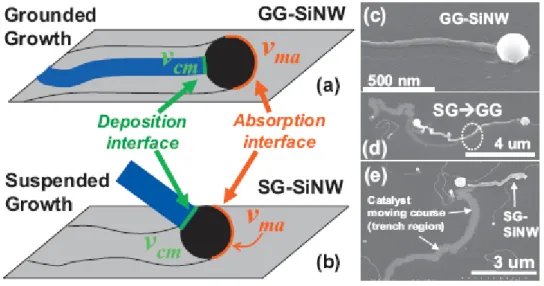
amorphous silicon (a-Si:H) matrix, which consumes and transfers a-Si:H into crystalline SiNW during the annealing process. Two different growth modes for the IPSLS SiNWs were found: the GG (grounded-growth) in which the produced SiNWs are attached to the substrate surface and the SG (suspended-growth) in which the produced SiNWs are suspended and carried by the catalyst droplet during its movement (figure 8). The authors have found that the diameter and the growth rate of SiNWs are proportional to the diameter of the catalyst droplet. They have also demonstrated three different methods to guide the growth of SiNWs in an in-plane surface.
Figure 8: Schematic illustrations of the two different growth modes for the growth of IPSLS SiNWs: (a) the GG mode and (b) the SG mode. (c) and (e) present the corresponding SEM pictures of the GG-SiNWs and SG-GG-SiNWs, respectively. (d) A transient case, from the initial SG mode to the final GG mode during the growth [11].
II.2.2 Porous template method
The objective of this method is to synthesize oriented nanowires with uniform diameter by using template (for example, the anodic aluminum oxide (AAO) or porous anodic alumina (PAA)) [12-14].
19
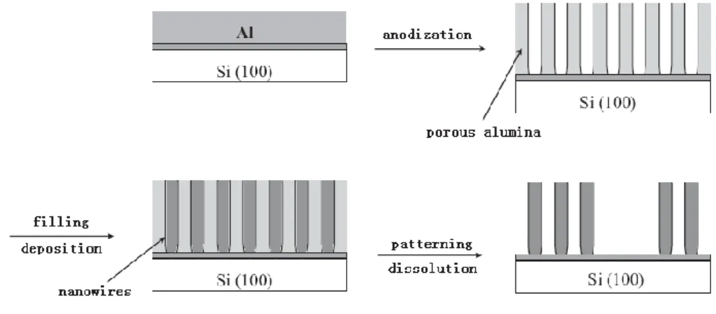
Figure 9: Schematic representation of the PAA films fabrication and nanowire arrays on silicon wafer. Figure 9 is a schematic representation of this method. The main procedure is divided into three steps. The first step is to fabricate an ordered porous anodic alumina film on the substrate. The diameter and the length of the nanopores can be controlled from a few nanometers to several hundred nanometers and several micrometers, respectively. The second step is to fill the pores of the template with certain materials which could be silicon or metal materials. The filling step can be achieved through different ways: electrochemical, high-pressure injection or evaporation. In addition, the VLS growth method is also commonly used to fill the porous network (figure 10). The last step is to remove the template via selective chemical etching. After the separation or dissolution of the template, a high density array of nanowires would be obtained.
Figure 10: a) Schematic cross-sectional drawing of the growth of Si nanowires in AAO nanopores using VLS method. b) Top-view SEM image of Si nanowires after selective etching of the AAO template. c) Cross-sectional TEM image of lower part of the Si nanowire in the AAO template [12].
State-of-the-art of silicon nanowires synthesis
20
II.2.3 Vapor-Liquid-Solid growth method
The name Vapor-Liquid-Solid (VLS) refers to the fact that the precursor in the vapor phase passes through a liquid droplet and finally ends up as a solid. A metal catalytic film is introduced into the reactor to form liquid droplets on the substrate surface. These droplets can adsorb a vapor to achieve the supersaturation at the back interface of the nano-droplets inducing growth of the nanowires on the substrate surface, usually in a three-dimensional (3D) configuration.
Otherwise, this technique permits doping the nanowires via simultaneously introducing some certain doping gas (the phosphine for N-type doping and the diborane for P-type doping) with precursor gas during the growth process. The most popular technique we use today is Chemical Vapor Deposition (CVD). The involvement of doping changes the conducting property of nanowires which enables the nanowires be integrated in many devices such as FET (Field Effect Transistor), biosensors, solar cells …
The studies of feasibility and sensitivity to certain gas will be demonstrated in this thesis by fabricating an electronic resistor gas sensor based on nanowires via VLS technique using Low Pressure Chemical Vapor Deposition (LPCVD) [15, 16]. And recently we have succeeded in doping the N-type nanowires in different doping concentrations which is rarely cited in the literatures. The details about the LPCVD-VLS growth and doping method will be introduced in chapter 3.
III VLS mechanism
The VLS mechanism was firstly proposed by Wagner and Ellis in 1964 [17, 18]. Two important phenomena were observed during the silicon wires growth process: an impurity is essential for the growth and a small droplet is present at the tip of the silicon wires. Therefore, they deduced that the role of the metal impurity including Au, Ag, Pt, Al… is to form a liquid droplet with relatively low temperature. The liquid droplet is a preferred site for deposition of silicon induced by the supersaturation of the alloy droplet from the vapor source (precursor gas). Up to now the VLS is still a key and popular mechanism for silicon nanowires growth. However, much smaller metal clusters (nanoclusters) are employed as catalysts for realizing
21
SiNWs because the initial size of the metal droplets will define the diameter of the SiNWs which varies from tens of nanometers to several microns [19]. In the process, the metal nanoclusters are heated above the eutectic temperature, for example, gold whose eutectic temperature is 363°C. Small Au-Si alloy droplets will form on the substrate surface. When the substrates are exposed in the precursor gas, such as silicon tetrachloride (SiCl4), silane (SiH4)
or disilane (Si2H6), precursor molecules will crack on the surface of the Au-Si alloy droplets
and meanwhile the silicon source decomposed from precursor gas is incorporated into the droplets. The sufficient Si incorporation results in the supersaturation of the alloy droplets which leads to a nucleation of the solid silicon. The continuation of this process realizes the synthesis of SiNWs with the alloy droplets riding on the tops (figure 11).
Figure 11: a) A schematic of the Au–Si binary phase diagram (PD); b) A schematic of silicon nanowire growth (using gold as catalyst) [7].
III.1 Gold as catalyst
In the VLS growth process, a lot of metals have been reported as catalysts including Au, Fe, Ag, Zn and so on [17, 20, 21]. However, gold is always the most frequently used metal catalyst material because it has so many interesting advantages listed below:
- Availability. Gold is widely used for electrical contacts and the machine equipped for depositing a thin film, for example evaporation system, is also easily found in most semiconductor research center.
- Nontoxic that means few safety requirements is needed.
460
State-of-the-art of silicon nanowires synthesis
22
- High chemical stability. It is barely oxidized in air.
- Relatively low eutectic temperature while high Si solubility. The eutectic point of Au-Si is at a concentration of 19% Si and at the temperature of 363°C which is much lower than the melting temperature of pure Au or pure Si.
- Low vapor pressure at high temperature. This feature avoids an unwanted evaporation of gold.
Although gold has such a lot of impressive advantages, one serious drawback is that it is known as impurity in nanowire which restricts its compatibility in semiconductor electronic production standards.
III.2 Generation of gold particles
Gold, as the widely used and well controlled metal catalyst in VLS mechanism, can be generated and deposited by various methods, including thermal evaporation, sputtering deposition, electron beam evaporation, colloidal gold, laser ablation… [22]. Their common objective is to realize appropriate nano gold particles whose size, position, surface density and cleanliness requirements are satisfied as the catalyst, which supports the subsequent VLS growth process. Here, we introduce two mostly used methods for generating gold nano particles:
1) Thin film annealing: The particles generated from thin film annealing method begin from a thin film deposition of gold on the substrate prepared by thermal evaporation system or sputter systems. The thickness of the thin film ranges from several nanometers to tens of nanometers. Then, the substrate with gold film will be transferred into the reactor chamber where the gold thin film will split up into gold particles during an annealing step up to 600°C for several minutes. The particles size depends mainly on the thickness of the catalyst film deposited [23]. A relatively long annealing time (20-30 minutes) allows for more homogeneous droplets spreading on the substrate [24]. It supplies us a simple, low cost and high throughput gold deposition method, however, the difficulties exist in the control of position, diameter and density controls.
23
Figure 12: (a) Schematically illustrating the size-controlled synthesis of SiNWs from Au-nanoclusters. (b) AFM image of 10 nm Au-nanoclusters dispersed on the substrate (top). Field Emission Scanning Electron Microscopy (FESEM) image of SiNWs grown from the 10 nm nanoclusters (bottom). The sizes of both images are 4µm. The inset in the bottom image is a TEM micrograph of a 20.6-nm-diam SiNW with a gold catalyst at the end. The scale bar is 20 nm. (c-f) Histograms of SiNW diameters grown from 5-, 10-, 20-, and 30-nm-diam Au-nanoclusters [19].
2) Colloidal gold particle deposition: Colloid particles (colloidal solution) with well defined gold diameters (2 nm to 30 nm) are commercially available and do not suffer from the same diameter controllability problems as in the thin film annealing method. The substrate is prepared via spin-coating using a negatively charged droplet of colloidal solution on a positively charged layer made up of a 0.1 % poly-L-lysine (PLL) solution which ensures the adhesion of the gold particles to the substrate by electrostatic interactions [25]. Using this method, Y. Cui et al [19] succeeded in obtaining 5-, 10-, 20- and 30-nm-diam Au-nanoclusters and nanowires with average 6.4-, 12.3-, 20-, and 31.3-nm-diam were fabricated respectively, which demonstrated that the size of the metal catalysts determines the diameter of the formed nanowires (figure 12). This method has improved a lot in
State-of-the-art of silicon nanowires synthesis
24
the problem of diameter controllability, but its position control is not solved as well as thin film annealing method. In addition, it brings us a new contamination problem induced by PLL.
III.3 Chemical Vapor Deposition
In VLS-based nanowires growth, many different growth methods have been used, including laser ablation [21], molecular beam epitaxy (MBE) [26] and Chemical Vapor Deposition (CVD). The most popular method for growing silicon nanowires is CVD that generates the gaseous semiconductor reactant source by the decomposition of precursor gas such as silane (SiH4) [27, 28], disilane (Si2H6) [29], silicon tetrachloride (SiCl4) [17, 30, 31].
This decomposition process can be obtained either by plasma (PECVD) or thermal energy (APCVD, LPCVD…). The decomposed Si molecules will be transported into the catalyst droplets and cracked into its constituents (figure 13).
Figure 13: Schematic of experimental setups for silicon nanowires growth by CVD [17].
Advantages of CVD nanowires growth:
- The length and diameter configurations of nanowires growth can be controlled. (Such configurations of NWs realized by LPCVD will be discussed in chapter 2.) - Offering an opportunity of a well-controlled doping by intentionally employing
additional doping precursor at the same time as the silane precursor gas, so called “in-situ doping”, and additional step for doping is not needed.
25 Drawbacks of CVD growth of nanowires:
- The silicon nanowires grown by CVD exhibit a certain variation of the growth direction [32, 33].
- The precursor gases, doping gases and the reaction products are often toxic and explosive which requires strict safety consideration.
III.4 In-situ doping for silicon nanowires
One of the main reasons that make silicon nanowire superior to carbon nanotube is the possibility of better controlling the conductivity and carrier type by adding impurities. Silicon nanowires are generally doped by pentavalent elements (P, As, Sb…) to conduct with negative electrons (n-type) or trivalent elements (B, In…) to conduct with positive holes (p-type). This creates a number of potential applications for silicon nanowires such as field effect transistor (FET), biosensor, memory, solar cells…In-situ doping is such a good method that succeeds in doping the silicon nanowires. It injects the mixture of the dopant gas and the precursor gas into the reactor chamber at the same time which means the impurity atoms are being introduced into the crystal lattice in the silicon nanowires cores while the silicon nanowires are growing [34-36].
III.4.1 N-type doping by phosphine
The most familiar gas used for the n-type doping is phosphine (PH3) which is injected
at the same time with the silane during the growth of silicon nanowires. To avoid deposition of silicon everywhere on the substrate, the substrate coated with gold catalyst is heated to a lower temperature of precursor gas molecules cracking (approximately 500°C) under the precursor atmosphere (SiH4 combined with PH3), and meanwhile the decomposited gas-phase
phosphorus will be cracked into the Au-Si droplet to realize the doping. According to G. F. Zheng [34] and Y.F. Wang [37], they have demonstrated that phosphorous dopant concentration can be readily controlled by varying the ratio of PH3 and SiH4 ([P:Si]) grown on
a <111> oriented silicon substrate. Figure 14(a) shows a plot of SiNW resistivity and carrier type as a function of [P:Si]. Significantly, when the ratio [P:Si] is increased, the resistivity is
State-of-the-art of silicon nanowires synthesis
26
correspondingly decreased. They have also found out that the majority of the phosphorus-doped SiNWs imaged (figure 14 (b-c)) were single crystal with a 111 growth direction, a smaller fraction of SiNWs were bicrystals with a 112 growth direction and the homogeneous deposition of Si/P doesn’t occur during axial elongation (figure 15 (a-b)).
Figure 14: (a) Four-point resistivity of SiNWs grown using [B:Si]=2×10⁻², [P:Si]=0, 2×10⁻⁵, 7×10⁻⁵, 2×10⁻⁴ and 2×10⁻³; TEM images of phosphorus-doped SiNWs: (b) with [P:Si]=2×10⁻⁵,(c) with [P:Si]=2×10⁻³ [37].
Figure 15: (a) and (b) TEM images of two opposite ends of one 22 nm diameter SiNW; the scale bar is 5 nm [34].
27
III.4.2 P-type doping by diborane
Diborane (B2H6)is widely used as the p-type dopant gas [32, 33, 38, 39] while the
trimethylboron (TMB-C3H9B) is also used to synthesize silicon nanowires [33]. Compared
with n-type doping, p-type doping has been studied much more deeply because the experimental configurations will directly affect the morphology and the quality of the p-doped silicon nanowires. L. Pan et al [32] have studied the effect of diborane on the microstructure of SiNWs. Figures 16 (a-b) show us the SEM images of the lightly doped SiNWs using B2H6
as the doping gas, and figure 16 (c)-(e) show us two SEM and one TEM images of the highly doped SiNWs [32]. We can observe that the highly doped SiNWs are curved and kinked with an average length of approximately 8.5 µm (figure 16 (d)) and a shell of amorphous silicon is deposited outside of the doped nanowire (figure 16 (e)). This result is due to the low dissociation energy of B2H6 which is about 27 kcal/mol [40]. The B2H6 reacting with SiH4
leads to an increase in µSi growth which is believed to be responsible for the formation of the amorphous Si surrounding the B2H6-doped nanowires. K-K. Lew et al [33] have investigated
the use of TMB as p-type dopant gas and succeeded in doping the nanowires whose boron concentration measured can range from 1×10¹⁸ to 4×1019 cm-3 [figure 17(a)]. Figure 17(b) shows a High-Resolution Transmission Electron Microscopy (HRTEM) image of TMB-doped SiNW with [111] growth orientation [33]. The dissociation energy of TMB is approximately 87 kcal/mol which leads to an increased thermal stability compared with B2H6. This enables the
highly B-doped SiNWs by TMB without a thick amorphous Si coating.
Figure 16: (a-b) SEM images of the top view and cross-sectional view of the B2H6 lower-doped SiNWs; (c-d) SEM images of highly doped SiNWs; (e) Bright-field TEM image of a typical B2H6 highly doped SiNW, showing the core-shell structure. The inset is the corresponding diffraction pattern [32].
State-of-the-art of silicon nanowires synthesis
28
Figure 17: (a) Boron concentration in SiNWs obtained by secondary ion mass spectrometry (SIMS) measurements as a function of the [B:Si] ratio in the inlet gas.; (b) HRTEM image of TMB-doped SiNW with [111] growth orientation. A thin oxide layer was observed on the outer surface [33].
IV Electronic devices based on silicon nanowires
During the last half century, a drastic scale-down tendency of electronics has taken place, and the industry expects to continue the miniaturization for at least next ten years. Silicon nanowires are considered as such promising materials or components that they would have a great impact in the future CMOS technology. However, before massive integration into the technology, individual electronic device with excellent performance should be realized. Fortunately, a lot of amazing electronic devices based on silicon nanowires have already been realized such as vertical nanowire field effect transistors (NWFETs), logic gates, solar cells… Although a great number of potential applications are discovered, much further work should be carried out before achieving the mass production in semiconductor industry.
IV.1 Vertical nanowire FET
The use of nanowires in electronics enables new gate architectures for a transistor. An evolution of the field-effect-transistor is showed in figure 18. Their field effects differ from each other via different gates’ surrounding structures. Obviously, the vertical NWFET has a complete and uniform wrap-around effect which depletes the channel region and that will greatly improve the performance of the transistor.
29 Some advantages of such structures are:
- Conduction in the whole bulk of the nanowire, - No parasitic capacitance at the source/drain regions. - Low leakage current.
Figure 18: Field-effect-transistors, (a) MOSFET, (b) FinFET, (c) lateral NWFET, and (d) vertical NWFET [41].
Figure 19 and 20 show an example of a vertical nanowire transistor based on a 60-nm-diam, 2-µm-length silicon nanowire and its corresponding electrical characteristics. The vertical silicon nanowires are synthesized by VLS method. A 25-nm-thick SiO2 gate dielectric
is deposited around the nanowires and a 100-nm-thick aluminum is deposited as gate electrode. Subsequent optical lithography and wet etching will realize patterning of the gates. Finally, a top Ni contact is defined using resist as etching mask. The processing details can be acquired from the reference [42].
Figure 19: (a) 60-nm-diameter SiNW covered with 25 nm SiO2 gate dielectric, (b) SiNW with gate length defined by etching of Al, (c) schematics of the surround-gated transistor displaying the gate length LG and ungated regions L1 and L2 [42].
State-of-the-art of silicon nanowires synthesis
30
Figure 20: (a) output and (b) transfer characteristics of the vertical NWFET represented in figure 19 [42].
IV.2 Crossed silicon nanowire-based logic gates
The crossed nanowire (cNW) architecture [43] is a powerful strategy for memory and logic devices in which the key device features can be defined during the synthesis of nanowire building blocks and their subsequent assembly. Based on cNW structure, the most important elements for logic gates, diodes and transistors [44-46], can be fabricated. The electronic characteristics of the functional elements are achieved by the two crossed nanowires which could be a p-type nanowire and an n-type nanowire. An example of a crossed SiNW p-n junction is shown in figure 21 [44]. The crossed SiNW p-n junction is assembled from two 20 nm diameter p- and n-type SiNWs.
Figure 21: A) Typical Field Emission Scanning Electron Microscopy (FESEM) image of a crossed SiNW junction. The scale bar is 2 µm. B) The black and green curves correspond to the I-V behavior of individual p- and n-type SiNWs, respectively. The solid red line corresponds to voltage drop measured between 3 and 4, and the dashed red line to voltage between 3 and 2 [44].
31
Via the development of this assembly approach, a lot of crossbar devices can be easily fabricated, such as logic gates, decoders [47, 48]… Figure 22 shows a logic NOR gate realized by using a p-type silicon nanowire as channel unit and three n-type gallium nitride (GaN) nanowires as gates [45]. The single-crystal p-Si and n-GaN NWs are synthesized by nanocluster-catalyzed methods and have diameters of 10 to 25 and 10 to 30 nm, respectively.
Figure 22: a) Schematic of logic NOR gate constructed from a 1 p-type silicon nanowire by 3 crossed n-type GaN nanowires junction array. b) The output voltage versus the four possible logic address level inputs. c) The measured truth table for the NOR gate [45].
IV.3 Solar cells
With the industrial development, a large abundance of natural resources such like fossil fuel have been consumed. Therefore, the alternative renewable clean energy sources are severely in need for the future. Among various green natural energy sources, the solar energy is the most efficient and technologically potential. The energy from sunlight striking earth in an hour can meet the whole energy consumption by humans in an entire year. To make full use of solar energy, an efficient device that can capture, convert and store solar energy should be fabricated. Since the invention of Si solar cell 50 years ago [49], the Si photovoltaic solar cell devices remain the basis of the solar energy converters due to the abundance of silicon materials and the high reliability and high efficiency of silicon photovoltaic devices. Recently, the progressive developments in nanotechnology make SiNWs photovoltaic devices [50-54] become a promising candidate for building photovoltaic devices because of the following advantages:
State-of-the-art of silicon nanowires synthesis
32
- Simple and low-cost fabrication of large-area dense arrays of SiNWs (for example, via VLS method).
- The as-prepared SiNWs don’t peel of the substrate since the as-prepared SiNWs are an integral part of the Si wafer substrate.
- The rough surfaces of the SiNWs enable almost nonreflective property due to strong light scattering and absorption.
- Good compatibility with other current Si-based microelectronics.
Here, figure 23 shows us a photovoltaic device based on a single p-type/intrinsic/n-type (p-i-n) coaxial SiNW [54]. In the radial p-n junction geometry, the single nanowire synthesized by VLS-CVD method consists of a p-type SiNW encased in intrinsic polycrystalline silicon with a further layer of n-type polycrystalline silicon. When the single p-i-n coaxial SiNW is exposed to the sunlight, the photo-carriers absorbed along the SiNW will be transferred through the short travel distances between the absorbing surfaces to the collection electrodes. An overall power conversion efficiency of 3.4% has been achieved by this solar cell which can serve as robust power sources.
Figure 23: Schematics of a single p-i-n coaxial SiNW solar cell and corresponding SEM images [54].
IV.4 Silicon nanowire sensors
Besides the above mentioned applications of SiNWs, devices based on silicon nanowires have many other important and promising applications especially as sensors.
33
Taking advantage of their small size, giant piezoresistance and large surface-to-volume ratio properties, SiNWs can be developed for various applications as sensors, such as mechanical sensors, biosensors and gas sensors… These sensors are mostly based on the transistor principle, especially field-effect transistors. The details about the mechanisms, assembly technologies and working performance will be introduced in chapter 2.
V Conclusion
In this chapter, the nanowire growth strategies and some growth methods are firstly introduced to help us to understand the main synthesis methods. Then, the key VLS mechanism of synthesizing our NWs is explained in detail. Catalysts, reactors and doping methods are discussed, which will directly affect the quality of silicon nanowires.
In fact, the objective in our work is to realize reasonable doping concentrations and the subsequent characteristics as a sensor.
The objective of this research work is to realize microelectronic silicon nanowires based devices synthesized via the Au-catalyst VLS method. The objective of this work is to study the potential applications of these devices as chemical sensors with high sensitivity.
34
Chapter II
35
I Introduction
Rapid progress in materials science and nano technologies has led to the development of electrical devices whose working performance has partially achieved specific detection functions (mechanical, electrical…) and biochemical diagnosis functions as well as human’s components of organs or live cells. Today’s visual technologies have already surpassed the capability of the human brain in many aspects. However, some functions of the human like olfactory system has not been achieved yet. The conventional sensors may hold some of these gas sensing problems and recently-developed nanoscale sensors based on nanowires provide a wider range of applications in pressure measuring, explosive detection, clinical assaying, working environment hazard monitoring…
The conventional biochemical sensors realize their function via adsorption of target molecules and changing the electronic states of the atoms at the reacting surface. The electrical transport characteristics will be changed directly. Most popular form of sensors is transistor which has been used to detect different analytes, because the gate effect of the transistors can increase the modulation of the channel conduction. Top suspended gate and back gate are usually used in order to avoid encapsulating the reacting surface and ensure the reacting surface having direct contact with the analytes. When a gate voltage is applied, the gate voltage will enhance or reduce the molecule adsorption on the transistor surface [55, 56, 57].
Nanoscale sensors based on nanowires used as sensitive unit follow nearly the same principle as the conventional sensors. However, they are expected to be more promising and have more significantly enhanced performance due to the following advantages:
1) Small size with dimensions on the sub-100 nm scale. The interacting biological molecules and other species of interest are also at the nanometer size scale which improves the selectivity of the sensors.
2) Large surface-to-volume ratio of one-dimensional nanowires which provides high-efficiency surface modification and then increases the sensitivity of the sensors when compared to a conventional sensor.
3) The specific properties of SiNWs like giant piezoresistivity and thermal electricity enable sensors based on silicon nanowires to transform many environmental
State-of-the-art of silicon nanowires based sensors
36
quantities (slight deformation, a thermal signal…) to an electrical signal with relatively high sensitivity and low power consumption.
The synthesis methods for silicon nanowires have been introduced in the previous chapter. However, for sensors based on these nanowires, the assembly modes are much more important. In order to realize the functions of sensors, the nanowires should be widely opened (noncapsulated) when the sensors are exposed to the sensing targets or modified by bioaffinitive agents. There are two most commonly used sensor structures. The first one is single nanowire sensor (figure 24). The single nanowire is the only transmission channel between the two electrodes. This kind of sensor can be fabricated by many different ways (pick-and-place approach [35, 58], the superlattice nanowire pattern transfer (SNAP) approach [59] and so on) whose objective is to locate a single nanowire on a certain position. The metal electrodes could be pre-patterned on the substrate before placing the nanowire or be defined at both ends of the single nanowire after. However, in most cases, due to the difficulty with precise positioning, size control and self orientation (especially in planar configuration) of the silicon nanowires after synthesis, post positioning methods are usually used for addressing silicon nanowires. Although these methods are feasible to realize the single nanowire sensor, the drawbacks such as device-to-device non-uniformity, time-consuming and unsuitable for large-scale manufacturing, are evident.
Figure 24: a schematic of a single nanowire sensor.
The second sensor structure is based on bundles (carpet) of nanowires (figure 25) and is generally used as a resistive nanowires sensor. The electrical conduction between source and drain is transferred through the whole nanowires network. The electrodes can be interdigitated to increase the active sensor area and the separation of the electrodes can be longer than the single nanowire sensor (see chapter 3). Nanowires electrical addressing does
37
not need additional transfer step for nanowires. In this case, the bundles of nanowires can be prepared directly on the substrate by most of main synthesis methods like VLS or SLS.
Figure 25: a schematic of a carpet nanowires sensor.
Compared with the single nanowire sensor, the fabrication method of the bundles of nanowires sensor is much easier and more efficient, but the response speed becomes slower because of the longer transmission distance.
II Silicon nanowires based mechanical sensors
Since 1954, C.S. Smith et al. have studied the various effects of strain on silicon [60]. It is recognized that the resistance changes not only due to the change in geometry but also due to the resistivity of the material. The piezoresistive effect of semiconductor materials can be several orders of magnitudes larger than the geometrical effect in metals. So semiconductor materials, and in particular silicon, can be used to create a sensitive mechanical sensor and almost every semiconductor manufacturer has announced their version of strained CMOS [61].
Recently, with the rapid development of nano technology, the silicon nanowire has been studied experimentally and theoretically as a particular attractive candidate material to realize nanoelectromechanical systems (NEMS). R. He and P. Yang [62, 63] have reported that silicon nanowires possess an unusually large piezoresistance effect compared with bulk. The relationship between conductivity/resistivity and stress/strain is given by:
State-of-the-art of silicon nanowires based sensors
38
where σ0 is the conductivity under zero stress and X is the stress. The longitudinal
piezoresistance coefficient [64] along the <111> direction for p-type Si nanowires can reach 37 times larger than the piezoresistance coefficient for bulk. Such giant piezoresistance effect in silicon nanowires can be used to realize a more efficient sensitive nano-mechanical sensor.
Figure 26-(a) shows a nano-mechanical sensor based on one single nanowire [62, 63]. Most of such single nanowire-based devices are fabricated by the pick-and-place approach to realize FETs and chemical sensors. Here, the suspended 2 µm length p-type Si nanowires have been grown laterally via gold catalyst VLS-CVD method. Si nanowires grow preferentially along <111> direction from vertical <111>-oriented faces pre-patterned microtrenches on a <110>-oriented SOI substrate (figure 26-(b)). The advantages of this method over the pick-and-place approach are that the nanowire synthesis and device fabrication can be achieved simultaneously, and the length of nanowires can be well controlled during the self-assembly process. When the nanowires were over grown, which means the length of the nanowires exceeded the widths of the trenches, a self-welding connection was achieved. As shown in figure 26-(b), the backward growth of nanowire directly indicates that nanowire should be self-welded with the opposite sidewalls and should form solid connections, which is very important for a mechanical sensor to avoid the fracture between the nanowires and the sidewalls.
Figure 26: (a) SEM image of a <111>-oriented nanowire grown in trench on <110>-oriented silicon-on-insulator (SOI) wafer, (b) an enlarged image of the bridged nanowire which finally grew backwards after self-welding into the sidewall. The scale bars in (a) and (b) are 2 µm and 500 nm, respectively [63].
39
Uniaxial stresses were applied on Si nanowire along its length by the four-point bending method. A schematic for the four-point bending setup is shown in figure 27-(a) and the details about the method can be acquired in reference [65]. The I-V characteristics curves (figure 27-(b)) and the uniaxial stresses were performed simultaneously. The conductance of the nanowire (70 nm × 1.2 µm) increases under compressive stresses and decreases under tensile stresses. Relative changes in conductivity for this nanowire can be calculated from the curves of figure 27-(b) and the piezoresistance coefficient can be deduced according to the equation (1) at the same time. The relationships between and stress X
Figure 27: (a) Schematic diagram for the four-point bending setup; (b) I-V characteristics curves of a p-type <111>-oriented nanowire (70 nm × 1.2 µm) under compressive and tensile stresses; (c) Relationships between the relative change in conductivity and stress/longitudinal strain. Four types of nonlinear behaviours of nanowires are shown, labeled with letters I, C, L and Z. The inset shows the overview for L. (d) First-order longitudinal piezoresistance coefficient of p-type Si nanowires and its dependence on diameter and resistivity [63].
State-of-the-art of silicon nanowires based sensors
40
and the statistical piezoresistance coefficients
,
from nanowires with different diameters and resistivities, including bulk Si whose resistivity is 1 Ω·cm as reference, were plotted in figures 27-(c) and (d).The for p-type Si nanowires can reach as high as -3,550×10-11Pa-1, while the piezoresistance coefficient for bulk has only -94×10-11Pa-1. They have deduced that the piezoresistance coefficient increases with decreasing nanowire doping level and diameter of the nanowire. Thanks to the 1-D nano-structure and the giant piezoresistance coefficient, p-type <111>-oriented Si nanowires enable many applications in flexible electronics and nanoelectromechanical systems. Compared with bulk Si or conventional mechanical sensor, the SiNW sensor is more sensitive and has more efficient performances.
III Silicon nanowires based chemical and biological sensors
Today, chemical or biological sensors are widely used in many domains such as medicine, diet, environmental security… But at the same time, the requirements on the sensors become more and more strict. Thanks to their high surface area to volume ratio and diameters comparable to those of the chemical and biological species being sensed, the 1-D nanowires can be used as nano sensors with a high sensitivity in both chemical and biological domains. The details about the mechanisms, assembly technologies and working performance for different sensors will be presented in the following sections.
III.1 Silicon nanowires based gas sensors
Silicon gas sensors are very attractive because of their interesting properties such as high sensitivity, compatibility with classical silicon technology, low cost and low power consumption. They are usually used for detecting the oxidizing gas like nitrogen dioxide (NO2) and the reducing gas like ammonia (NH3). The detection of NO2 is important for
monitoring environmental pollution resulted from automotive emissions [66] and the detection of NH3 is needed in industrial and medical environments [67]. Recently, the SiNW
41
and more popular than silicon film gas sensors, because their surface conductivity and surface potential are easier to be affected due to the large surface to volume ratio.
III.1.1 Suspended Gate Field Effect Transistor gas sensor
Previous studies in DM2-IETR have demonstrated a successful suspended-gate field effect transistor (SGFET) which has application in gas detection. The structure of the SGFET is shown in figure 28 [71]. The key steps of the procedure are introduced briefly as below. A layer of undoped polycrystalline silicon and a layer of heavily doped polycrystalline silicon are etched successively to define channel zone, source and drain regions, respectively. Then, a 500 nm thick sacrificial layer of germanium is deposited and patterned to form the bridge anchors. The thickness of the sacrificial layer is the exact height of the air-gap. After definition of gate, source and drain contacts, the last step is to remove the sacrificial layer via wet etching using hydrogen peroxide (H2O2).
Figure 28: (a) A 3-D schematic of an SGFET, (b) SEM image of a top view for SGFET [71].
The transfer characteristic of SGFET under NO2 and NH3 are shown in figure 29 and
30. Before exposure to NO2 at 10% relative humidity (RH), the reference curves are measured
in air with the same conditions. We can observe that the Ion decreases systematically as a
result of the introduction of NO2 (figure 29-(a)), because the molecules of NO2 act as acceptor
centers (known as oxidizing agent [72]) and create negative ions NO2-. Once these ions have
been adsorbed on silicon surface, the free carriers (electrons) concentration in silicon would be decreased. In other words, negative ions NO2- adsorbed on the surface of active layer
State-of-the-art of silicon nanowires based sensors
42
(channel zone) act as negative charges -Qss in gate insulator, thus explaining threshold voltage
increasing for N-type channel transistor (figure 29-(b)).
Figure 29: (a) Transfer characteristics of N-type SGFET under different NO2 contents in parts-per-million (ppm) at 10% relative humidity (RH) synthetic air, (b) Negative charges -Qss due to NO2 adsorption on channel surface [71].
Contrary to NO2 effect, the NH3 effect is exactly inverse (figure 30). The reducing
character of NH3 leads to the negative shift of the threshold voltage. Indeed, the molecules of
ammonia act as donor centers (reducing agent). Once they have been adsorbed on silicon surface, positive ions NH3+ act as positive charges +Qss thus explaining threshold voltage
decreasing.
Figure 30: (a) Transfer characteristics of N-type SGFET under different NH3 content in ppm or under dry synthetic air, (b) Positive charges +Qss due to NH3 adsorption on channel surface [71].
43
The threshold voltage Vth of SGFET can be expressed by:
(2)
where is the difference between the work functions of the gate material and the semiconductor, the Fermi level position in the semiconductor versus the mid-gap, the space-charge in the semiconductor, C the total capacitance between the gate material and the semiconductor, the thickness of the insulator, is the charge in the insulator at a distance of from the gate, is the charges on the surface of active layer (channel zone) which is equal to . Usually only the last variation is considered in this SGFET which influences the final , because the charges in the ambience directly lead to the variation of in case of a high field due to a very low gap. This property enables the SGFET being used as an excellent gas sensor.
III.1.2 Silicon nanowires gas sensors
Researchers have made great efforts to develop a gas sensor which can sense gases (for example, NOx) at room temperature for a long time. In the last few decades, one of the
most important gas sensors is made of metal oxides (ZnO, In2O3…) [73-75]. However, the
metal oxide based sensors can generally only be operated above 200°C [66, 76]. So, a sensor based on other materials should be realized to achieve the detection function at room temperature. In particular, silicon nanowire is just such material that could be used because it is a highly resistive material for exchanging with oxidizing and reducing gases at room temperature.
III.1.2.1 NO
2effect
J.R. Heath et al. [59, 77, 78] have realized a gas sensor based on SiNW arrays on flexible plastics, which is suitable for sensing gaseous nitrogen oxide (NO2) at room
![Figure 3: Cross sectional SEM images of silicon nanowires realized by T-NIL [4].](https://thumb-eu.123doks.com/thumbv2/123doknet/7935267.265822/15.892.158.739.295.509/figure-cross-sectional-sem-images-silicon-nanowires-realized.webp)

![Figure 23: Schematics of a single p-i-n coaxial SiNW solar cell and corresponding SEM images [54]](https://thumb-eu.123doks.com/thumbv2/123doknet/7935267.265822/33.892.172.713.606.903/figure-schematics-single-coaxial-sinw-solar-corresponding-images.webp)
![Figure 31: Schematic of the SiNWs arrays NO 2 gas sensor and the measuring installation [78]](https://thumb-eu.123doks.com/thumbv2/123doknet/7935267.265822/45.892.194.698.321.620/figure-schematic-sinws-arrays-gas-sensor-measuring-installation.webp)


![Applications de la Chimie Radicalaire des Xanthates : Synthèse d'Alcaloïdes d'Origine Marine ; Synthèse de Thiéno[2,3-b]thiopyranones ; Synthèse de Thioéthers Aryliques ; Approche à la Synthèse Totale du (+)-Maritimol.](data:image/gif;base64,R0lGODlhAQABAIAAAP///wAAACH5BAEAAAAALAAAAAABAAEAAAICRAEAOw==)