UNIVERSITÉ DE MONTRÉAL
HIGH-ACCURACY DIGITAL TO ANALOG CONVERTER DEDICATED TO
SINE-WAVEFORM GENERATOR FOR AVIONIC APPLICATIONS
MASOOD KARIMIAN-SICHANY DÉPARTEMENT DE GÉNIE ÉLECTRIQUE ÉCOLE POLYTECHNIQUE DE MONTRÉAL
MÉMOIRE PRÉSENTÉ EN VUE DE L’OBTENTION DU DIPLÔME DE MAÎTRISE ÈS SCIENCES APPLIQUÉES
(GÉNIE ÉLECTRIQUE) MAI 2013
UNIVERSITÉ DE MONTRÉAL
ÉCOLE POLYTECHNIQUE DE MONTRÉAL
Ce mémoire intitulé:
HIGH-ACCURACY DIGITAL TO ANALOG CONVERTER DEDICATED TO
SINE-WAVEFORM GENERATOR FOR AVIONIC APPLICATIONS
présenté par : KARIMIAN-SICHANY Masood
en vue de l’obtention du diplôme de : Maîtrise ès Sciences Appliquées a été dûment accepté par le jury d’examen constitué de :
M. SAVARIA Yvon, Ph.D., président
M. SAWAN Mohamad, Ph.D., membre et directeur de recherche M. THIBEAULT Claude, Ph.D., membre
DEDICATION
To my mother,
for her inimitable love and patience
ACKNOWLEDGEMENTS
I give my deepest thanks to God who guides me in such a wonderful way, instructs me whatever I understand, and helps me through inspiring people with whom I grow. Among those people, I am always thankful to my parents for their love and devotion. I cherish them.
It has been my honor to study and work in Montreal Polytechnique and Polystim laboratory. I would like to express my appreciation and respect to my supervisor, Professor Mohamad Sawan for his continuous support, guidance, and encouragement. This Master thesis could never have been completed without his help and advice.
I am also grateful to the members of the examining board of my Master thesis, Prof. Yvon Savaria and Prof. Claude Thibeault, for their feedbacks on this Master thesis and also on my progress in AVIO402 project during all these years.
During my program, I have been supported by postdoctoral fellows of Polystim laboratory. I would like to acknowledge Dr. Ali Naderi who technically supported and contributed in this work. My gratitude also goes to Dr. Saeid Hashemi for his invaluable help and encouragement. Moreover, I wish to thank Mrs. Marie-Yannick Laplante for her office support, Réjean Lepage for network and software administration, and all other students and technicians of Polystim, in particular Mona Safi-Harb, Amine Miled, Guillaume Simard, Faycal Mounaim, Sami Hached, Genevieve Massicotte, and Laurent Mouden for their support and providing friendly environment. I am sincerely grateful to my friend, Madjid Mokhtari, for his encouragement and heartfelt friendship.
I am truly indebted to my undergraduate teacher, Professor Saeid Sadri, and I would like to express my special thanks to him for his prodigious influence on my understanding methodology. I would like to acknowledge financial support from Natural Sciences and Engineering Research Council of Canada (NSERC), Bombardier aerospace, Thales Canada Inc., MITACS, Consortium for Research and Innovation in Aerospace in Quebec (CRIAQ), and the products and services provided by Canadian Microelectronic Corporation, and Polystim neurotechnologies laboratory. Last but not least, I want to thank my wife and my son for their being with me, support, and sacrifice during all these years.
RÉSUMÉ
De nos jours, malgré les avancées remarquables de la microélectronique, les systèmes avioniques emploient essentiellement des technologies vieillissantes afin de répondre aux normes de sécurité exigeantes des systèmes avioniques. La nouvelle génération d'avionique modulaire intégrée (AMI) des More Electric Aircrafts (MEA), nécessite des architectures de réseaux stables et fiables, employant des modules électroniques intégrables modernes qui restent à être conçus et développés. Suivant cette tendance, une interface générique intelligente pour capteurs (Smart Sensor Interface - SSI), dédiée aux capteurs de position avionique est proposée dans ce mémoire. Le circuit intégré SSI fera partie d'un réseau de capteurs AFDX amélioré et est composé de signaux d'excitation et de modules d'acquisition de données. Les efforts de conception sont concentrés sur l'unité de génération de signaux d'excitation (Excitation Signal Generation - ESG) de la SSI.
En tant que lien entre le réseau AFDX et les capteurs de déplacement, l'unité ESG doit générer des signaux sinusoïdaux précis, d'une fréquence allant de 1.5 kHz à 10 kHz. En respectant la programmation de l'interface, nous démontrerons qu'une architecture de générateur de signaux basée sur la mémoire est la seule option qui réponde aux objectifs du design.
Le design d'un convertisseur numérique-analogique (CNA) basé sur le principe du sur-échantillonnage et faisant partie du chemin ESG est également présenté dans ce travail. Ce CNA est le noyau d'un générateur de signaux sinusoïdaux versatile conçu pour le système SSI proposé. Un taux d'échantillonnage élevé est utilisé dans ce CNA, de façon à obtenir un rapport signal sur bruit (Signal to Noise Ratio - SNR) élevé. Une analyse de l'impact d'une implémentation carrée et non-carrée de la matrice de sources de courant (Current Source Array - CSA) sur la performance de la séquence de commutation est présentée. Il sera démontré que la considération de tels impacts conduit à la conception de CNA plus précis. Une séquence de commutation optimale pour la taille du CSA conçu, sera introduite. Afin de réduire la taille des plots d'entrées et de sorties de la puce, un convertisseur de données série à parallèle haute-vitesse est inclu dans le CNA. Ainsi, les données d'entrée peuvent être envoyées de façon sérielle à un registre à décalage et appliquées de façon interne au noyau du CNA. Le CNA a été fabriqué sur une puce d'une dimension de 1.2 × 1.2 mm2 fabriqué avec la technologie IBM CMOS 0.13µm et est alimenté
avec une tension de 1.2 V. Générant un courant d'onde sinusoïdale ayant une valeur crête de 1023 µA, le CNA proposé permet d'obtenir un SNR plus élevé que 84 dB dans la bande passante Nyquist DC à 20 kHz.
ABSTRACT
Today, despite the astonishing advances in the field of Microelectronics, avionics systems are mostly employing older technologies to guarantee the level of reliability required by stringent safety standards of avionic systems. Toward the new generation of Integrated Modular Avionics (IMA) in More Electric Aircrafts (MEA), reliable and stable network architecture which employs modern integrated electronic modules must be designed and developed. In this trend, a generic Smart Sensor Interface (SSI) for avionics displacement sensors will be proposed in this Master thesis. The integrated SSI circuit will be part of an improved AFDX sensor network and consists of signal excitation and data acquisition paths. The design efforts of this Master thesis will focus on the Excitation Signal Generation (ESG) unit of the SSI.
As a link between AFDX network and displacement sensors, the ESG unit should generate pure and accurate sine-waveform with variable frequency between 1.5 kHz and 10 kHz. Respecting the programmability of the interface, it will be shown that a memory-based signal generator architecture is the only choice which supports the design objectives.
As part of the ESG path, the detailed design of a 10-bit interpolating digital to analog converter (DAC) will also be presented in this work. The DAC is the core of a versatile sine-waveform generator unit designed for avionics SSI. High-speed sample rate will be used in this segmented current steering DAC in order to achieve a high Signal to Noise Ratio (SNR). In the module level design of the DAC, the impact of square and non-square implementation of the current source array (CSA) on the performance of the switching sequence is introduced. It will be shown that considering such impacts will lead to the design of more accurate DACs. An optimum switching sequence for the designed CSA size will be designed and introduced. In order to reduce the I/O pads of the chip, high-speed serial to parallel converter will be included in the DAC. Thus the input data can be serially sent to the input shift register and internally applied to the DAC core. The DAC was fabricated on 1.2 × 1.2 mm2 chip fabricated using IBM 0.13µm CMOS technology, operating with a supply voltage of 1.2 V. Sourcing a sine wave current with a peak of 1023 µA, the proposed DAC is able to achieve a SNR better than 84 dB in the Nyquist bandwidth of DC to 20 kHz.
TABLE OF CONTENTS
DEDICATION ... III ACKNOWLEDGEMENTS ... IV RÉSUMÉ ... V ABSTRACT ... VII TABLE OF CONTENTS ... VIII LIST OF TABLES ... X LIST OF FIGURES ... XI LIST OF ABBREVIATIONS AND SYMBOLS ... XIV
CHAPTER 1 INTRODUCTION ... 1
1.1 Project overview ... 1
1.1.1 Sensor/network interfaces and new position sensors ... 3
1.1.2 Safety-critical avionics data network ... 3
1.1.3 Frequency selection for safety-critical wireless communication systems ... 4
1.1.4 Project organization ... 4
1.2 Motivation ... 6
1.3 Basic principles of displacement sensors ... 8
1.3.1 LVDT and RVDT inductive sensors ... 9
1.3.2 LVDT and RVDT interfacing ... 10
1.4 Research objectives and challenges ... 12
1.5 Contributions ... 13
1.6 Thesis outline ... 14
CHAPTER 2 BACKGROUND ON EXCITATION SIGNAL GENERATION AND R/LVDT INTERFACING 15 2.1 Introduction ... 15
2.2 Integrated sensing systems ... 15
2.3 L/RVDT integrated interfacing ... 17
2.4 Sine wave generation methods ... 22
2.5 Digital to Analog converter architectures ... 24
2.5.1 State of the art of current-steering DACs ... 28
2.6 Conclusion ... 30
CHAPTER 3 THE ESG ARCHITECTURE AND DAC DESIGN ... 31
3.2 The ESG requirements and block diagram ... 32
3.2.1 ESG design requirements ... 32
3.2.2 Proposed ESG block diagram ... 34
3.3 The CSDAC architecture, specifications, and design procedure ... 39
3.4 CSDAC design phase ... 43
3.4.1 Architectural design ... 45
3.4.2 Module design ... 49
3.4.3 Circuit design ... 56
3.4.4 Layout design ... 60
3.5 Conclusion ... 61
CHAPTER 4 SIMULATION AND MEASUREMENT RESULTS ... 62
4.1 Introduction ... 62
4.2 DAC testing techniques ... 62
4.2.1 Static specification measurement ... 63
4.2.2 Dynamic specification measurement ... 65
4.2.3 Simulation result characterization ... 67
4.3 Simulation results ... 68
4.3.1 Transistor operating regions ... 70
4.3.2 Output current precision ... 72
4.3.3 Output resistance of current sources ... 76
4.3.4 Transient analysis ... 79
4.3.5 Overall post-layout simulation results ... 81
4.3.6 General discussion on simulation results ... 82
4.4 Measurement results ... 83
4.4.1 Verification and validation of the chip ... 84
4.4.2 Problem location and justification ... 85
4.5 Conclusion ... 87
CHAPTER 5 GENERAL CONCLUSIONS AND FUTURE WORK ... 88
5.1 Summary and discussion ... 88
5.2 Directions for future work ... 90
REFERENCES ... 91
LIST OF TABLES
Table 2.1: Specifications of commercial L/RVDT signal conditioners ... 21
Table 3.1: ESG design objectives ... 33
Table 3.2: Sampling parameters for 10-bit DAC ... 38
Table 3.3: Most important specifications of CSDACs with desired values in this work ... 42
Table 3.4: Binary and unary-weighted 10-bit CSDAC requirements [64] ... 47
Table 3.5: Maximum Accumulated Error in CSA ... 53
Table 3.6: Selected switching sequence in this work ... 55
Table 3.7: Designed parameters of the proposed SCSDAC ... 59
Table 4.1: Threshold voltage of transistors in LSB current source ... 71
Table 4.2: Simulation results of impacts of circuit parameters on precision of ILSB ... 75
Table 4.3: Results of DC performance verification of the fabricated chip ... 84
LIST OF FIGURES
Figure 1.1: General diagram of a sensing system ... 3
Figure 1.2: System architecture of avionics data network in AVIO402 project ... 5
Figure 1.3: Architecture of modified AFDX network along with the SSI ... 7
Figure 1.4: Architecture of the proposed SSI ... 7
Figure 1.5: (a) LVDT electrical diagram (b) LVDT physical cross section ... 9
Figure 2.1: Several types of integrated sensing systems ... 16
Figure 2.2: L/RVDT interface modules ... 17
Figure 2.3: block diagram of mixed-signal waveform generators ... 23
Figure 2.4: (a) Simple resistor string DAC (b) Resistor string with binary switch array [44] ... 25
Figure 2.5: R-2R ladder DAC architecture [44] ... 26
Figure 2.6: Binary-weighted charge-scaling DAC architecture [44] ... 26
Figure 2.7: Current steering DAC (a) Thermometer code, (b) Binary-weighted code [44] ... 27
Figure 2.8: Segmented current steering DAC [46] ... 28
Figure 3.1: System level diagram of the SSI [1] ... 32
Figure 3.2: Proposed ESG architecture ... 34
Figure 3.3: Transfer function of an ideal 3-bits DAC [46] ... 36
Figure 3.4: Ideal 1 kHz sine wave versus reconstructed output signal of DAC ... 37
Figure 3.5: DAC sinc(x) roll off [46] ... 39
Figure 3.6: Binary-weighted CSDAC; (a) Conceptual diagram, (b) General block diagram, ... 40
Figure 3.7: Segmented CSDAC architecture; (a) Conceptual diagram, (b) General block diagram ... 41
Figure 3.8: General block diagram of the proposed segmented CSDAC ... 44
Figure 3.9: Architectural diagram of the SCSDAC ... 45
Figure 3.10: Splitting unary MCS in an CSA; (a) No split; (b) Split by 4; (c) Split by 16 ... 50
Figure 3.11: Normalized distribution of joint gradient error for a CSA; ... 52
Figure 3.12: Switching sequences for a CSA; (a) Symmetrical sequence (b) Hierarchical-symmetrical sequence (Type A) (c) Hierarchical-symmetrical sequence (Type B) (d) Q2 random walk sequence [55] ... 53
Figure 3.13: Accumulated normalized error in CSA; ... 54
Figure 3.14: The position of input data in the shift register ... 55
Figure 3.15: Detailed diagram of the proposed SCSDAC; ... 56
Figure 3.16: Current buffer ... 57
Figure 3.18: SCSDAC floorplan ... 60
Figure 3.19: Designed layout of the SCSDAC ... 61
Figure 4.1: Test bench setup for DAC measurement; (a) Static testing; (b) Dynamic testing ... 63
Figure 4.2: Offset and gain errors in CSDAC ... 64
Figure 4.3: Time-domain dynamic specifications; (a) Settling time; (b) Glitch impulse area [46] ... 65
Figure 4.4: Frequency spectrum of DAC output [46] ... 66
Figure 4.5: Test bench setup for DAC simulation ... 67
Figure 4.6: LSB current source ... 69
Figure 4.7: Vout effects (ideal bias) (a) ILSB; (b) VSG and VSD of MSW; (c) VSG and VSD of MCasc; 70 Figure 4.8: Vout effects (designed bias) (a) ILSB; (b) VSG and VSD of MSW; (c) VSG and VSD of MCasc; ... 71
Figure 4.9: VSG,CS and VSD,CS versus Vout (a) ideal bias; (b) designed bias; ... 71
Figure 4.10: ILSB aberrations due to Vdd (a) ideal bias; (b) designed bias; ... 72
Figure 4.11: ILSB reduction due to resistance of Vdd path (a) ideal bias; (b) designed bias; ... 73
Figure 4.12: ILSB reduction due to resistance of Vdd path (a) ideal bias; (b) designed bias; ... 73
Figure 4.13: ILSB aberrations due to size of MCS with ideal bias circuit (a) WCS; (b) LCS; ... 74
Figure 4.14: ILSB aberrations due to size of MCS with designed bias circuit (a) WCS; (b) LCS; ... 74
Figure 4.15: ILSB variations with the size of MCasc and MSW using ideal bias circuit ... 74
Figure 4.16: ILSB variations with the size of MCasc and MSW using designed bias circuit ... 75
Figure 4.17: Equivalent circuit of LSB current source ... 76
Figure 4.18: Rout of LSB source (a) linear scale; (b) logarithmic scale; (c) CCS = 1nF ... 77
Figure 4.19: Rout of LSB source for various (a) CCS; (b) CCSW; ... 77
Figure 4.20: Rout of full scale output for various CCSW (a) linear scale; (b) logarithmic scale; ... 77
Figure 4.21: Layout of the LSB switch and cascode transistors ... 78
Figure 4.22: Rout of LSB source in layout and schematic (a) linear scale; (b) logarithmic scale; . 78 Figure 4.23: Rout of SCSDAC for full scale output using layout cell ... 79
Figure 4.24: Effect of switch commands on ILSB; toverlap = (a) 10 nSec; (b) 0 Sec; (c) -20 nSec; .. 79
Figure 4.25: Effect of designed switch driver circuit on output step of ILSB; (a) CL=0 ; (b) CL=2 pF; ... 80
Figure 4.26: Effect of designed switch driver circuit on output step of (a) 10µA; (b) IFS; ... 80
Figure 4.27: Sine wave of 10 kHz generated in post-layout simulation (update rate = 1.28 MHz) ... 81
Figure 4.29: Photomicrograph of the designed SCSDAC ... 83 Figure 4.30: Functional block diagram of the designed SCSDAC ... 85 Figure 4.31: Post-layout simulations showing data shift from Din to D62 ... 86
LIST OF ABBREVIATIONS AND SYMBOLS
Abbreviations:
ACS Avionics Computer System ADN Aircraft Data Network
AFDX Avionics Full Duplex Switched Ethernet AFDXES AFDX End System
ARINC Aeronautical Radio, Incorporated ASIC Application-Specific Integrated Circuit ASP Analog Signal Processor
CAN Controller–Area Network
CMOS Complementary Metal-Oxide-Semiconductor CSA Current Source Array
CSDAC Current-Steering Digital to Analog Converters DAM Data Acquisition Module
DSP Digital Signal Processor EMC Electromagnetic Compatibility EMI Electromagnetic Interference
ES End System
ESG Excitation Signal Generator FAA Federated Avionic Architecture FBW Fly-By-Wire
FCC Flight Control Computer FCS Flight Control System
FPGA Field Programmable Gate Array IMA Integrated Modular Avionics ISS Integrated Sensing System LRU Line Replaceable Unit LSB Least Significant Bit
LVDT Linear Variable Differential Transformer MEA More Electric Aircraft
MEMS Micro-Electro-Mechanical Systems MOS Metal-Oxide-Semiconductor
MSB Most Significant Bit
MTBF Mean-Time Between Failure
NCAP Network Capable Application Processor NMOS N-type Metal-Oxide-Semiconductor OSR Over Sampling Ratio
PMOS P-type Metal-Oxide-Semiconductor RTC Remote Terminal Cluster
RVDT Rotary Variable Differential Transformer
SCSDAC Segmented Current-Steering Digital to Analog Converters
SD Standard Deviation
SFDR Spurious Free Dynamic Range SNDR Signal to Noise and Distortion Ratio SNR Signal to Noise Ratio
SSI Smart Sensor Interface TAI Transducer Analog Interface TEDS Transducer Electronic Data Sheet TIM Transducer Interface Module TMI Transducer Measurement Interface TRL Technology Readiness Level
CHAPTER 1
INTRODUCTION
1.1 Project overview
This research has been performed in the content of a three years collaborative research and development project (AVIO402) which includes analysis, design, and implementation of several solutions to improve the actual devices interconnection in aircrafts such as sensor and actuator interfaces to data buses. These subjects are key issues related to the technological development plan of industrial partners, Thales Canada Inc. and Bombardier Aerospace Inc., for next generation avionic systems. This topic also represents one of the main priorities of the Consortium for Research and Innovation in Aerospace in Quebec (CRIAQ), which supports this project partially. The overall program objective consisted in 1) development of new sensor/network interface and new position sensors for avionic applications, 2) development of less-wired solutions for safety-critical data communications, and 3) study on frequency selection and EMC/EMI for civil airborne wireless communication systems [1].
High channel count sensor and actuator devices are needed to tackle a growing number of functions in aircrafts. With traditional avionics technology, connecting these devices results in bulky wiring bundles. The stringent safety standard of avionic systems requires redundant installation of all components on board, which further exacerbates the situation. Moreover, in new avionic systems, communications between devices across different application domains are also needed, which drastically increases information flow within the aircraft. Wiring bundles and demand for a much higher communication bandwidth raise serious challenges requiring the development of new avionic data buses [2,3].
The main project tackled solutions to build new avionic systems being able to meet stringent requirement in flight safety-critical operations, such as flight control. The research consisted of
three complementary parts: 1) autonomous sensor and actuator/network interfaces, 2) safety-critical data buses, and 3) frequency selection for wireless communications on board aircraft. Each of these main subjects has been resulted in an appropriate architecture to facilitate reliable interconnection and interoperation [1].
The operation of Fly-By-Wire (FWB) flight control systems relies heavily on position sensors for detecting pilot controls, actuators displacement, and control surfaces movement. The sensors currently used in most such systems are fully analog and passive based on electromagnetic principle or more specifically the Rotary/Linear Variable Differential Transducer (R/LVDT) technique [4,5,6,7]. It is therefore of great interest to connect sensors to high performance standard digital avionics data buses and to render them intelligent, autonomous, and situation-aware. In responding to these technological challenges, this project aimed at developing a new avionics communication network allowing a reduction of the complexity of cabling by adopting a smaller wire-count solution, using data buses with higher overall throughput than current systems. Digital interfaces were also developed to connect legacy position sensors and actuators to data buses. Furthermore, MEMS (Micro-Electro-Mechanical Systems) and photonic technologies have been explored to develop new lightweight, contactless, and highly reliable position sensors for replacing the current state of the art in order to provide enhanced performance while reducing the cost of deployment and maintenance. Based on the research results, the Avionics Full Duplex Switched Ethernet (AFDX) has been proposed as a baseline network architecture. This would achieve a solution for avionics data networks combining throughput, architecture adaptability, and secure and safe digital data stream with reliable time determinism, bounded latency, guaranteed bandwidth, and fault tolerance suitable for safety-critical applications. The adoption of this architecture facilitated the integration of low cost and/or legacy avionics data buses. The AFDX provided also means to connect avionics subsystems to other segments within an Aircraft Data Network (ADN) [1].
There are several standards such as [2] that outline the environmental constraints and test procedures of airborne equipments. The outcome of this project is being validated with a widely adopted standard in aerospace industry for new technology assessment, namely the Technology Readiness Levels (TRLs). More specifically, the development of sensor/network interfaces and safety-critical data buses should reach TRL4 (prototypes validation in the laboratory) [8]. This approach allows the project to be seamlessly integrated into engineering development processes
of the supporting industrial partners facilitating transfer to industry. The research work is split into the following three areas [1].
1.1.1 Sensor/network interfaces and new position sensors
As shown in Figure 1.2, a sensing system is basically composed of one or more sensors and/or actuators, an interface block, and a data processor. A sensor network includes a group of sensing systems which are connected together through a communication infrastructure. If the sensor and the interface block are implemented in a single housing, the resulting module is called a smart
sensor. This module usually includes an analog front-end, an analog to digital converter (ADC),
and a bus interface. By integrating all these components in one chip, an ―integrated smart sensor‖ is obtained [9,10,11].
The objective of the research on this theme aims specifically at making autonomous smart sensors to replace existing position sensors in flight control systems. The proposed Smart-Sensor Interface (SSI) will be designed and implemented with state-of-the-art CMOS technologies. Also, special attention has to be paid to the reduced-interconnection complexity. It must fit all types of proposed position sensors in this project. For solutions capable of replacing existing position sensors, this project also aims at developing novel, cost effective, and reliable devices for absolute angular position measurement of rotational components based on photonics and MEMS technologies. The new sensors should be compatible with the digital interfaces and be interchangeable with other sensors relevant to this project [1,10].
1.1.2 Safety-critical avionics data network
The project proposes a dual-protocol multi-rate avionics data bus with AFDX/ARINC 664 as the baseline network architecture and ARINC 825 as the framework for the field bus. The main objectives related to this theme include the establishment of system architecture, the development
of applications of AFDX switch and end systems (ES), interfacing to the main network and the field buses, the development of cross-domain communications mechanisms, and the integration of sensors/actuators with flight computational units via the new data network. Considering that AFDX standard tackles only few explicit reliability aspects, the integration of reliability features is studied elegantly to match the needs of flight safety-critical applications. In particular, to characterize, analyze, and evaluate the level of performance and criticality of various functionalities, fault models are built. Based on this characterization, issues like architecture and modes of operation including maintenance and fault containment will be addressed [1].
1.1.3 Frequency selection for safety-critical wireless communication systems
The objective of this theme is to propose a solution for the avionics wireless data bus. The radio-frequency hardware implementation of such a system should maximize immunity to intentional and unintentional emitters present in the environment and at the same time, minimize disturbances to other aircraft systems, as well as ground equipments. As with the currently available technology, it is extremely difficult to build wireless avionics networks which can meet the stringent requirements for flight safety-critical systems alone, the emphasis is placed on the property of determinism with guaranteed bandwidth and bounded latency. Such a system offers a means for backing up wired data buses, constituting an emergency system in case the wired communications with critical terminals are totally lost, and hence, it further enhances the safety level of avionics data networks. To achieve the objective, research will be carried out on the identification of frequency bands of operation causing the least EMC/EMI issues [1].
1.1.4 Project organization
The adopted architecture and communication standards are key points for the successful system development. Ultimately, the choice of communication standards may be driven more by factors such as life cycle costs, maintainability, upgradability, expandability, compatibility, and certification. They also determine the architecture with which sensors, actuators, and other electronic components interconnect and interoperate. To meet these criteria, the architecture in Figure 1.2 has been proposed for the new avionics data network addressed in this project [1].
As shown in Figure 1.2, the AFDX is the backbone of the network and all sub-systems are connected via AFDX End Systems. Sensors and actuators, as well as Transducer Interface Module (TIM), are geographically close to each other within each Remote Terminal Cluster (RTC). The components in a RTC are connected to a field bus, e.g. ARINC 825, and communicate with the AFDX network via a Network Capable Application Processor (NCAP), composed of a data concentrator and an AFDX ES, through which the data flow over the field-bus. The Flight Critical Computer (FCC) can be a single computational component or a partition of a central computational unit in an Avionics Computer System (ACS) [1,12,13].
Due to its multidisciplinary nature, this project required a joint effort of the co-applicants having expertise in different areas and a close collaboration and coordination with the supporting organizations at every stage of the project. More specifically, this project consisted of eight tasks: Task 1: Smart sensors interface (SSI) which is the subject of this Master thesis
Task 2: Generic network interface wrapper Task 3: Photonic position sensor
Task 4: MEMS position sensor
Task 5: Network architecture, cross-domain communications, adaptation to flight control applications, and QoS enhancement
Task 6: Development of AFDX ES applications, integration of field-bus and RTOS, and system level testing AFDX ARINC 825 Transducer Interface module (TIM) Network Capable Application Processor (NCAP) Transducer Interface module (TIM)
Remote Terminal Cluster
Sensors
Remote Terminal Cluster Remote Terminal Cluster
ARINC 825 Transducer Interface module (TIM) Network Capable Application Processor (NCAP) Transducer Interface module (TIM)
Remote Terminal Cluster
Sensors
Remote Terminal Cluster Remote Terminal Cluster
Task 7: Reliability modeling, architecture for fault handling, and fault management at both hardware and software levels
Task 8: Frequency selection for wireless communications on board aircraft, aspect EMC/EMI
1.2 Motivation
Employing high speed, high throughput data bus structures and new sensor technologies in avionics sensor networks forces using a universal, reliable, and flexible interface which should reduce the interconnection complexity of the network. The development of sensor technology has resulted in new types of sensors with increasing accuracy and reliability, smaller size and lightweight, contactless, less power consumption, and simplified integration possibility with electronic circuits. In order to use different sensor technologies at the same time, a SSI circuit with an adaptive front-end is essential. With regard to capabilities of state-of-the-art CMOS technologies, it is of great interest to construct a fully integrated sensor interface [1,11].
It has been shown that IEEE-1451 (smart transducer interface standard [12,13]) can be used in aerospace field to reduce wiring and complexity [14,15]. The proposed architecture of the SSI in AVIO402 is shown in Figure 1.3 in which the SSI is part of a TIM introduced in IEEE-1451. The TIM is connected to a field bus such as the Controller Area Network (CAN) and communicates with the AFDX network via a Network Capable Application Processor (NCAP) [16]. The SSI is used for activating and signal conditioning of different position sensors. The proposed modular architecture can also handle a diversity of sensors and actuators, as well as the digital interfaces within an avionics system. In fact, the SSI module should be designed as a generic bridge that easily adapts to a wide range of sensors, actuators, and other modules and to a pair of field bus such as ARINC825 [17].
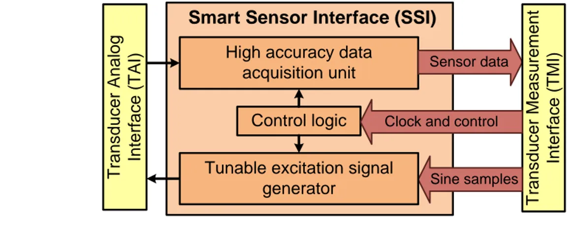
The proposed architecture of the SSI is shown in Figure 1.4 which consists of different signal paths, from sensor to network and vice versa. The sensor output feeds forward throughout an analog signal processing scheme and then is digitized using a high precision analog to digital converter and a ratio-metric unit. Afterward, the sensor data is forwarded to TIM services through Transducer Measurement Interface (TMI). The feedback path generates the excitation signal for sensors based on the amplitude and frequency information provided by the incoming data from network and adapts its level to the operating range of the sensors [1,17,16].
The Excitation Signal Generator (ESG) path links the avionics AFDX network and the position sensors. With reference to the specifications of legacy R/LVDT position sensors, it generates a sinusoidal signal with voltage levels adapted for actuating the sensors.
Considering the circuit complexity of the SSI, in this Master thesis we have focused on the design, implementation, and characterization of the ESG unit. Although there are several solutions for low-frequency sinusoidal waveform generation, a new architecture for the ESG unit should be carefully designed in order to adhere to the requirements of the proposed SSI block
High accuracy data
acquisition unit Sensor data
Smart Sensor Interface (SSI)
Control logic T ra n s d u c e r A n a lo g In te rf a c e ( T A I) T ra n s d u c e r M e a s u re m e n t In te rf a c e ( T M I) Sine samples Clock and control
Tunable excitation signal generator
Figure 1.4: Architecture of the proposed SSI
AFDX
Transducer Interface Module (TIM)
TIM services Smart Sensor Interface(SSI) Network Capable Application Processor (NCAP) Transducer Electronic Data Sheet
(TEDS) F ie ld ( C A N ) b u s
diagram. The new ESG should be programmable and can be integrated with other blocks within the SSI. Before proceeding to the literature review and design of the ESG, basic principles of displacement sensors and their interfacing requirements are described.
1.3 Basic principles of displacement sensors
The increasing applications of sensor networks and sensing devices have resulted in numerous implementation techniques. In aircrafts and avionics systems, various types of sensors and actuators are employed in order to prepare critical data for Flight Control Computers (FCC). Therefore, reliable, precise, accurate, and highly-sensitive sensors with a very long Mean-Time Between Failures (MTBF) are required to meet stringent safety standards for avionic applications. R/LVDT displacement sensors are based on Variable Differential Transformer technique and operate wear-free. They exhibit excellent linearity and resolution, possess long lifetime, and measure over a large spectrum. Hence, they perfectly comply with avionic safety standards and are widely used in flight data acquisition and servo control [2,4,11].
To clarify the terminology, position of an object is its linear or angular coordinate with respect to a selected reference. In contrast, displacement means the specific linear or circular movement of an object from one position to another. In other words, a displacement is measured by sensing the amount of motion of an object with reference to its own prior position rather than to another reference [11].
With respect to the quality and the performance of displacement sensors, they are employed to measure not only the displacement, but also some other stimuli such as force and pressure. In these cases, the stimulus should be first converted to displacement and then accurately measured by a variety of R/LVDT sensors. As an example of pressure sensing, the pressure variation could change the position of a diaphragm. Using an R/LVDT sensor, the displacement of the diaphragm can be then converted into an electrical signal representing pressure [11,18].
In order to benefit the level of performance of R/LVDTs, a highly accurate and precise sensor interface circuit is a vital requirement in the navigation of air vehicles. In this section, the physical structure and operation principles of R/LVDTs as well as the architecture of the interface circuit are briefly described.
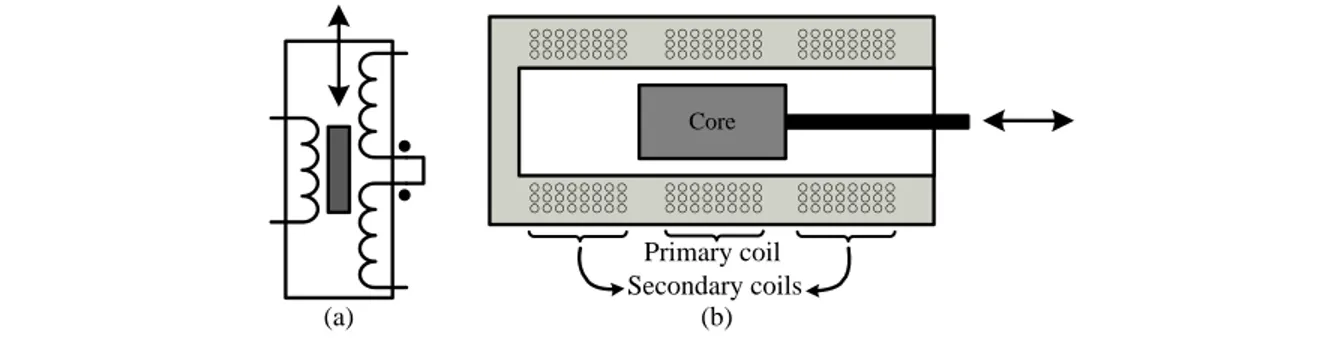
1.3.1 LVDT and RVDT inductive sensors
The Variable Differential Transformer (VDT) technique is based on the magnetic flux coupling between two or three coils which can be altered by a moving ferromagnetic core. The coils are arranged as one primary and two equally spaced, identical secondary ones. Upon exciting the primary coil with a sine waveform current and depending on the position of the core, an AC voltage is induced in the secondary coils. The core is connected to the object whose displacement is to be measured. The amount of core displacement can be extracted from the secondary signals. The sensors which use this technique are also called variable-reluctance transducers because the movable core alters the reluctance of the flux path [11].
The LVDT and RVDT electromechanical transducers use the VDT technique and are considered as magnetic or inductive type displacement sensors. When the primary coil is excited, the carrier signal is induced in the secondary coils with the same frequency contents as the excitation signal. Therefore, a pure sine wave excitation signal eliminates harmonics in the transformer and prevents errors. The movement of the ferromagnetic core within the flux path is modulated over the amplitude of the carrier signal of the secondary coils. As shown in Figure 1.5, the mechanically actuated core is coaxially inserted into a cylinder structure on which the coils are wound. The core does not physically touch the coils and thus there is no or very little friction. Being designed on the same principles as LVDT, the RVDT is capable of measuring angular displacement by using a rotary core [11,18].
In general, the two secondary coils are connected in opposite phase. So, the output of the sensor is the difference between the individual secondary voltages. Assuming fully symmetrical secondary coils, as long as the core is held in the magnetic center of the sensor, the summation of
(a) ● ● ○○○○○○○○ ○○○○○○○○ ○○○○○○○○ ○○○○○○○○ ○○○○○○○○ ○○○○○○○○ ○○○○○○○○ ○○○○○○○○ ○○○○○○○○ ○○○○○○○○ ○○○○○○○○ ○○○○○○○○ ○○○○○○○○ ○○○○○○○○ ○○○○○○○○ ○○○○○○○○ ○○○○○○○○ ○○○○○○○○ Core Primary coil Secondary coils (b)
the two output voltages remains zero. Any movement of the core toward the endings of the cylinder unbalances the secondary voltages which results in a non-zero output. In fact, the movement of the core alters the reluctance of the flux path that results in variation of the induced voltage. Hence, the amplitude and phase of the output signal represent the displacement and its direction, respectively. Obviously, the displacement information is valid in the linear operating range of the sensor [11].
The following advantages discriminate the R/LVDTs from other types of displacement sensors: (1) the penetration of any nonmagnetic material in the magnetic field generated by the primary coil, results in no loss of accuracy; (2) to be used in harsh environments and corrosive situation, R/LVDTs can be coated with inert material. Such coating does not affect the measurement; (3) as a desirable mechanical feature, there is no or very little friction or wear resistance; (4) magnetic and mechanical hysteresis is negligible; (5) in theory, the sensitivity of the sensor is infinitesimal; (6) the output impedance is very low; (7) the mechanical structure is solid and robust and they can measure over a large spectrum of displacement; (8) these transducers are static sensors. This means that their response is not a function of time [2,11,18,19].
With respect to the above-mentioned advantages, there are a variety of applications for these rugged and versatile sensors. They are employed in jet engines and hot-slab mills in order to measure force and pressure [18]. In Idaho National Engineering Laboratory (INEL), the LVDT is used to measure the elongation of the nuclear fuel rod which is an indication of critical heat flux [20]. In medical applications, authors of [21] directly placed a LVDT over the hand vein to measure the variation of its diameter (ranging from 0.8 mm to 1.4 mm) due to norepinephrine infusion. An example of a different exploitation, LVDT is used in a horticultural study in order to measure the variation of the diameter of pepper plants [22]. In addition, these transducers are widely employed in aircrafts and avionics systems including flight controls, thrust reversers, steering feedback, and landing gear [3,18,23,24,25].
1.3.2 LVDT and RVDT interfacing
Considering Figure 1.1, any interfacing circuit should be faithful to both the sensor and the data processing module. With regard to the infinitesimal sensitivity of R/LVDTs, the resolution of the
sensing system is determined by the specifications of the interfacing electronics. Thus, the design of an interface for R/LVDTs sensors is more challenging compared to other types of sensors [11]. R/LVDTs are classified as passive sensors. This means that an external source of energy is required for the operation of the sensor. Therefore, any R/LVDT interfacing circuit should include two major modules: (1) an Excitation Signal Generator (ESG); (2) a Data Acquisition Module (DAM). The ESG output should drive the sensor with a sine waveform of proper frequency and amplitude. On the other hand, the sensor output should be conditioned by front-end circuit and the DAM in order to be compatible with data processing system [11,25].
For proper excitation of primary coil, a stable sine wave generator is required in the ESG. The advantage of sinusoidal excitation signal is that proper filtering increases the achievable Signal to Noise Ratio (SNR). Nevertheless, generation of sine waveform needs more complex circuit and consumes higher power in comparison with square-wave or pulse signals. The frequency of the sine is determined by the movement speed. To accurately extract movement data, the sine frequency (the carrier frequency for amplitude modulated data) should be at least 10 times higher than the highest possible movement speed of the sensing stimulus [11]. Thus, different applications impose various sine frequencies. As a result, the adjustability of the excitation frequency is a preliminary consideration in the design of a generic SSI. According to the key features of most R/LVDT sensors and general specifications of commercially available R/LVDT signal conditioners, the sine wave output of the ESG should cover the frequency and amplitude range of 1 kHz to 20 kHz and 1 Vrms to 10 Vrms, respectively. The maximum required excitation current is 20mA [9,26,27,28,29].
In the data acquisition path of the interface, the sensor output might be too weak and noisy with undesirable interference signal components. Therefore, the analog front-end must have a very low noise figure and should be linear for the wide dynamic range of sensor output signal. High order low pass filter with a sharp cut-off knee is also needed to discriminate the data from the carrier signal. A high-resolution and high-accuracy ADC should then digitize the sensor output signals for further processing [1].
1.4 Research objectives and challenges
Keeping the SSI architecture of Figure 1.4 in mind, the following goals have been considered in this work:
- First and foremost, the frequency and amplitude of the excitation signal should be determined via the TMI. This feature guarantees the configurability of the SSI. The acceptable frequency and amplitude range for most of the Legacy R/LVDT sensors varies from 1 kHz to 10 kHz and from 1 Vrms to 7 Vrms.
- The proposed ESG should be designed based on CMOS technologies in order to make the integration of the SSI possible.
- To support one of the essential goals of the main project, the number of input/outputs between ESG and the TMI should be minimized. This feature not only decreases the required wiring connections, but also facilitates the integration of the SSI and the TMI. - In order to drive legacy R/LVDT position sensors, the final output of the ESG should
provide sufficient drive capabilities. In addition, the acceptable range of excitation signal amplitude of most legacy sensors is not fully attainable in nanometer CMOS technologies. Thus, additional circuitry should be considered in the last stage of the ESG. - To minimize the power consumption, the designed ESG must maximize the power
efficiency. Since the excitation signal is better to be of current type, this feature can be achieved by current-mode designing of main blocks.
Established goals and objectives confront with various challenges in the design, implementation and integration procedures. Any ESG architecture and specification should comply with the SSI and support the required systematic specifications. Therefore, more parameters must be taken into account in the design of ESG. Moreover, with reference to the low frequency operation of the ESG, smoothing filters may need large capacitors and/or resistors which either are not available in CMOS technologies or may impose very large or unacceptable die area.
Proper operation of data acquisition unit is tied to the accuracy and purity of the sine-wave excitation signal. Hence, the accuracy and precision of the ESG output along with the
programmability of the frequency and amplitude is yet another challenge which should be tackled in the systematic and circuit level designs.
The last challenge that faces this design is the incorporation of low voltage circuits in nanometer CMOS technologies with the required high voltage amplifier blocks as the last stages of the ESG. Achieving this goal imposes the usage of some off-chip blocks in order to drive the sensors with appropriate signal level.
1.5 Contributions
In view of the objectives that are considered and the mentioned challenges, the following contributions have been made:
- A new ESG unit has been designed which can be integrated along with a data acquisition unit in order to constitute a system-on-chip SSI module for the avionics applications. The proposed ESG architecture is fully compatible with the TIM services and configurable through the TMI block in the improved AFDX network. The whole SSI module is to be used as an important part in next generation avionics data networks which facilitate the transition of a Federated Avionic Architecture (FAA) to an Integrated Modular Avionics (IMA).
- Moreover, in chapters 3 and 4, a new parameter in the design of Segmented Current-Steering Digital to Analog Converters (SCSDAC) has been introduced. According to the simulations the performance of the switching sequence in SCSDACs depends on the physical realization of Current Source Array (CSA). To further investigate this effect, a new programmable CSA chip has been designed, laid out and submitted for fabrication. Provided that the measurement results confirm the simulation results, the choice of switching sequence should be based on the aspect ratio of the CSA. In this case, further investigation is needed to design a generic efficient sequence for specific ratios between the length and the width of the laid out CSA.
1.6 Thesis outline
The development of a programmable excitation signal generator unit within a SSI module for avionics applications shall be the subject of this work. The Master thesis is organized in four chapters and a conclusion. Following this brief introduction, the specifications of the desired smart-sensor interface as well as literature review will be presented in chapter two. Chapter three discusses the ESG design procedure in system and circuit levels. Additional details along with simulation and measurement results have been provided in chapter four. The conclusions and outcome drawn from this research are explained in the final chapter which also includes some future directions for circuit designs and system-level integration.
CHAPTER 2
BACKGROUND ON EXCITATION SIGNAL GENERATION AND R/LVDT
INTERFACING
2.1 Introduction
The purpose of this chapter is to review the published articles and commercial interfacing solutions and excitation signal generation methods for R/LVDT displacement sensors. This brief survey as well as fundamentals of R/LVDTs presented in chapter one, help the readers to better understand the topic of this Master thesis.
In the first step, the benefits and challenges of smart and integrated sensing systems will be discussed. To cover our application, we have then focused on commercially available solutions which can drive legacy displacement sensors and demodulate their outputs. Several papers with the same topic will also be presented. Afterwards, the published methods of excitation signal and sine waveform generation will be discussed. Finally, with reference to our selected architecture for realization of the ESG, the design of the Current-Steering Digital to Analog Converters (CSDAC) will be reviewed.
2.2 Integrated sensing systems
Since the late 1970s when the Fly-By-Wire (FBW) flight control systems came into use, the aerospace industry has evolved toward designing More Electric Aircrafts (MEA) instead of relying on conventional hydraulic, mechanical, and air/pneumatic avionics systems. The MEA approach has improved the efficiency, reliability, and maintainability of avionics systems. It has also resulted in lighter aircrafts which can lead to reduced fuel consumption in a highly competitive market [30,31].
In support of this trend, Integrated Sensing Systems (ISS) has been developed in order to miniaturize, reduce the cost, size, power consumption, and weight of the sensor systems. Sensing,
signal conditioning, analog to digital conversion, bus interfacing, and data processing are main functions of any ISS. Hence, the ISS may include the sensor, amplifier, Analog to Digital Converter (ADC), buffer, and bus interface. To further improve the quality of the system, built-in self-testing, auto-calibration, and data evaluation modules can be integrated in ISS. Depending on the integration compatibility of the sensor and the allowance of the technology, different levels of integration are expected which are shown in Figure 2.1 [9]. On the other hand, a set of smart transducer interface standards named IEEE-1451, have been developed to standardize different solutions for connecting sensors and actuators to instrumentation systems [12,13].
ISS is associated with numerous benefits and challenges. Sharing of multifunction modules, common module production, canceling the effects of cable and wire impedances, and employing mature technologies in robust and reliable designs are major strong points of this design methodology. Moreover, ISS facilitates the succession of integrated modular avionics and reduces the amount of equipment installed on the aircraft. At the same time, it increases the efficiency of communication between coupled functions. However, there are some challenges in the top-down and bottom-up ISS design approaches. The high cost of integration will be reasonable only in case of mass production. In other words, the size of the market determines the level of integration of sensing systems. Another negative aspect is that the integration must be consistent with the required level of redundancy in order to maintain the desired reliability. Also,
Sensor Analog Digital Bus Data Bus Encapsulation Universal sensor interface Sensor Analog Digital Bus Sensor Analog Digital Bus Sensor Analog Digital Bus Improved hybrid solution Local-bus one chip solution Future one chip solution
the parasitic electrical effects on the sensing elements should be carefully taken into account [9,32,33,34].
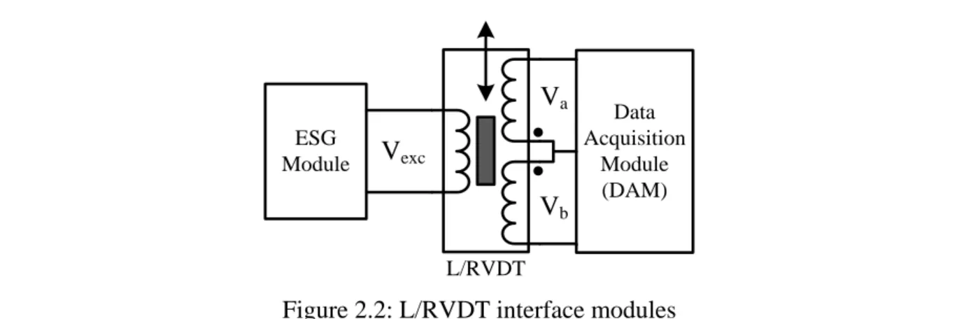
2.3 L/RVDT integrated interfacing
Using discrete electronic components and designing Application Specific Integrated Circuit (ASIC) are two traditional solutions to interface L/RVDT sensors [35]. With respect to Figure 2.2, the system and circuit level designs of the ESG and the DAM should be consistent and uniform in any integrated interface solution (will be referred as SSI in this Master thesis) for L/RVDT sensors. Besides, the specifications of each module should be determined with regard to those of the other module. In other word, the required performance of each module depends on the desired characteristics of the whole interface as well as the specifications of the other module. As an example, generation of a highly-precise, high-SNDR sine waveform in the ESG decreases the order of filter in the DAM.
In a fully integrated SSI, the integrability of the ESG and the DAM is the most important requirement. Another obligation is that the frequency and amplitude of the excitation signal must be set by the TMI which is part of the TIM introduced in IEEE-1451 [16]. Since the TMI is a digital block, the proposed design of the ESG should be able to receive the sine waveform parameters through a digital signal. Considering the commercial displacement sensors and respecting the AVIO402 demands, the ESG must generate a sine waveform in the frequency range of 1 kHz and 10 kHz with an accuracy of 1%. Since the information bandwidth is rather small in L/RVDTs, multiple measurements can be performed in the desired frequency range.
● ● ESG Module Data Acquisition Module (DAM) L/RVDT Vexc Va Vb
Thus, 30 different excitation frequency channels have to be covered by ESG. In the DAM, sensor output signals should be conditioned, filtered and averaged for further analog or digital signal processing. Moreover, each sensor channel should be filtered from the other channels to avoid cross talk between neighbor sensing systems [1,26,28,29].
Interfaces designed by fully analog electronics, suffer poor long-term performance, comprise many components, and are hard to adjust. They also lack the communication with computers and microcontrollers. Programmable digital and mixed-signal circuits are used in newer interfaces. Drumea et al. [36] have used MSP430F149 microcontroller (MCU) produced by Texas Instruments, to bring together data conversion blocks, timer, digital memory, and PWM module. On-chip 12-bits ADC, comparator, timer, Universal Synchronous-Asynchronous Receiver-Transmitter (USART), as well as ultralow-power consumption, and built-in memory make it a powerful target for this application. One of the timers can generate a pulse-width modulated (PWM) signal which is filtered to produce a sine waveform. This stable 5 kHz sine signal is then buffered by two external operational amplifiers to source the required excitation current to the primary coil of the sensor. A discrete differential amplifier is then used to apply the sensor output signals to the ADC of the MCU. Using external DAC and/or RS232 interface, the displacement value can be sent to other systems. This interface electronics has been fabricated on a two layer PCB with 50 x 40 x 20 mm dimensions. Although the interface precision is reported to be ±0.3% with a calibrated algorithm, it has been only connected to a special LVDT built by Research Institute for Hydraulics and Pneumatics. A fixed sine frequency and no measured data on the quality of the sine is another weak point of this report. On the other hand, this MCU cannot be integrated with the TMI and the TIM services which further limit our design strategy.
STM32F103RC MCU from STMicroelectronics is used by Wang et al. in [35] in order to design an intelligent acquisition module for differential transformer position sensors. In this architecture, a sine-wave memory inside the MCU sequentially sends the sine samples to the on-chip 12-bits DAC. Two off-chip operational amplifiers filter and buffer DAC output and excite the sensor. Sensor output signals are then amplified or attenuated (depending on the signal level) and applied to the MCU through a matching circuit. In addition to the sine-wave generator and signal acquisition units, the MCU realizes signal processing, calculation, calibration, and communication modules. Although [35] is a complete L/RVDT interface and the authors have claimed that it generates pure sine-wave, no measurement result has been reported. Besides, it has
the same drawback as [36] in integrating MCU in the NCAP in order to centralize interface control module. Nevertheless, the idea of using a digital sine-sample memory has been used in our design which will be discussed in chapter 3.
In another similar approach, PCI1716 card from Advantech is configured as a powerful data acquisition module for L/RVDT sensors in [37]. It can receive 16 single ended or 8 differential channels. The complete data acquisition system contains the PCI1716, the PCLD-8710 wiring terminal board, and an Industrial PC (IPC). The PCI card includes 16-bits ADC, 1024 samples FIFO, 32 digital inputs and outputs, and 2 analog output channels with 20mA driving capability. 0.01 mm is the best achieved precision in this user-friendly and software programmable interface, however, it is not a proper solution for avionics application due to the cost, non-integrability, size, and required wiring connections.
Canu et al. [38] have presented a versatile input interference for avionic computers. Their general interface solution fills the requirements of four types of most common input and outputs of avionic computers: (1) discrete Input Vdd/Open; (2) Discrete Ground/Open; (3) L/RVDT acquisition; (4) ARINC429 receiver. Drastically decreasing the complexity of I/O boards, it results in more flexible interface boards that occupy less physical area in avionic computers. Unfortunately, this generic solution only interfaces L/RVDTs to the computer and cannot generate the excitation signal or perform any data processing scheme.
There are few commercially available signal conditioner subsystems for L/RVDTs. Analog Devices single chip solutions, AD598 and AD698, convert sensor signals to an accurate unipolar or bipolar DC voltage proportional to the physical displacement. Both chips need a few external passive components to set the signal conversion gain and excitation signal (Vexc) frequency and amplitude [39,40]. They can drive the sensor primary coil with an excitation sine in the frequency range of 20 Hz to 20 kHz and up to 24Vrms. Total harmonic distortion of the sine is claimed to be -50 dB. Being set by external resistors and capacitors, the amplitude and frequency of the excitation signal as well as the gain of the chip will be fixed and cannot be programmed. Moreover, any inaccuracy or temperature drifts of passive components cause amplitude and frequency distortion in Vexc and output voltage. The outputs of AD598 and AD698 are calculated based on Eqs. (2.1) and (2.2), respectively.
(2.1)
(2.2)
where is the excitation voltage and and are secondary voltages of the L/RVDT, as shown in Figure 2.2.
In Eq. (2.1), it is assumed that is a fixed value which should be measured and used as a parameter in the design procedure. However, this term is proportional to the . Thus, any variation of excitation voltage will cause nonlinearity in the displacement measurement. In the AD698, the direction of the displacement cannot be detected because of using the absolute difference value between sensor outputs in the numerator of Eq. (2.2). Consequently, AD598 and AD698 cannot be employed in our application due to their integrability and non-programmability.
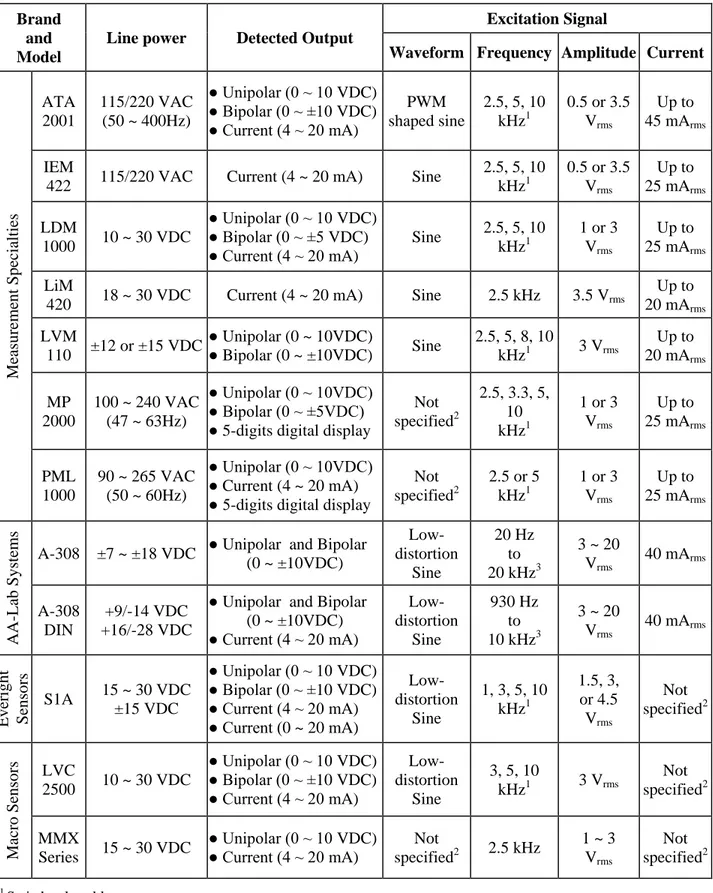
Several manufacturers produce different models of L/RVDT signal conditioner units which perform excitation, amplification, demodulation, signal modification, and readout [27,41,42,43]. Table 2.1 summarizes the specifications of these models. They can be employed in many industrial instrumentation applications to excite various L/RVDTs and detect their output signals. However, there are many incompatibilities in using them within avionics systems. They are not compatible with IEEE-1451 since they cannot be configured by a centralized control block. The excitation signal frequencies are also limited and cannot be digitally controlled. Additionally, the outputs are in the form of analog voltage and/or current signals. No analog to digital convertor has been provided in these products. Non-integrability and large physical dimensions are other factors which makes them improper for our application. Nonetheless, the presented specifications clarifies and justifies our selected objectives and design parameters stated in chapter one.
In summary, any solution for avionic sensing system and its building blocks should be integrable and programmable in order to be used in IMA systems. With respect to the development of sensor network architectures in MEAs, it must also be versatile and compatible with a centralized control system and/or network gateways. In the rest of this chapter, we will focus on the different methods used in design and realization of a sine waveform generator as the core of the ESG.
Table 2.1: Specifications of commercial L/RVDT signal conditioners
Brand and Model
Line power Detected Output
Excitation Signal
Waveform Frequency Amplitude Current
Measure me nt Sp ecia lties ATA 2001 115/220 VAC (50 ~ 400Hz) ● Unipolar (0 ~ 10 VDC) ● Bipolar (0 ~ ±10 VDC) ● Current (4 ~ 20 mA) PWM shaped sine 2.5, 5, 10 kHz1 0.5 or 3.5 Vrms Up to 45 mArms IEM
422 115/220 VAC Current (4 ~ 20 mA) Sine
2.5, 5, 10 kHz1 0.5 or 3.5 Vrms Up to 25 mArms LDM 1000 10 ~ 30 VDC ● Unipolar (0 ~ 10 VDC) ● Bipolar (0 ~ ±5 VDC)
● Current (4 ~ 20 mA) Sine
2.5, 5, 10 kHz1 1 or 3 Vrms Up to 25 mArms LiM
420 18 ~ 30 VDC Current (4 ~ 20 mA) Sine 2.5 kHz 3.5 Vrms
Up to 20 mArms LVM 110 ±12 or ±15 VDC ● Unipolar (0 ~ 10VDC) ● Bipolar (0 ~ ±10VDC) Sine 2.5, 5, 8, 10 kHz1 3 Vrms Up to 20 mArms MP 2000 100 ~ 240 VAC (47 ~ 63Hz) ● Unipolar (0 ~ 10VDC) ● Bipolar (0 ~ ±5VDC) ● 5-digits digital display
Not specified2 2.5, 3.3, 5, 10 kHz1 1 or 3 Vrms Up to 25 mArms PML 1000 90 ~ 265 VAC (50 ~ 60Hz) ● Unipolar (0 ~ 10VDC) ● Current (4 ~ 20 mA) ● 5-digits digital display
Not specified2 2.5 or 5 kHz1 1 or 3 Vrms Up to 25 mArms AA -Lab Sy st em s
A-308 ±7 ~ ±18 VDC ● Unipolar and Bipolar (0 ~ ±10VDC) Low-distortion Sine 20 Hz to 20 kHz3 3 ~ 20 Vrms 40 mArms A-308 DIN +9/-14 VDC +16/-28 VDC
● Unipolar and Bipolar (0 ~ ±10VDC) ● Current (4 ~ 20 mA) Low-distortion Sine 930 Hz to 10 kHz3 3 ~ 20 Vrms 40 mArms Ev erigh t Senso rs S1A 15 ~ 30 VDC ±15 VDC ● Unipolar (0 ~ 10 VDC) ● Bipolar (0 ~ ±10 VDC) ● Current (4 ~ 20 mA) ● Current (0 ~ 20 mA) Low-distortion Sine 1, 3, 5, 10 kHz1 1.5, 3, or 4.5 Vrms Not specified2 Macro Senso rs LVC 2500 10 ~ 30 VDC ● Unipolar (0 ~ 10 VDC) ● Bipolar (0 ~ ±10 VDC) ● Current (4 ~ 20 mA) Low-distortion Sine 3, 5, 10 kHz1 3 Vrms Not specified2 MMX Series 15 ~ 30 VDC ● Unipolar (0 ~ 10 VDC) ● Current (4 ~ 20 mA) Not specified2 2.5 kHz 1 ~ 3 Vrms Not specified2 1 Switch selectable 2
In the online datasheet
3
2.4 Sine wave generation methods
Considering the overall performance of the SSI, sinusoidal signal is the most efficient waveform to excite an L/RVDT sensor. Contrary to square, periodic exponential and quasi-sine waveforms, a pure sine wave has only one dominant frequency component. Exciting the L/RVDT with a sine-waveform induces the same frequency component in the signal spectrum of the sensor outputs. This characteristic decreases the order of the low pass filter in both ESG and DAM. The desired 14-bits resolution in the DAM of our SSI necessitates the design of a high-accuracy sine-wave generator in the ESG. The generator block should cover 1 kHz to 10 kHz frequency range.
According to the research papers and commercial products, sine-wave generators are based on three different techniques, namely: (1) Analog oscillator; (2) Non-linear circuits; (3) DSP1 and memory-based. The choice of the architecture depends on the desired signal quality. In oscillators, a tunable component sets the frequency. Covering a limited frequency-tuning range, they are highly affected by temperature variation and component tolerances. Non-linear circuits usually transform a triangular wave to a sine by utilizing a nonlinear-transfer function. They cover a wider frequency range but are perturbed by temperature changes. In integrated realizations, the process variations of semiconductor devices and mismatches further decrease the accuracy and precision of the oscillators and non-linear solutions [44]. Both techniques are not programmable and thus, cannot be involved in our application.
DSP and memory-based architectures are mixed-signal circuits which employ DSP, digital memory, microcontroller, or digital logic circuitry along with a DAC to generate an arbitrary waveform. As depicted in Figure 2.3, the samples of the expected waveforms are stored in a digital or analog memory. Depending on the shape of the signal, an addressing algorithm reads out one stored sample in each clock cycle and applies it to the DAC for conversion to an analog equivalent. The clock rate and the number of retrieved samples in each cycle determine the frequency of the output signal. A filter, amplifier, and/or matching circuit follow the DAC to improve the quality of the signal. A DSP or MCU can be used to implement the clock module, the memory address controller, and the digital memory. This method is widely used in Arbitrary
1
Function Generators (AFG) and Arbitrary Waveform Generators (AWG) [45,46]. The large required physical size of the memory and other digital blocks is the drawback of this technique.
In 2009, Yang et al. have designed a hybrid architecture to generate quadrature sine waveforms in seven orders of frequency range from 1 mHz up to 10 kHz [44]. To cover the range of 100 Hz to 10 kHz which overlaps our application, they have used a resistor-chain DAC (RCDAC). It includes a resistor-chain followed by a track-and-hold circuit and a gm-C biquadratic low pass filter with selectable cutoff frequencies. The resistor-chain is a voltage divider with 33 different taps which are representing analog samples of a half-cycle sine waveform. Therefore, the chain could create a set of 64 samples of a complete cycle of a sine. An overall SFDR2 of -50dB is expected from the 64x OSR3. A clock divider divides the 10 MHz master clock ( ) frequency by an integer number, M, to control the DAC switches. Synchronously with the clock and consecutively, tap voltages are conducted to the DAC output in order to form the sine wave. The output frequency ( ) can be calculated using Eq. (2.3).
(2.3)
The authors of [44] used the RCDAC as an analog memory to avoid the large physical area needed for a digital memory. The matching between resistors and the on resistance of the switches are the most important factors affecting the linearity and performance of this architecture. To achieve a high linearity, 1000 same-size resistors were utilized in the chain to form unequal resistances between taps. Simple NMOS transistors are used as switches which simplify the control logic. Occupied 1 mm2, the design is fabricated in 0.5µm CMOS process. Contrary to the design objective (-50dB) a THD of less than -44dB (0.6 %) across the entire frequency range has been reported.
2
Spurious Free Dynamic Range
3
Over Sampling Ratio Clock module Memory address control Waveform memory Analog output circuit DAC Output signal External clock
![Figure 2.7: Current steering DAC (a) Thermometer code, (b) Binary-weighted code [47]](https://thumb-eu.123doks.com/thumbv2/123doknet/2334012.32369/42.918.111.815.429.680/figure-current-steering-dac-thermometer-code-binary-weighted.webp)
![Figure 2.8: Segmented current steering DAC [49]](https://thumb-eu.123doks.com/thumbv2/123doknet/2334012.32369/43.918.116.703.184.400/figure-segmented-current-steering-dac.webp)