UNIVERSITÉ DE MONTRÉAL
INTEGRATED GUIDED-WAVE STRUCTURES AND TECHNIQUES FOR MILLIMETER-WAVE AND TERAHERTZ ELECTRONICS AND PHOTONICS
FAEZEH FESHARAKI
DÉPARTEMENT DE GÉNIE ÉLECTRIQUE ÉCOLE POLYTECHNIQUE DE MONTRÉAL
THÈSE PRÉSENTÈE EN VUE DE L’OBTENTION DU DIPLÔME DE PHILOSOPIAE DOCTOR
(GÉNIE ÉLECTRIQUE) AOÛT 2016
UNIVERSITÉ DE MONTRÉAL
ÉCOLE POLYTECHNIQUE DE MONTRÉAL
Cette thèse intitulée :
INTEGRATED GUIDED-WAVE STRUCTURES AND TECHNIQUES FOR MILLIMETER-WAVE AND TERAHERTZ ELECTRONICS AND PHOTONICS
présentèe par : FESHARAKI Faezeh
en vue de l’obtention du diplôme de : Philosophiae Doctor a été dûment acceptée par le jury d’examen constitué de :
M. KASHYAP Raman, Ph. D., président
M. WU Ke, Ph.D., membre et directeur de recherche
M. CHAKER Mohamed, Ph. D., membre et codirecteur de recherche M. CARDINAL Christian, Ph. D., membre
DEDICATION
Dedicated with love and gratitude to:
ACKNOWLEDGEMENTS
My deepest gratitude is to my thesis supervisor, Prof. Ke Wu, for his inspirational mentorship, constant encouragement, and constructive criticisms. Prof. Ke Wu offered his unreserved help and guidance throughout my graduate studies. He guided me through tough times and was always with me to check on my research progress. I am deeply grateful to him for the long discussions we had, for holding me to a high research standard and enforcing strict validations for each research result, and therefore teaching me how to do research.
I am deeply grateful to Prof. Mohamed Chaker, my co-supervisor, director of Laboratory of micro- and nanofabrication (LMN). He was always eager to help me and I am grateful to him, for being friendly, caring, supportive and helpful in numerous ways. I am indebted to him for his continuous encouragement and guidance.
I also thank Dr. Tarek Djerafi and Dr. Nadir Hossain with whom I had very educative interactions during my research. I am also very grateful to all the personnel at the Poly-Grames Research Center, especially all the technicians including Mr. Jules Gauthier, Mr. Traian Antonescu, Mr. Steve Dubé and Mr. Maxime Thibault. My gratitude extends to Mrs Rachel Lortie for her assistance with all the administrative works and also to Mr. Jean-Sébastien Décarie for his technical support for solving all the IT problems. I am also very grateful to all the personnel at LMN, especially Dr. Sébastien Delprat, Dr. Boris Le Drogoff and also Ms. Johanne Roy. I would like to thank all my friends and colleagues in the Poly-Grames Research Center and LMN.
I would also like to thank my family for the support they provided me through my entire life and in particular, I would like to express my heartfelt gratitude to my husband, Hadi Razavipour, without whose love and encouragement, I would not have finished this thesis.
RÉSUMÉ
Pour faire face à la demande croissante en bande passante, les prochaines générations des systèmes sans fil et filaires devront exploiter la large gamme spectrale 100 GHz-1 Térahertz (THz) et au-delà. Cependant, les éléments constitutifs intégrés qui définiront les architectures et les normes des systèmes à très haute fréquence ne sont pas claires et généralement pas du tout disponible. Cette thèse contribue à ce nouveau défi en explorant de nouveaux concepts et techniques de transmission d’onde pour le développement des circuits intégrés et les systèmes électroniques et photoniques en ondes millimétriques (MMW) et THz.
Les lignes de transmission sont les éléments constitutifs de tous les circuits électroniques et photoniques intégrés. En dépit d'une expansion substantielle des applications électroniques et photoniques vers les THz, la structure de base des lignes de transmission standard, mis au point dans les années 1950, n'a pas évolué. L'un des problèmes fondamentaux dans le développement de systèmes électroniques et photoniques intégré THz est les limites intrinsèques de ces lignes de transmission classiques. Les dispositifs à ondes progressives électro-optiques et optoélectroniques ont été conçus sur la base de ces lignes de transmission, et sont donc limités en débit en raison de la limitation des performances au spectre RF. Plusieurs tentatives ont été faites pour améliorer ces lignes de transmission. Cependant, la configuration structurelle inhérente du métal est toujours l'obstacle dominant qui impose un mode de fonctionnement particulier qui est sujette à l'atténuation et la dispersion à une fréquence plus élevée. Pour faire face aux problèmes mentionnés et pour répondre à ces défis technologiques contraignants, trois orientations sont traités dans cette thèse: électro-optique, micro-ondes et optique.
Pour la première orientation, la ligne SIW est utilisée en tant que structure à onde progressive alternative d'un Modulateur EO sur polymère. Dans ce cas, la fréquence porteuse est déterminée par la fréquence de fonctionnement de la ligne SIW. Dans ce travail, la conception est faite pour un modulateur EO atteignant plus de 22% de la bande passante optique avec la fréquence centrale de 160 GHz.
En ce qui concerne la deuxième orientation, une ligne de transmission entièrement intégré avec une topologie simple est réalisée pour surmonter les problèmes persistants de forte atténuation, forte dispersion et faible confinement de mode dans la transmission du signal guidé du DC au THz. En conséquence, le concept et la conception d'une ligne de transmission "intelligente" à faible perte
et à faible dispersion de propagation du signal sur toute gamme de fréquences DC - Térahertz (THz) sont introduites, et démontrés. La ligne que l'on appelle la ligne de transmission a mode sélectif ou simplement "MSTL" fonctionne avec un comportement de commutation de mode dépendamment de la fréquence; la conception est réalisée de telle sorte qu’avec la croissance de la fréquence, un phénomène de "conversion" mode a lieu et le mode de fonctionnement est automatiquement reconfiguré intentionnellement et sans aucune intervention extérieure afin d'assurer une faible perte et une faible dispersion. Une approche théorique combinée avec des simulations avec un logiciel (3D) à ondes complètes et des mesures expérimentales est utilisée pour vérifier le concept et la structure proposée. Comme l'une des applications fondamentales, des interconnexions, y compris via une ligne et un coude, sont étudiées et conçues. MSTL est fabriqué en deux plates-formes de substrat différentes (quartz et du PCB) et caractérisé de DC à 500 GHz. La caractérisation est effectuée dans les domaines spectral et temporel pour examiner et vérifier la propagation des impulsions d'une durée de picosecondes, des impulsions rectangulaires numériques à haute débit et aussi pour obtenir et analysé un diagramme de l'œil. La diaphonie des lignes placé côte à côté est également mesurée pour confirmer les performances pour les interconnexions à haute densité. Cette technologie a permis, pour la première fois, la transmission d'impulsions avec débit ultra-rapide le long des lignes de transmission avec une dispersion et des pertes beaucoup plus faible que les technologies actuelles. Une méthode uniformisée destinée à extraire le modèle circuit et à calculé l'impédance caractéristique d’une ligne de transmission ou d’un guide d'onde avec profile ou mode arbitraire a également été mise en place, cette technique peut être appliquée pour obtenir l’impédance caractéristique de la ligne MSTL sur toute la bande de fréquence d'intérêt.
Dans la dernière orientation, un guide d'onde optique à faible perte et un coupleur optique à réseau de diffraction à haute efficacité ont été conçus et optimisés. Le guide d'onde optique est conçu sur la base de baryum et de calcium niobate (CBN), qui est un nouveau matériau électro-optique à haute performance et qui est disponible en film mince ainsi que en vrac. Une analyse Trois dimensionnels (3D) a onde complète d'un coupleur à réseau de diffraction hors-plan est réalisé pour la première fois et le diagramme de rayonnement ainsi que les caractéristiques sont dérivées. La conception et l'optimisation des deux structures ont été validées par la fabrication et la caractérisation.
Enfin, le dernier chapitre présente les conclusions de la thèse et propose les potentiel futurs travaux dans le domaine de mmW / THz électronique et photonique
ABSTRACT
In order to keep up with rising global demand for bandwidth, future generations of both wireless and wireline technology will need to exploit the spectral range over 100 GHz - 1 terahertz (THz) and beyond. However, the integrated building blocks that will well define such an ultra-high frequency system technology architecture and protocol are unclear and mostly unavailable. This dissertation set the stage in responding to this emerging challenge by exploring new guided wave structures, concepts and techniques for the development of millimeter-wave (mmW) and THz electronic and photonic integrated circuits and systems.
Radiofrequency integrated circuits are the backbone of all modern computing and communication electronic and photonic networks and systems. Likewise, transmission lines are the most fundamental building blocks of all the electronic and photonics integrated circuits. In spite of a substantial expansion of electronic and photonic applications towards THz, the basic structure of traditional transmission lines, developed in the 1950s, has not been modified or evolved. One of the fundamental bottlenecks in the development of THz integrated electronic and photonic systems has been the inherent limitations of those conventional transmission lines. The traveling-wave electro-optic and opto-electronic devices have been made based on those transmission lines, and are therefore limited in speed because of the RF spectrum performance limitations. Several attempts have been made to improve those transmission lines. However, the inherent structural configuration is still the dominant obstacle that dictates a particular operating mode that is prone to attenuation and dispersion at higher frequencies. To tackle those mentioned problems and to respond to those constraining technological challenges, three research orientations are considered in this PhD thesis: electro-optic, microwave, and optics.
For the first orientation, SIW (substrate integrated waveguide) is used as an alternative traveling-wave structure of a polymer EO modulator. In this case, the carrier frequency is determined by the SIW frequency of operation. The design in this work is completed for an EO modulator with the center frequency of 160 GHz achieving more than 22% optical bandwidth.
With respect to the second orientation, a fully integrated transmission line with simple topology is realized to overcome the long-standing bottleneck problems of high attenuation, high dispersion, and low mode confinement in the guided signal transmission from DC to THz. Accordingly, the concept and design of a “smart” transmission line for low-loss and low-dispersion signal
propagation over the entire DC-to-THz frequency range is introduced and demonstrated. The so-called mode-selective transmission line or simply “MSTL” operates with frequency-dependent mode-switching behavior; the conception is accomplished in such a way that with increasing frequency, a “mode-conversion” phenomenon takes place and the operating mode is reconfigured intentionally and automatically without any external intervention to ensure a desired low-loss and low-dispersion performance. A theoretical approach together with full-wave three-dimensional simulations and experimental measurements is developed to verify the concept and the proposed structure. As one of the fundamental applications, MSTL interconnects, including lines and bends, are studied and designed. MSTL is fabricated in two different platforms of quartz substrate and PCB and characterized from DC to 500 GHz. The characterization is carried out in both frequency domain and time domain to examine and verify the propagation behaviors of picosecond pulses, high frequency digital rectangular pulses, and to obtain the eye-diagram. The crosstalk of the side-by-side placed lines is also measured to confirm the performance for high-density interconnects. This technology allows, for the first time, the transmission of fast pulses along the transmission lines with much lower dispersion and loss than the today’s technologies. A unified method for extracting the circuit model and calculating the characteristic impedance of arbitrary transmission line and waveguide in connection with any type of mode is also introduced, and may be applied to obtain the MSTL characteristic impedance over all frequencies of interest.
In the last orientation, low-loss optical waveguide and high-efficiency optical grating coupler have been designed and optimized. The optical waveguide is designed based on calcium barium niobate (CBN), which is a high performance novel electro-optic material and is available in thin-film as well as bulk form. Three-dimensional (3D) full-wave analysis of an out-of-plane grating coupler is achieved for the first time, and the radiation pattern and characteristics are derived. The design and optimizations of both structures have been validated through fabrication and characterization. Finally, the last chapter provides the conclusions of the thesis and outlines some of the future works planned in the field of mmW/THz electronics and photonics.
TABLE OF CONTENTS
DEDICATION ... III ACKNOWLEDGEMENTS ... IV RÉSUMÉ ... V ABSTRACT ... VII TABLE OF CONTENTS ... IX LIST OF TABLES ... XIV LIST OF FIGURES ... XV LIST OF SYMBOLS AND ABBREVIATIONS ... XXIIICHAPTER 1 INTRODUCTION ... 1 Overview ... 1 Motivation ... 3 Millimeter-wave photonics ... 5 Terahertz electronic ... 6 Objective ... 7
Methodology and contributions ... 7
Non-TEM mode electro-optical modulator for mmW and THz applications ... 7
Devising and demonstrating low-loss and low-dispersion transmission lines ... 9
Design and demonstration of the optical waveguide and modulator based on CBN . 11 Thesis roadmap ... 13
CHAPTER 2 ARTICLE 1 : BAND-PASS NON-TEM MODE TRAVELING-WAVE ELECTRO-OPTICAL POLYMER MODULATOR FOR MILLIMETER-WAVE AND TERAHERTZ APPLICATION ... 15
Introduction ... 16
Polymer electro-optic material and modulator ... 18
Substrate integrated waveguide ... 19
Contribution of this work ... 20
Device structure ... 21
Theory ... 24
Millimeter-wave driving power ... 24
Modulation frequency response ... 26
Results and parametric discussion ... 29
Optimization ... 33
Conclusion ... 38
Appendix ... 39
References ... 40
CHAPTER 3 ARTICLE 2 : LOW-LOSS AND LOW-DISPERSION TRANSMISSION LINE OVER DC-TO-THZ SPECTRUM ... 46
Introduction ... 47
MSTL concept and design parameters ... 50
Fabrication and measurement ... 56
Fabrication ... 58
Device measurements ... 58
Time domain characterization ... 59
Results ... 59
Conclusion ... 61
References ... 61
CHAPTER 4 ARTICLE 3 : GUIDED-WAVE PROPERTIES OF MODE-SELECTIVE TRANSMISSION LINE ... 66
Introduction ... 68
General ... 68
Theoretical background ... 69
Contribution of this work ... 71
MSTL structure and operation principle ... 71
Theoretical description ... 73
Background ... 73
Mode coupling and mode conversion in MSTL ... 73
Discussion ... 75
Design considerations and MSTL simulation ... 76
MSTL waveguiding characterization ... 80 Modal analysis ... 80 Loss Derivation ... 81 Parametric Study ... 83 Experimental verifications ... 89 Fabrication ... 89 Measurements ... 90 Conclusions ... 94 References ... 95
CHAPTER 5 ARTICLE 4 : MODE-SELECTIVE TRANSMISSION LINE FOR TERABIT-PER-SECOND ON-CHIP INTERCONNECTS ... 100
Introduction ... 102
Design and optimization ... 105
Fabrication and measurement ... 108
Attenuation ... 110
Dispersion ... 113
Signal reflection and ringing ... 114
Signal delay and distortion ... 115
Crosstalk ... 116
Conclusion ... 117
References ... 118
CHAPTER 6 ARTICLE 5 : S-PARAMETER DE-EMBEDDING ALGORITHM AND ITS APPLICATION TO SUBSTRATE INTEGRATED WAVEGUIDE LUMPED CIRCUIT MODEL EXTRACTION 122 Introduction ... 123
Circuit modeling ... 123
Numerical calibration ... 124
Contribution of this work ... 126
Description of method ... 127
Derivation of equations ... 129
Characteristic impedance calculation from de-embedded s-parameters ... 135
Results ... 137
Method validation ... 139
Application example: SIW ... 140
Conclusion ... 145
Appendix A ... 147
Appendix B ... 149
CHAPTER 7 ARTICLE 6 : THEORETICAL ANALYSIS AND EXPERIMENTAL
EVALUATION OF SIO2-CBN-MGO RIB WAVEGUIDE STRUCTURE ... 154
Introduction ... 155
Design and simulation ... 157
Fabrication ... 160
Characterization and experimental evaluation ... 161
Conclusions ... 163
References ... 164
CHAPTER 8 ARTICLE 7 : ACCURATE THEORETICAL AND EXPERIMENTAL CHARACTERIZATION OF OPTICAL GRATING COUPLER ... 166
Introduction ... 167
Method of Analysis ... 169
Simulations and Calculations ... 172
Fabrication and Measurement ... 179
Conclusion ... 180
References ... 181
CHAPTER 9 GENERAL DISCUSSION ... 183
CHAPTER 10 CONCLUSIONS AND FUTURE WORK ... 186
Conclusions ... 186
Future work ... 187
LIST OF TABLES
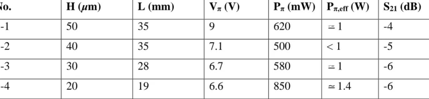
Table 2.1: Calculated driving power, driving voltage, and attenuation for 160 GHz SIW modulator
with different height and length, r=30 pm/v ... 35
Table 2.2: Calculated driving power, driving voltage, and attenuation for 160 GHz SIW modulator with different height and length, r=90 pm/v ... 35
Table 2.3: Calculated bandwidth, maximum modulation efficiency, and FOM for different designs of 160 GHz SIW modulator ... 38
Table 2.4: Calculated bandwidth, maximum modulation efficiency, and FOM for different designs of 160 GHz SIW modulator ... 38
Table 4.1: Electric and Magnetic Field Distribution in the proposed MSTL on Fused Silica Substrate at Different Frequencies: Propagating Modes Change from TEM to TE10 Mode . 81 Table 4.2: Electric and Magnetic Field Distribution in the Proposed MSTL made on Rogers Substrate for Different Frequency points: Propagating Modes Change from TEM Mode to TE10 Mode ... 88
Table 5.1: Electric and Magnetic Field Distribution in the Proposed MSTL made on Rogers Substrate at Different Frequency points: Propagating Mode Changes from TEM Mode to TE10 Mode ... 107
Table 5.2: TL attenuation summary ... 111
Table 5.3: Rectangular Pulse (50 ps width, 1ps rise time) Propagation through Microstrip line and MSTL ... 113
Table 6.1: Comparison among numerical de-embedding techniques ... 125
Table 6.2: Comparison between wave ports and lumped ports ... 128
LIST OF FIGURES
Figure 1.1: Schematic representation of electronic revolution and its driving technologies. ... 2 Figure 1.2: History of transmission line: with increasing edge speeds, wires have been replaced
with TEM transmission lines. ... 3 Figure 1.3: Terahertz electronics and millimeter-wave photonics overlap and contribution of this
thesis. ... 12 Figure 2.1: Schematic representation of polymeric substrate integrated waveguide (SIW)
modulator. ... 22 Figure 2.2: Cross-sectional view of the first proposed device showing the push-pull operation in a
polymer EO MZM. Black and gray arrows represent poling and modulation field directions, respectively. ... 22 Figure 2.3: Cross-sectional view of the second proposed device showing the push-pull operation
in a polymer EO MZM. Black and gray arrows represent poling and modulation field directions, respectively. ... 22 Figure 2.4: a) SIW structure b) TE10 Electric field propagation along the waveguide c) TE10 Electric
field distribution in the waveguide cross section. ... 23 Figure 2.5: Calculated attenuation as a function of frequency for polymer SIW modulator and
polymer MSL modulator. SIW width weff=20 μm, MSL width m, Height is changing 10 μm
to 50 μm. The adopted approach for calculations has already been examined and validated for thick film SIW [44] and for MSL in [42]. ... 30 Figure 2.6: Calculated millimeter-wave effective index as a function of frequency for polymer SIW
modulator and polymer MSL modulator compared to the optical refractive index. SIW width “w” changes from 800 μm to 1000 μm. ... 30 Figure 2.7: MZI branch is optimized to achieve the highest output optical power. ... 31 Figure 2.8: Schematic of the buried rib waveguide and simulated mode shape using beam
propagation method (BPM). ... 31 Figure 2.9: Calculated modulation index as a function of frequency for polymer SIW modulator;
Figure 2.10: Calculated effective driving power as a function of SIW height “h” for polymer SIW modulator. SIW width weff = 700 μm, fc=160 GHz, L=10 mm. ... 32
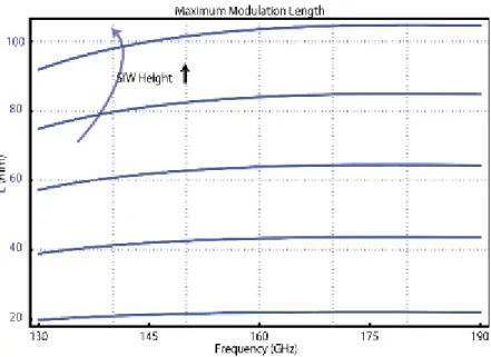
Figure 2.11: Calculated maximum length as a function of frequency for polymer SIW modulator. SIW width weff = 800 μm, height H changes from 10 μm to 50 μm. ... 33
Figure 2.12: Calculated maximum length as a function of frequency for polymer SIW modulator. SIW width weff = 800 μm , height H changes from 10 μm to 50 μm. ... 34
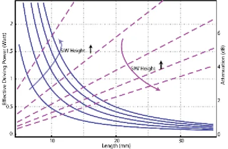
Figure 2.13: Calculated effective driving power as a function of active length for polymer SIW modulator; SIW width weff = 800 μm, NLO coefficient r=90 pm/V, and Height is changing 10
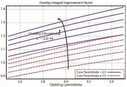
μm to 50 μm. ... 34 Figure 2.14: Overlap integral improvement factor as a function of cladding permittivity for polymer
SIW modulator. ... 37 Figure 3.1: A cross section view of mode-selective transmission line (MSTL). ... 51 Figure 3.2: Fields and current distributions in a typical MSTL. In frequency region I, MSTL works
under a mode with characteristic similar to TEM mode. In region II, MSTL operates under a mode with characteristic similar to TE10 mode. ... 52
Figure 3.3: A schematic of MSTL and its principle of operation: the conductor configuration leads the structure to operate under the TEM mode in lower frequency range and changing gradually to TE10 mode in higher frequency range. ... 53
Figure 3.4: a) Effective dielectric constant of MSTL (h = 50 µm, d = 12h, s = 0.8h, w = 3h), and comparison with effective dielectric constant of microstrip line TEM (h = 50 µm, d >>h, s>>h, w = 3h), and rectangular waveguide TE10 mode (h = 50 µm, d = 12h, s = 0, w = d/2) on
fused silica substrate (εr = 4.27). b) Group velocity of MSTL (h = 50 µm, d = 12h, s = 0.8h, w
= 3h), and comparison with effective dielectric constant of microstrip line TEM (h = 50 µm, d>> h, s>> h, w = 3h), and rectangular waveguide TE10 mode (h = 50 µm, d = 12h, s = 0, w
= d/2) on fused silica substrate (εr = 4.27). ... 54
Figure 3.5: Computed effective dielectric constant as a function of frequency: a) Slot width s as parameter, and εr = 4.27, h = 50 µm, d = 12h, w = 3h. b) Substrate thickness h as parameter,
and εr = 4.27, h = 50 µm, d = 12h, s = 0.8h. c) Computed effective dielectric constant as a
= 3h. d) Computed propagation loss as a function of frequency, waveguide width d as parameter, and εr = 4.27, h = 50 µm, s = 0.8h, w = 3h. ... 55
Figure 3.6: a) A fabricated sample line of MSTL on fused Silica substrate with a transition to picoprobe. b) A fabricated sample line of PCB prototype of MSTL with a transition to picoprobe. ... 57 Figure 3.7: Measurement setup. ... 57 Figure 3.8: a) Comparison of theoretical and experimental propagation phase constants (β) of
MSTL fabricated on fused silica (h = 50 µm, d = 12h, s = 0.8h, w = 3h). b) Comparison of theoretical and experimental propagation loss characteristics of MSTL fabricated on fused silica (h = 50 µm, d = 12h, s = 0.8h, w = 3h) and thin-film microstrip line from [45]. c) Gaussian pulse (Ref: 1ps FWHM) propagation on PCB prototype pf MSTL line and bend as well as comparison with that of microstrip line- I: MSTL line (10mm long) from theoretical calculation, II: MSTL line from experimental results, III: MSTL bend from experimental results, IV: microstrip line (10mm long, the same substrate as that of MSTL, and 50 Ω characteristic impedance) from ADS MoM simulation. ... 60 Figure 4.1: A cross section view of mode-selective transmission line. ... 71 Figure 4.2: Intended modes in MSTL with the dominance of vertical electric field components: a)
microstrip line mode, b) waveguide TE10 mode. ... 72
Figure 4.3: Equivalent transverse circuit network for MSTL in Fig. 1 with the reference plane in the middle of the slot s. ... 78 Figure 4.4: Propagation constant of guided-wave modes in MSTL using transverse resonance
method and comparison with the results of FEM method and theoretical calculation [36]. .. 78 Figure 4.5: a) Fields and current distributions in MSTL designed on quartz (h=50μm, d=12h, w=3h,
s=0.8h) from DC up to 0.5 THz range; fcutoff =120GHz, fmax=500GHz. In region I of frequency
range, MSTL works under a mode with characteristics very similar to that of TEM mode. In region II, MSTL operates with a mode with characteristics very similar to TE10 mode. b)
Effective dielectric constant of MSTL on quartz (h=50μm, d=12h, w=3h, s=0.8h) and comparison with effective dielectric constant of microstrip line TEM mode and rectangular waveguide TE10 mode. c) Group velocity of MSTL on quartz (h=50μm, d=12h, w=3h, s=0.8h)
and comparison with group velocity of microstrip line TEM mode and rectangular waveguide TE10 mode. ... 79
Figure 4.6: Calculated mode coupling characteristics of MSTL ... 80 Figure 4.7: MSTL cross section with MOL discretization for hybrid-mode analysis. ... 82 Figure 4.8: Calculated different sources of loss using the MoL, including radiation loss using the
HFSS package (MSTL with parameters εr=4.27, h=50μm, d=12h, w=3h, s=0.8h). ... 83
Figure 4.9: Comparison of calculated effective dielectric constant as a function of frequency using the MoL method and HFSS package; MSTL with geometrical parameters εr =4.27, h=50μm,
d=10h, w=3h, s=0.8h. ... 83 Figure 4.10: Computed effective dielectric constant as a function of frequency: a) Strip width w as
a parameter, and εr =4.27, h=50μm, d=12h, s=0.8h; b) Slot width s as parameter, and εr =4.27,
h=50μm, d=12h, w=3h; and c) Substrate width d as a parameter, and εr =4.27, h=50μm, w=3h,
s=0.8h. ... 84 Figure 4.11: Magnetic field and current distribution at 250GHz: a) MSTL, Magnetic field b) SIW,
Magnetic field c) MSTL, Surface current d) SIW, Surface current ... 85 Figure 4.12: Comparison of calculated propagation loss of MSTL and SIW as a function of
frequency for different waveguide width d, εr =4.27, h=50μm, s=0.8h, w=3h. ... 86
Figure 4.13: MSTL guiding design curves in w/h-d/h plane showing the useful design region of interest. ... 87 Figure 4.14: Ey distribution (along the x-direction) for the fundamental propagating mode in MSTL
(εr=4.27, h=50μm, d=12h, w=3h, s=0.8h). ... 87
Figure 4.15: a) Calculated effective dielectric constant as a function of frequency with substrate permittivity εr as a changing parameter, and h=50μm, d=12h, w=3h, s=0.8h; b) Computed loss
as a function of frequency with substrate permittivity εr as a changing parameter, and h=50μm,
d=12h, w=3h, s=0.8h. ... 90 Figure 4.16: a) Comparison of theoretical and experimental propagation phase constant (β) of
MSTL prototype fabricated on RT/duroid® 6002 laminates from Rogers Corp. (h=127um, d=20h, s=1.6h, w=2.4h), b) Comparison of theoretical and experimental propagation loss
characteristics of MSTL prototype fabricated on RT/duroid® 6002 laminates from Rogers Corp. (h=127um, d=20h, s=1.6h, w=2.4h) and thin film microstrip line from ref [37]. ... 91 Figure 4.17: a) Comparison of theoretical and experimental propagation phase constant (β) of
MSTL prototype fabricated on quartz (h=50um, d=12h, s=0.8h, w=3h); b) Comparison of theoretical and experimental propagation loss characteristic of MSTL prototype fabricated on quartz (h=50um, d=12h, s=0.8h, w=3h) and thin film microstrip line from ref [39]. ... 92 Figure 5.1: a) Mode-selective transmission line (MSTL) on a dielectric substrate. b) MSTL with
TEM regime at lower frequency range (d>λg/2): electric and magnetic field distribution over the cross section and top view of magnetic field along the length of MSTL. c) MSTL with TE10 regime at higher frequency range (d<λg/2): electric and magnetic field distribution over
the cross section and top view of magnetic field along the length of MSTL. ... 103 Figure 5.2: MSTL interconnect design curves (the mode-conversion frequency cutoff) for different
values of substrate dielectric constants (εr =3, 4, 6, 9, 11) ... 104
Figure 5.3: Parametric study to optimize GVD over DC to 1 THz: thickness (h), strip width (w), slot width (s). ... 106 Figure 5.4: a) Fabricated MSTL line; b) Fabricated MSTL bend. ... 109 Figure 5.5: a) Comparison of theoretical and experimental propagation loss obtained from
frequency domain characteristics of the MSTL prototype fabricated on RT/duroid® 6002 laminates from Rogers (h=127um, d=20h, s=1.6h, w=2.4h) and its corresponding microstrip line from ref [27]. b) Frequency domain characterization of MSTL 90° bend. ... 109 Figure 5.6: Comparison of signal overshoot vs rise time between microstrip line and MSTL. .. 111 Figure 5.7: Gaussian pulse (Ref: 1ps FWHM) propagation on MSTL line and bend and comparison
with microstrip line. I: MSTL line (10mm long) from theoretical calculation, II: MSTL line from experimental result, III: MSTL bend from experimental result, IV: microstrip line (10mm long, the same substrate as MSTL, and 50 ohm characteristic impedance) from ADS simulation. ... 112 Figure 5.8: a) Rectangular pulse (50 ps width, 1ps rise time) after propagating 10mm through
microstrip line and MSTL. I: microstrip line—5 ps rise time and prepulse distortion, 20% overshoot, 18% backswing. II: MSTL, following the same rise time as the reference pulse,
6% overshoot, 8% backswing. b) Time domain characterization of RF/microwave signals: 2ps width, 0.1ps rise time via 1-cm-long MSTL, and comparison with the simulation of conventional 1-cm-long MTL. ... 112 Figure 5.9: Eye diagram fed from a pseudo random bit sequence NRZ signal source generator with
a 100-Gb/s data rate and 0.5ps rise time: a) MSTL and b) Microstrip line. ... 114 Figure 5.10:.Fabricated circuit for crosstalk measurement. ... 116 Figure 5.11:.Crosstalk measurement between side by side MSTLs. ... 116 Figure 6.1: A schematic of computational electromagnetic (CEM) simulation involved with
numerical calibration techniques. ... 127 Figure 6.2:. A transmission schematic representing a THRU simulation in a generalized calibration
procedure. ... 128 Figure 6.3:. a) Network flow graph of a generalized TT calibration. b) Network flow graph of a
THRU simulation in the proposed TT calibration. ... 130 Figure 6.4: Two-port network equivalence: a) Z-Network and b) Y-Network. ... 135 Figure 6.5: TEM/quasi-TEM mode transmission lines: a) CPW, b) Microstrip line; non-TEM mode
transmission line, c) SIW, and d) fin-line. ... 137 Figure 6.6: Comparison of the calculated TEM transmission line characteristic impedance using
the proposed TT numerical calibration technique, direct calculation from HFSS S-parameter, with experimental results from the literature: a) Amplitude or real part of Z0; b) phase of Z0 - I: CPW transmission line w=73 μm, s= 49 μm, wg= 250 μm on a fused silica substrate [23], II: Microstrip transmission line of 1.3 mil copper, w=0.1-in on an h=0.25-in alumina substrate [13], III: CPW transmission line of 0.5683 μm gold, w=71 μm, s= 49 μm, wg= 250 μm wide ground planes on an h=500 μm gallium-arsenide substrate [24], IV: CPW transmission line of 0.7 μm gold, w=73 μm, s= 49 μm, wg= 350 μm wide ground planes on a 500 μm gallium-arsenide substrate [25], V, VI: Microstrip transmission line of 1.3 mil copper, w=0.25-in, 0.5-in on an h=0.25-0.5-in alum0.5-ina substrate [13]... 138 Figure 6.7: Comparison of the calculated non-TEM transmission line propagation characteristics
S-parameter, and experimental and numerical results from the literature a) fin-line w=18mil, h=10mil in WR28, b) SIW a=4.8 mm on a h=1.5mm 2.2 permittivity substrate. ... 139 Figure 6.8: The distributed equivalent-circuit model (all elements are defined per length). ... 140 Figure 6.9: Calculated SIW characteristic of the first three modes (substrate εr=2.33 and 0.254 mm
thickness, width=0.711 mm) using the proposed TT method: a) characteristic impedance, b) effective dielectric constant. ... 141 Figure 6.10: Calculated characteristic impedance for SIW of Fig. 5(c) (substrate εr=2.33, a = 6.096
mm) for different substrate thicknesses using the proposed TT method including and excluding loss in the calculations a) real part of characteristic impedance b) imaginary part of characteristic impedance, c) The phase constant, d) attenuation constant ... 142 Figure 6.11: Calculated SIW interconnect parameter (substrate εr=2.33, width = 6.096 mm) for
different substrate thicknesses using the proposed TT method including and excluding loss in the calculations a) L (mH.s-1/m) b) R (Ω) b) C (mF.s-1/m) d) G (S) ... 143
Figure 6.12: A schematic of two types of ports and their principles of operation a) lumped port and b) wave port. ... 146 Figure 6.13: Wave port de-embedding in Ansoft HFSS. ... 147 Figure 6.14: Basic definitions of different impedance in a transmission line: a) input Impedance b)
characteristic Impedance ... 149 Figure 7.1: Cross-sectional view of CBN rib waveguide ... 157 Figure 7.2: Cross section of a rib waveguide ... 157 Figure 7.3: Simulated critical W/H ratio as function of the CBN thin film thickness H for various
values of r at λ = 1.55 μm in an SiO2-CBN-MgO rib waveguide structure. ... 159 Figure 7.4: SEM image of a 10% etched 2um epitaxial CBN thin film with 1µm SiO2 deposited
by PECVD. ... 161 Figure 7.5: Characterization setup with lensed fiber input (~2um spot size and ~50um working
Figure 7.6: Simulated (in color) and experimentally (in grey) measured mode profiles of SiO2-CBN-MgO rib waveguide structure with 2 μm CBN thickness, etch depth ~10% of CBN thickness and various rib widths. ... 163 Figure 8.1: Complete three-dimensional model of the SOI grating-waveguide device is considered
in this paper in both simulation and fabrication. In the simulation, half of the structure with shorter taper and waveguide length is simulated. ... 173 Figure 8.2: 3D Simulated structure. Half of the device is simulated using the wave port excitation
of the waveguide and the radiated beam is monitored. ... 174 Figure 8.3: The simulated radiation pattern of the proposed SOI grating coupler optimized to work
at 1550nm wavelength for the different grating periods. SOI wafer (260nm silicon layer and 2µm buried oxide), waveguide width 500nm, grating width 12.5μm, etching depth 70nm, and taper length 650μm. Coupling angle is changed with the grating period... 175 Figure 8.4: Simulated efficiency versus incident angles for the proposed SOI grating coupler at
1550nm wavelength for the different grating period. SOI wafer (260nm silicon layer and 2µm buried oxide), waveguide width 500nm, grating width 12.5μm, taper length 650μm, and etching depth 70nm. ... 176 Figure 8.5: Simulated efficiency versus incident angle for the proposed SOI grating coupler at
1550nm wavelength for different grating etching depth. SOI wafer (260nm silicon layer and 2 µm buried oxide), waveguide width 500nm, grating width 12.5μm, taper length 650μm. a) grating period = 580nm, b) grating period = 600nm. ... 177 Figure 8.6: Simulated efficiency versus incident angle for the proposed SOI grating coupler for
different wavelengths. SOI wafer (260nm silicon layer and 2 µm buried oxide), waveguide width 500nm, grating width 12.5 μm, taper length 650 μm, grating period 580nm, etching depth 70nm. ... 178 Figure 8.7: AFM scan of a grating coupler. ... 178 Figure 8.8: Measured efficiency of SOI grating coupler (260nm silicon layer and 2 µm buried
oxide, 580nm grating period and 70nm etching depth) at 1550nm wavelength and comparison with the simulation ... 179 Figure 10.1: A schematic of the proposed MSTL photoconductive switch. ... 188
LIST OF SYMBOLS AND ABBREVIATIONS
2D Two-Dimensional3D Three-Dimensional 5G Fifth Generation
ADI Alternating Direction Implicit BW Bandwidth
BPM Beam Propagation Method CBN Calcium Barium Niobate CEM Computational Electromagnetic CPW Coplanar Waveguide
DUT Device-Under-Test EM Electromagnetic
EBL Electron-Beam Lithography EO Electro-Optical
FEM Finite Element Method FIT Finite Integration Technique FWHM Full Width at Half Maximum GSG Ground-Signal-Ground ICP Inductively Coupled Plasma –
ICT Information and Communications Technology I/O Input/Output
IC Integrated Circuit
MZI Mach-Zehnder Interferometer MoL Method of Lines
MoM Method of Moments MSL Microstrip Line mmW Millimeter-Wave
MSTL Mode-Selective Transmission Line NC Numerical Calibration
OE Opto-Electronic OE Optoelectronics
PMPW Parallel Metal Plate Waveguide PCB Printed Circuit Board
RF Radiofrequency
RW Rectangular Waveguide RIE Reactive Ion Etching SOC Short-Open Calibration SOI Silicon-on-Insulator
SUS Structure-Under-Simulation SIC Substrate Integrated Circuit SIW Substrate Integrated Waveguide SoC System-on-a-Chip
SoP System-on-a-Package THz Terahertz
TTB Tetragonal Tungsten Bronze TRL Thru-Reflect-Line
TE/TM Transverse Electric/Magnetic TEM Transverse Electromagnetic
TR Transverse Resonance
ULSI Ultra Large-Scale Integration VNA Vector Network Analyzer VLSI Very Large Scale Integration
CHAPTER 1
INTRODUCTION
Overview
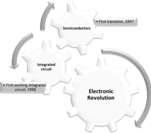
Two well-established key technologies, namely semiconductor materials and integrated circuit design, have inspired the electronics revolution in the 20th century and beyond (Figure 1.1). Utilizing semiconductor material, the transistor was invented at Bell Telephone Laboratories in 1948 in the context of a long distance communication [1]. After developing the first integrated transistor, Jack Kilby’s idea of the integrated circuit (IC) was born and the first working IC was demonstrated in 1958 [2]. From then on, applications of electronics have expanded dramatically thanks to a possible mass manufacturing of low-cost integrated circuits. Integrated circuits are used in almost all electronic equipment today. Computers, cell phones, smartphones, and other similar devices that are now inseparable parts of the structure of modern societies have been made possible through the development of low cost ICs.
With ever-increasing demands for global communication systems, the field of photonics came into a common use in the 1980s. Playing a complementary role to electronics, the applications of photonics have continued to emerge alongside. Thereupon, the revolutionary transition from old-fashioned teletype machines to the personal computer, computer networking, cell phones, and the World Wide Web all happened in less than four decades. All these technologies have been focused on communicating information at ever-increasing speeds, which are expected to continue to get improved and accelerated [3].
Recently, IEEE committees have declared that the bandwidth demand is growing faster than the current capacity to deliver it [4]. More than 44% of the world’s population is estimated to be online at this time and this percentage will grow up [5]. More users and more devices generate more bandwidth demand. In addition, terahertz (THz) and millimeter-wave (mmW) bands have attracted huge interest in recent years, from both the research and industrial communities, due to their wide and unique applications in many areas, such as security, scientific imaging, radars, space communications, medical diagnosis, and wireless systems [6]–[8]. THz applications in the information and communications technology (ICT) sector hold plenty of potentials to enhance the speed and capacity of communication and sensing networks. Currently, this fundamental and urgent need depends on how far innovative ICT devices are developed over such bands [9].
There is a strong virtuous circle encompassing advanced computing tools and better quality networking and information, subject to transmission speed or electrical signal frequency. As frequency increases, signals can carry more information resulting in improved computation speed and communication bandwidth. Nevertheless, there are some crucial bottlenecks, thereby restricting the development of both computing and telecommunication systems toward higher frequency as signal propagation and switching speeds in the electronic domain are inherently limited. Drawing an analogy to the electronic revolution and its fundamental elements, it is perceived that the first key to the success of electronic-photonic technology was the progress achieved in finding and fabricating high-performance and cost-effective optical and electro-optical materials. However, low cost and high performance design of THz and mmW integrated circuits is still a critical challenge.
Figure 1.1: Schematic representation of electronic revolution and its driving technologies.
Motivation
In 2010, the booming volume of data transmitted around the globe rendered the standardization of the 100 Gb/s Ethernet and 100G optical transport network, and still now higher rate interfaces are pushing research and industry toward exploring 400G as well as Terabit Ethernet [10]. On the other hand, increasing data rate in wireless communications pushes the transformation of radiofrequency (RF) technology toward a high mmW and THz frequency region as the fifth generation (5G) wireless communications technology is just on the horizon.
With rise and fall times around 100 psec, wire interconnects were transformed to transmission lines [11]. Integrated transmission lines in the form of microstrip line, coplanar waveguide (CPW), and their derivatives have been the backbone of modern electronic and photonic integrated circuits and systems. Following the evolution of IC technologies and processing techniques in the field, those fundamental structures have been continuously studied and improved to meet the constantly
Figure 1.2: History of transmission line: with increasing edge speeds, wires have been replaced with TEM transmission lines.
updated bandwidth and capability requirements. The planar transmission lines are the foundation of any high frequency ICs such as RFICs and MMICs, whose performance factors and cost indices are first limited by the transmission line building elements. Countless electromagnetic applications from DC to THz [9], and also growing needs for faster data communication rates have raised the question of whether traditional transmission lines can satisfy the demand of sophisticated applications for high performance [12]–[14] (Figure 1.2). Currently, the increase in bandwidth related to ultra-high-speed wireline digital computing systems, such as memory chips, CPUs, GPUs, backplanes, and wired LANs, are enabled by increasing the number of input/output (I/O) channel interconnects on chips [15]. To keep up with bandwidth demand and to avoid prohibitive cost and complexity, fast time-domain pulse signals would require the bus lines or interconnects design to support low-loss and low-dispersion signal transmission from DC to the mmW spectrum, and even up to THz bands if pico-pulsed signals are used. On the other hand, in wireless applications, although radio-over-fiber techniques are applied and high-density modulation schemes are used, available radiofrequency bandwidth is still relatively low [15]. In this case, the challenges are in pushing the use of radiofrequency signals toward the frequency range of mmW and higher [16], necessitating the development of ultra-high-speed electro-optical devices such as modulators and photodetectors, for which high performance DC-to-mmW/THz “electronic” transmission lines and interconnects are needed for integrated “electrodes” [17], [18].
With regard to the explosive Moore’s law and beyond [19] and the increasing trend in test cost for each new generation of chip manufacturing, new concept devices and circuits should be introduced to translate the recent achievements in finding and fabricating new high performance materials [20] and to enable the next generation of mmW and THz photonics applications in computing and telecommunications. Efforts have been made to evolve and improve the existing transmission line structures through the modification of current waveguiding structures, but the ultimate scientific and technological challenge necessitates the emergence of a revolutionary or disruptive concept in doing so. It is of great importance for us to establish a robust transmission line structure that enables the development of all-frequency integrated circuits from DC to THz, based on a single design and development platform.
Millimeter-wave photonics
In the late 1970s, experiments were initiated in order to take advantages of photonic technologies in microwave systems to accomplish the tasks that were deemed very complex or even impossible to perform entirely in the RF domain. Following that thread, the field of microwave photonics has been built up as an interdisciplinary field connecting radiofrequency (RF) and optoelectronics engineering worlds, and expanded in a way that microwave engineering techniques are also used to improve the performance of photonic communication networks and systems [21], [22].
Implementing mmW radio in backhaul networks and taking the desired advantages of THz-band wireless systems have encouraged the development of high performance mmW and THz photonic links. Wireless expansion of the next generation broadband access fiber optic networks, Gigabit Ethernet, and multigigabit communication systems is very promising and attractive in the form of a radio-over-fiber approach, enabling the easy transmission and delivery of mmW and THz signals over a long distance via low-loss optical fibers. However, their performance in terms of speed and capacity is closely linked to that of the devices on which they are based, as they should be supported by ultra-broadband devices and circuits on both the electronic and photonic sides.
To date, conventional available microwave structures are associated with advanced modulation schemes and signal-processing technologies to accommodate the required bandwidth, but available bandwidth is still relatively narrow in wireless applications. The fact is that the rate at which microwave integrated circuits have been improved has been unparalleled in the current countless applications of mmW and THz, and the key to accelerating the use of microwave photonics techniques in up-to-date real world systems is to improve the RF performance of microwave photonics devices. In other words, a particular challenge in this connection is to improve the RF spectral region of operation in these devices and to push the use of RF signals toward the frequency range of mmW and higher, while at the same time reducing cost [21]. High performance transmission lines are essential for improving microwave photonic applications, since traveling-wave-based structures are the key elements of guided-wave electro-optical and optoelectronic devices and circuits [20], [21]. As conventional TEM-mode structures are applied as the driving traveling-wave structure in EO devices, they suffer from extremely high loss at higher frequencies, and pose a limitation on high frequency performance. In addition, millimeter-wave and THz modulators with conventional TEM-mode electrodes introduce a great challenge in the packaging
of the modulator structures, which has also limited the use of those structures over such a frequency range. This is because of their unbounded signal transmission. Similarly, the most common method for producing THz bandwidth electrical signals in integrated circuits and devices is through optoelectronics. However, current conventional transmission lines fail to accommodate the picosecond electrical pulses generated by OE switches, and these pulses with several hundred gigahertz bandwidth fade and disperse within a few millimeters of propagation [23]. Moreover, in optical network communications, global RF interconnects are used ubiquitously in almost all chip-to-chip and module-to-module interfaces.
Terahertz electronic
Realizing THz electronics or establishing compact, high-performance electronic circuits that operate at THz frequencies, necessitates the conception and development of electrical and electronic devices as well as integration technologies that can operate at frequencies above 1 THz. Currently, limitations in transistor performance have been addressed to a great extent, making it possible to drive solid-state electronics directly at these frequencies. Whereas the first high-frequency transistor, developed in 1953, was capable of operating up to 60 MHz, with the advances in transistor technology, fmax above 1 THz has already been demonstrated [24], [25] and a single
device switching time has been reduced to 2 picoseconds or less [26]. By increasing the transistor speed, on-chip interconnects, although keeping the same structure, become even denser. In 1995, Intel declared, “on-chip interconnect scaling has become the real limiter of high-performance integrated circuits” [27]. In 1992, personal computers were equipped with Intel 486, clocking 66 MHz; CPU clock speed increased and soon passed 500 MHz, and continued upward. However, in 2005, the top speed of the high-end processors resided around 4 GHz and since then, improving the speed has been accomplished through applying multi-core processors. The well-known bottlenecks related to high-speed digital and/or broadband analog signal interconnects, for example, have been the primary limitations to various integrated circuits and systems with respect to their loss- and dispersion-limited performance. This creates a strong motivation to search for super wideband transmission lines and make related discoveries and innovations [9], [12]–[14]. On-chip interconnects in such a high frequency are increasingly becoming the major bottlenecks and greater performance limiters of system-on-a-chip (SoC) and system-on-a-package (SoP) than transistors [29]–[31]. Ultrahigh-speed pulse transmission (covering the DC-THz range) requires
transmission lines with low dispersion and low loss, which can be readily integrated into optoelectronic circuits and other devices [32].
Objective
The overall objective of this thesis is to establish a new platform in integrated electronic and photonic circuits and systems to bridge the gap between electronics and photonics. From this overall goal, three detailed objectives are identified as follows:
1) To propose novel EO and opto-electronic (OE) devices based on non-TEM mode integrated transmission lines for mmW and THz applications as well as the design and full study of an SIW EO modulator as an example;
2) To design, devise and demonstrate a low-loss low-dispersion transmission line for DC to THz frequency spectrum, and to demonstrate an interconnect prototype for THz electronic applications; and
3) To design and demonstrate optical waveguides and optical grating couplers based on novel high-performance EO material applicable to mmW and THz.
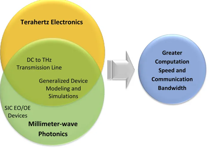
In the long term, this work is intended to establish a groundwork for the interdisciplinary field of terahertz electronics and photonics and a breakthrough offering the promise of greater computation speed and communication bandwidth (Figure 1.3).
Methodology and contributions
Non-TEM mode electro-optical modulator for mmW and THz
applications
A fundamental challenge in optical telecommunication is to modulate mmW or THz bandwidth, or simply carrier signals, onto an optical wave carrier in phase and/or amplitude, depending on broadband communication services. This is usually accomplished with an external EO modulator, varying either the intensity or the phase of a light emitted by a laser diode. EO modulators are utilised in a variety of ways. At millimetric scale, they can be employed to adapt an optical channel to carry information such as telephone calls and digital data for network transmissions. At micrometric scale, they can be used to interconnect chip microprocessors in multi-core systems. In
either case, these devices modulate a light beam carrier through an RF modulating signal, inserting data to be sent to the receiver side. A high-frequency EO modulator is critical in enabling signal processing and distribution in next generation cloud computing, telemedicine, and telecommunications.
To achieve this, a great deal of research has been conducted on molecular engineering of electro-optically active materials and cladding material properties to improve overall device performances. Novel organic EO materials enhance the EO modulator response to the point that high bandwidth polymer modulator designed for the 100G optical communications channel is now commercially available [33]. Thanks to an excellent velocity match between the modulating signal and lightwave in polymers, this device must be able to operate within an ultra-broad bandwidth. However, in the conventional device structure of EO modulators, the driving power is applied through the microstrip line, which plays the role of metal electrodes. This kind of transmission line is significantly lossy for high-frequency operations.
The modulator structure can be modified so that the electrical driving power is controlled by an appropriate transmission line, which is applicable in high frequency operation. The purpose of this work is to design, develop, and realize a novel EO modulator structure based on substrate integrated circuit (SIC) technology. In this project, substrate integrated waveguide (SIW) is exploited as an alternative fundamental transmission line structure in support of electrical signal for the design and development of mmW and THz traveling-wave polymeric EO modulators. Supporting theoretical development and modeling results are established to validate the concept. The proposed theoretical model for traveling-wave operation together with optical simulation provides an efficient approach that will specify the values of various parameters in order to obtain the optimized EO modulator design. This technology may lead to a whole new generation of ultra-high-speed EO modulators with more than 100 GHz modulation speed. Such SIW-based EO modulators may play important roles in enabling RF photonics and next generation higher-bit-rate optical fiber communication systems [17].
Devising and demonstrating low-loss and low-dispersion transmission
lines
Transmission lines are the building blocks of all electronic and photonic integrated circuits and systems. In spite of a substantial expansion of electronic and photonic applications toward THz, the basic structure of traditional transmission lines, developed in the 1950s, has yet to be modified. One of the fundamental bottlenecks in the development of THz integrated electronic and photonic systems has been the intrinsic limitations of those conventional transmission lines. Incremental efforts have been made to evolve and improve existing transmission line structures to meet the increasingly stringent demands for signal transmission bandwidth and performance. However, the inherent structural metal configuration is still the dominant obstacle dictating a particular operating mode that is prone to attenuation and dispersion at higher frequencies. A potentially revolutionary scheme or disruptive concept is required in support of future technological needs and bridging the gap between electronics and photonics.
There are two categories of waveguiding structure, namely, the transverse electromagnetic (TEM)-mode type, such as microstrip lines, and transverse electric/magnetic (TE/TM)-(TEM)-mode type such as SIW. TEM structures support the transmission of signal from zero frequency (DC), but they experience increasing signal attenuation and dispersion at mmW and THz frequencies. The current transmission lines used in electronic integrated circuits operate under the fundamental TEM mode. They suffer from inherent drawbacks such as strong signal attenuation and pronounced modal dispersion at room temperature, and they cannot be useful over a broad frequency range from DC to THz or ultra-high-speed pulse transmission. TE/TM structures, on the other hand, support the transmission of those high frequency signals but cannot cover DC and low frequency signals, and they are dispersive because of cut-off frequency.
In this work, a class of transformative transmission lines and waveguides are devised and demonstrated. The so-called “mode-selective transmission line” or simply MSTL, supports a dominant mode very similar to the microstrip line scenario in lower frequency range covering DC, while it is automatically reconfigured to support the fundamental mode of rectangular waveguide at higher frequency [34], [35]. This “smart” transmission line, effectively covering the desired operation from DC to THz frequency range, is suitable for full DC-THz electromagnetic propagation and ultra-high-speed THz pulsed signal transmission. It can be made to support a
single-mode transmission over a super-wide range of frequency. This MSTL, in a fully integrated form, exhibits a disparate modal characteristic of traditional planar microwave transmission lines and non-planar metallic waveguides. Whereas at low frequency MSTL operates under the TEM regime, the operating mode is gradually converted to low-loss TE10 mode for operation at high
frequencies, such as millimeter-wave and THz. This approach allows for the possibility of developing densely integrated interconnects and planar guided wave structures for DC-THz bandwidth [28], [29].
During the course of this PhD project, a unified method will also be introduced and formulated for deriving the equivalent circuit model of a two-port network and the characteristic impedance of a transmission line or waveguide for any mode [40]. This method is devised through the combination of a multimode calibration and a commercial numerical simulator. It is based on a generalized calibration technique, which is applicable to the case of TEM mode as well as non-TEM and higher-order propagating modes. The method is simple and straightforward, without any complication in the calculations or limitation in the operating frequency.
Application in mmW/THz photonics
MSTL can be exploited as an alternative fundamental transmission line structure in support of RF electrical signal for the design and development of mmW and THz photonics devices. Two central applications are in an optoelectronic photoconductive switch for THz pulse generation and an electro-optic Mach-Zehnder modulator.
Photoconductive switching has been the most common method for producing THz bandwidth electrical signals in transmission lines throughout integrated circuits and devices. Ultrafast electrical pulses (DC-THz range) require transmission lines with low dispersion and loss, which can be readily interconnected to optoelectronic and other devices. A major problem in transmission lines for ultrafast electrical pulses is dispersion, since it causes pulse broadening and loss of speed [23]. Several theoretical analyses of this dispersive broadening of pulses on microstrip line and coplanar waveguide show that a strong dispersion exists in these transmission lines, especially when the pulse rise time is short (e.g., tens of picoseconds). To solve this problem, conventional transmission lines are replaced with MSTL to insure low-loss and low-dispersion THz bandwidth pulse propagation. On the other hand, for EO modulator, finding an appropriate scheme for applying mmW/THz waves to the lightwave channel has been a particular problematic issue. To
address this problem, applying MSTL serves as the traveling wave structure, providing low loss and low dispersion characteristics. This work proposes using organic nonlinear EO polymer material, due to its intrinsic material bandwidths, high EO coefficients, easy processability, and integrability with semiconductor VLSI electronics and silica fiber optics, and potential for low cost. In this structure, the velocity mismatch is minimized and can easily be controlled. Therefore, in wireless communications, carrier frequency will increase to the point that bandwidth is wide enough to achieve a large data capacity even with a simple modulation technique. Furthermore, this EO modulator is a key element for improving the performance of opto-electronic oscillators. Such THz photonic integrated circuits would help to close the THz technology gap between microwave electronics and infrared photonics. This research would result in the development of next generation high-frequency performance-demanding mmW/THz photonic integrated circuits and systems.
Application in THz electronics and on-chip interconnect
MSTL allows for the possibility of developing densely integrated interconnects and planar guided-wave structures for DC-THz bandwidth applications. To increase bandwidth related to ultra-high-speed wireline digital domains or computing systems, each set of existing input/output (I/O) channels would be replaced by a single ultra-wideband MSTL interconnect. This loss, low-dispersion broadband integrated transmission line is a key enabling disruptive technology towards the development of the next generation of DC-to-THz integrated electronic circuits and systems. Additionally, this concept points out a self-packaging solution that is necessarily required for THz and mmW integrated circuits, as it is anticipated that unavoidable dielectric loss and insufficient patterning accuracy may limit the use of current packaging techniques for mmW and THz-wave applications.
Design and demonstration of the optical waveguide and modulator based
on CBN
Calcium barium niobate (CBN) is a new EO material in the form of thin films [41], [42]. These films exhibit a high Curie temperature (>50 °C) that ensures thermal stability. It was also shown that the CBN film EO coefficient (r33 as high as 130 pm/V) is more than 4 times higher than that
being integrated in a silicon platform. The deposition, structural characterization, and fabrication of this material stack can be found in [44]–[46].
Although the operation of waveguide devices is well studied and understood, their particular performance relies on many parameters, such as geometry, wavelength, initial field distribution, material data, and electro-optic driving conditions. These parameters must be optimized before fabricating a device. In this work, a CBN-based low-loss optical waveguide is designed and demonstrated as the first step to realizing a CBN-based EO modulator [46]. The optical design of a static CBN electro-optic is also prepared. Simulation parameters are based on the corresponding achievements in the fabrication process of growing and etching CBN, which is a completely novel unexplored electro-optic material. Simulations are carried out based on Beam Propagation Method
Terahertz Electronics
Greater
Computation
Speed and
Communication
Bandwidth
Millimeter-wave
Photonics
DC to THz
Transmission Line
Generalized Device
Modeling and
Simulations
SIC EO/OE
Devices
Figure 1.3: Terahertz electronics and millimeter-wave photonics overlap and contribution of this thesis.
(BPM), applying commercially available software. BPM is a systematic method for simulating the passage of light through a waveguide medium in which the optical field can be tracked at any point as it propagates along the guiding structure. BPM is based on a numerical solution for an approximation of the Helmholtz equation, which governs light propagation in dielectric media. Refractive index distribution and starting propagation field (i.e., a waveguide mode in our case) are required for three-dimensional (3D) modeling. 3D BPM simulator is based on Alternating Direction Implicit (ADI) mode solver, in which the semi-vector algorithm provides a choice between quasi-TE and quasi-TM polarization.
Since end-fire coupling presents some difficulties in characterizing the CBN optical waveguide, a new approach for the design of an out-of-plane grating coupler is also established during the course of this PhD project [47]. A three-dimensional simulation of the grating coupler is performed for the first time, which enables a rigorous investigation of this periodic structure. Using the vector formulation of the Maxwell’s electromagnetic equations with a commercial software package in the context of a full-wave finite-element method, the power distribution diffracted by a grating (radiation pattern) is resolved and the grating efficiency is examined. A parametric study is performed to determine the dependence of the wave leakage on structural geometry, operating wavelength, and polarization as well as incident angle of the light. In addition, since the complex propagation constant (γ=α+jβ) cannot be obtained directly from the simulation, we have determined it through a numerical calibration method. A grating design involving Silicon-on-Insulator (SOI) wafer is optimized. Test structures with grating couplers and tapered strip waveguides are fabricated using a two-step electron-beam lithography and high-density plasma etching processes, and characterized showing an excellent agreement among theory, simulation, and experiment, fully validating the design method.
Thesis roadmap
This thesis is organized as follows:
Chapter 2: The concept of SIC EO modulator is introduced and SIW EO modulator is studied in detail [17], [18].
Chapter 3: The concept of MSTL is introduced and its principle of operation is discussed. The device is fabricated and characterized in both time and frequency domains [34], [36].
Chapter 4: Complete theoretical study is performed on MSTL and guided-wave properties are derived. A detailed semi-analytical hybrid-mode analysis is developed through the application of method of lines (MOL) and propagation characteristics in terms of dispersion, modal, and loss properties are examined, which leads to the establishment of some basic MSTL design guidelines and also an optimization approach [35], [37].
Chapter 5: MSTL is exploited as an alternative approach to accommodating the growing requirements of ultra-large-scale integration (ULSI) for density, performance, and bandwidth. A detailed parametric study is performed to optimize the MSTL structure for high-speed global interconnects and high-performance signal integrity [38], [39].
Chapter 6: A unified method is introduced and formulated for deriving the equivalent circuit model of a 2-port network and the characteristic impedance of a transmission line or waveguide for any mode. The method is verified for both TEM and non-TEM propagating mode and is applied to extract the characteristic impedance and circuit model of non-TEM guided wave structures [40].
Chapter 7: An electro-optical SiO2-CBN-MgO rib waveguide structure is designed. The
simulation, optimizations, and optical characterizations are included [46]–[48].
Chapter 8: A three-dimensional simulation of grating coupler is conducted, guided wave and leakage characteristics of an out-of-plane grating coupler are studied in detail, and the coupling efficiency is derived. The simulations are verified through characterization [49], [50].
Chapter 9: Details on the general discussion are given. Chapter 10: Conclusions and future work are discussed.
CHAPTER 2
ARTICLE 1 : BAND-PASS NON-TEM MODE
TRAVELING-WAVE ELECTRO-OPTICAL POLYMER MODULATOR
FOR MILLIMETER-WAVE AND TERAHERTZ APPLICATION
Overview: electro-optic modulator is one of the key components in optical communication systems. In an optical transmitter, the first step after light generation through a semiconductor light source is modulating the light to carry information. Because direct modulation of semiconductor lasers leads to frequency chirp, external modulation is used and Mach-Zehnder modulator is the most common one. To transform microwave photonics to mmW/THz photonics effectively, developing mmW/THz electro-optic modulator plays a critical role. Nonlinear organic optical material has the fastest electro-optic response rate and can be used in mmW/THz. This work presents an electro-optic polymer modulator in which the traveling-wave structure is substrate integrated waveguide (SIW). The operating frequency or data rate of such EO modulator is determined by the operating frequency of the utilized SIW structure.