HAL Id: tel-00449756
https://tel.archives-ouvertes.fr/tel-00449756
Submitted on 22 Jan 2010HAL is a multi-disciplinary open access archive for the deposit and dissemination of sci-entific research documents, whether they are pub-lished or not. The documents may come from teaching and research institutions in France or abroad, or from public or private research centers.
L’archive ouverte pluridisciplinaire HAL, est destinée au dépôt et à la diffusion de documents scientifiques de niveau recherche, publiés ou non, émanant des établissements d’enseignement et de recherche français ou étrangers, des laboratoires publics ou privés.
the micro- and the nanometer scales
Thierry Leichle
To cite this version:
Thierry Leichle. Bioplume : a MEMS-based picoliter droplet dispenser with electrospotting means for patterning surfaces at the micro- and the nanometer scales. Micro and nanotechnolo-gies/Microelectronics. Université Paul Sabatier - Toulouse III, 2005. English. �tel-00449756�
THESE
Préparée au
Laboratoire d'Analyse et d'Architecture des Systèmes du CNRS
En vue de l'obtention du
Doctorat de l'Université Toulouse III - Paul Sabatier
Spécialité
Matériaux, Technologie et Composants de l'Electronique
Par
Thierry Leïchlé
Bioplume: A MEMS-based Picoliter Droplet Dispenser
with Electrospotting Means for Patterning Surfaces
at the Micro- and the Nanometer Scales
Soutenue le 5 décembre 2006, devant le jury:
Président: Robert
PLANA
Directeurs de thèse: Christian
BERGAUD
Liviu
NICU
Rapporteurs: Anja
BOISEN
Rosaria
FERRIGNO
Examinateur: Juergen
BRUGGER
Une seule certitude suffit à celui qui cherche.
Albert Camus
Je n'offre pas ici une lecture d'amusement.
Indépendamment du sérieux du sujet, il demeure dans la façon dont il est traité, un air de désordre que je n'ai pas eu la force de corriger.
Acknowledgments
Je tiens tout d'abord à remercier mes directeurs de thèse: Christian qui m’a initialement offert ce merveilleux projet, et Liviu avec qui j’ai partagé cette formidable aventure scientifique et qui compte maintenant parmi mes amis. Je remercie également les membres de mon jury de thèse pour leurs nombreux commentaires constructifs et pour le temps précieux qu’ils m’ont accordé.
Je veux exprimer ma gratitude envers tous les membres du laboratoire et de ses services, qui font du LAAS un cadre de travail idéal et épanouissant. Je pense en particulier aux personnels des services II et TEAM sans qui rien de concret n’aurait été enfanté.
Merci à tous les acteurs et collaborateurs de ce projet: Fabrice, JB et Daisuke au LAAS, Christiane à l’AIME, Thierry, Pascal et Emeline au CEA, Miguel, Pascal et Andrea au JRC, Maryna au Tyndall National Institute, et Nathalie à la Plateforme. Je pense aussi aux partenaires du projet européen NaPa, et spécialement à tous les membres du MEMS-based nanopatterning subproject, avec qui j’ai vécu une expérience européenne inoubliable car enrichissante tant sur le plan scientifique que sur le plan humain.
Je veux aussi remercier toutes les personnes du laboratoire avec qui j’ai passé les bons moments de détente nécessaires à une vie équilibrée de chercheur: tous les cadres et étudiants de notre très cher groupe Nanobiosystèmes; ainsi que mes camarades de bureau et mes amis du café et du privé: Laeti, Paul, Cédric, Laurent, Mat, Chris, Mathieu, Habib… Que ceux que je n’ai pas cités m’en excusent…
Enfin mes plus chaleureux remerciements s’adressent à ma famille, mes parents et mes frères qui m’ont soutenu pendant toutes ces années d’études et qui ont sûrement attendu longtemps ce moment…
Thank you, Ann, for your patience, your support and your love.
The partial financial supports of the EC-funded project NaPa (Contract no. NMP4-CT-2003-500120) and the Nano2Life European Network of Excellence (Contract no. NMP4-CT-2003-500057) are gratefully acknowledged.
Table
of
Contents
Introduction ……….1
Chapter I - Surface Patterning at the Micrometer and the Nanometer Scales 1. Introduction ………6
1.1. Definitions - Notions on surface patterning ………...6
1.2. Benefits related to the size reduction ……….6
2. Applications ………8
2.1. Electronics.……….8
2.2. Photonics .……….10
2.3. Biotechnology and chemistry .……….11
2.4. Material and surface sciences .……….13
3. Characteristic elements and challenges….………15
3.1. Minimum resolution and feature size .……….15
3.2. Pattern uniformity and reproducibility of replicated patterns .………15
3.3. Combination of different feature sizes .………...16
3.4. Materials - Quality and functionality ………...16
3.5. Range and combination of materials ………...17
3.6. Substrate state and pattern alignments ……….17
3.7. Concluding remarks ……….18
4. Overview of the patterning tools and methods ……….18
4.1. Direct writing techniques ……….18
4.2. Self-assembly ………...21
4.3. Replication of patterns ……….22
4.4. The need for alternative patterning techniques ………...26
5. Liquid-based patterning tools ………...27
5.1. Ink delivery by non-contact methods ……….……….27
5.2. Ink delivery by contact methods ………..33
5.3. Summary ………..41
5.4. Toward a highly functional micro dispensing system: Bioplume ………...42
6. Conclusion ………42
References ………44
Chapter II - Implementation of the Bioplume Liquid Dispensing System 1. Introduction ………..49
1.1. Background ……….49
1.2. Presentation of the initial system ………49
1.3. Motivation for this work ……….50
2. Challenges and solutions ………..50
2.1. Monitoring cantilever position and contact time and force during deposition ………...50
2.2. Parallelization of printed materials ………..51
2.4. Active control during deposition with electro-assisted methods ………….52
3. Design and fabrication of the bioplume chip ………...53
3.1. Design of the cantilevers ……….53
3.2. Design of the bioplume chip ………58
3.3. Fabrication of the cantilever array ………...59
4. Piezoresistive cantilever measurement and characterizations ………..62
4.1. Readout electronics ……….62
4.2. Characterization of the piezoresistive cantilevers ………...66
4.3. Relation between the voltage output and the contact force during deposition ………68
5. Automated spotter in closed-loop configuration ………..72
5.1. Principle of operation ………..72
5.2. Positioning apparatus ………...72
5.3. Response of the piezoresistive cantilever array in the deposition configuration ………...74
5.4. Control of the positioning system using the piezoresistor response ……...75
5.5. Spotting procedure ………...78
6. Influence of deposition parameters on the uniformity and the size of the printed features ………78
6.1. Materials and methods ……….78
6.2. Experiments ……….79
6.3. Results and discussion ……….81
7. Loading and deposition tests for biological applications ……….82
7.1. Deposition of functional biomolecules ………83
7.2. Deposition of different molecules in a single run ………...87
7.3. Cantilever loading with electrowetting actuation ………88
8. Conclusion ………91
References ………93
Chapter III - Mix and Match Surface Patterning Methods for Active Control during Deposition 1. Introduction ………..95
1.1. Liquid delivery and self-assembly ………...95
1.2. Liquid delivery and electro-assisted methods ……….96
2. Local deposition of nanoparticles using bioplume ………...96
2.1. Introduction - Motivation for this work ………...96
2.2. Nanostructuring surfaces with conjugated silica colloids ………...97
2.3. Formation of crystals of polystyrene nanobeads ………...105
2.4. Conclusion ……….109
3. Electrochemistry and electrowetting in picoliter droplets ………..110
3.1. Control of the droplet size using electrowetting actuation ………110
3.2. Copper electrodeposition localized in picoliter droplets using microcantilever arrays ………...113
3.3. Fabrication of oligonucleotide chips using parallel cantilever-based electrochemical deposition in picoliter volumes ………..118
4. Conclusion ………..126
References ………..128
Prospective outlook
1. Further reduction of the spot size - Nanobioplume ………135
2. Proposed solution ………135
3. Fabrication process ……….136
4. Preliminary deposition tests with nanobioplume ………...137
5. Results ……….138
6. Conclusion ………..138
Introduction
Surface patterning consists in creating physical or chemical patterns on a substrate enabling differences in topographies, functionalities and surface properties. The process of drawing features exhibiting micrometer and nanometer scale resolutions is of great importance in modern science and technology. The invention of the solid-state transistor and the integration and the miniaturization of complex functions were possible thanks to an understanding and a control of the fundamental phenomena related to quantum physics and material science but also thanks to the development of reliable patterning tools for device manufacturing. This revolution that has already been effective in electronics, electro-optics and information technology (leading to powerful PCs, cell phones, or home electronics) is now starting to involve other scientific fields targeting all new applications. Because a multidisciplinary approach of science supported by technological breakthroughs is a key to study and understand life, new curing abilities will emerge (when technology helps us to live better) and new devices, more efficient and environmental friendly, will be designed and fabricated (when nature inspires technological advances). However, coupling biology and man-made systems raises two main technical issues: one is related to the chemical composition of the materials involved in both types of systems (organic versus mostly inorganic); the other one is the small size of the biological building blocks and entities (cells, DNA strands, or molecules) compared to the scale of the surrounding human world. In this context, surface patterning is foreseen to play a major role for the fabrication of hybrid devices and, as a result, will encounter numerous challenges. Size, resolution, uniformity, and alignment of the fabricated patterns are the main issues that are aggravated by the downsizing process. The cost of the techniques is not to be neglected and the writing speed and total covered area are important parameters when one thinks about industrial production. Giving the fact that all these issues can not be all addressed by a single tool, different techniques are now available.
The first surface patterning tool, the classical UV lithography process, has been initially developed to fabricate complex integrated circuit chips. However, because of its complexity and high cost, it is now not necessarily the most appropriate tool for the fabrication of simple novel devices such as, for instance, lab-on-chips or microlenses. Thus, lately, numerous techniques have emerged to propose solutions suited to specific applications. Generally there are two ways of patterning surfaces: by adding or by removing materials. In both ways, features can either be directly written or replicated from existing masters. Among the direct patterning techniques, some rely on the local delivery of liquids. Usually, liquids contain active species (i.e. biological molecules, nanoparticles, etching chemicals, and so on) consisting directly in the pattern feature, or
being part of an intermediate fabrication step. The currently existing tools address the millimeter and micrometer scales (pins, ink-jet printers) to the nanometer scale (dip-pen). However, creating patterns with 1 µm to 10 µm resolution is difficult because: i) it is time consuming using dip-pen and ii) other tools are too large, not precise enough or simply not mature at all.
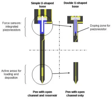
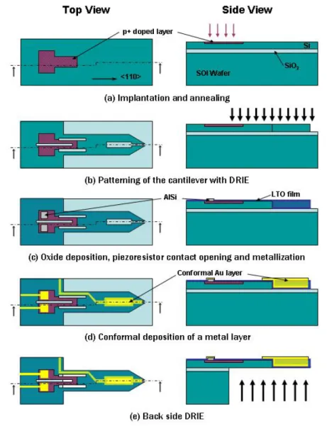
In this thesis we present a patterning tool that allows the creation of micrometer scale features by changing the physical and biochemical properties of surfaces from the local liquid delivery of reactants. This tool, so-called bioplume, consists of an array of 12 microfabricated silicon cantilevers directly inspired from the well-known fountain pen. Thus, each cantilever incorporates a channel and a reservoir in its tip to allow liquid delivery and storage, respectively. Droplets of liquid are formed onto the deposition surface by a direct contact of the cantilever tip and the surface. By adjusting the wetting properties of the tip and the surface, as well as the contact time, deposited drops exhibit diameters ranging from several micrometers to a hundred micrometers, corresponding to picoliter volumes. Displacement of the cantilever array is achieved by mounting the silicon chip onto a four-degree-of-freedom automated spotter. To enable a control of the contact force and time during deposition, force sensors are incorporated into the array by means of piezoresistances integrated into the silicon cantilevers. The array includes 10 depositing pens, allowing the parallelization of the deposition process. The homogeneity of the array of printed droplets is guaranteed by using the force sensors to control the trim of the array regarding the depositing surface. The cantilever array, the PC-controlled spotting system and the electronics dedicated to the piezoresistance measurements form a closed-loop system that enables the automatic displacement of the array and the overall control of the deposition parameters. By using a specific external loading chip, different liquids can be loaded onto the cantilevers, enabling the parallel deposition of several entities in a single deposition run. Besides, a gold electrode is incorporated in the channel to allow using electrowetting and electrochemistry. The former is used to actively load the cantilever or to control the drop size during delivery, while the latter is used to drive electrochemical reactions in the deposited picoliter droplets. This tool has been used to print different types of solutions containing DNA or nanoparticles, and materials (i.e. polymers and metals) onto various substrates. The control of the printed features (resolution, thickness, and composition), the versatility of the printed materials and the added electro-assisted features prove that this tool has a real potential for research work and industrial applications.
The first chapter of this thesis provides a brief introduction to surface patterning. After presenting specific applications related to different technological fields, the main tools are reviewed with a particular focus on the liquid-based patterning techniques. In the second chapter, the bioplume system is introduced. Design considerations focusing on the mechanical and electrical properties of the piezoresistive cantilevers are given. The fabrication process, relying on conventional microfabrication techniques that allow the realization of low-cost and disposable devices, is then detailed. The electronics and the automated spotter are briefly discussed as well as the closed-loop implementation. This chapter ends with the testing of the fabricated chips within the system to prove its functionality. The last chapter finally presents two interesting deposition features relying on the use of nanoparticles and electrochemical reactions, respectively. Firstly, the bioplume tool is used to directly pattern particles suspended in liquid media. The formation of perfect crystals located in the deposited drop is successfully achieved by tuning the surface wettability, the particle concentration and the solvent evaporation rate. Secondly, by means of an electrode incorporated into the cantilever channel,
electrochemistry is carried out inside the drop during deposition. The in-situ local electrodeposition of copper and the electropolymerization of polypyrrole are studied and presented to prove the spotter potential in this configuration. A final conclusion presenting the highlights of this work is provided at the end of this manuscript.
This work has been conducted within the European project NaPa (Emerging Nanopatterning Methods) of the Sixth Framework Programme (Priority 3 - NMP). The objective of NaPa is to provide a set of new methods to enable the transfer from nanoscience to nanoengineering. In particular, it proposes a solution to two general problems: i) the fast and efficient fabrication of nanodevices and ii) the low-cost replication of nanodevices enabling them to be generally available on the market. Thematically, the project embraces and pushes forward the state-of-the-art developments in the physical and engineering sciences with the object-driven mission to provide European industrial and academic researchers with a library of novel nanopatterning processes needed to underpin radical innovations and further scientific developments in nanotechnology. The NaPa consortium integrates well over 80% of the viable existing European know-how in the new patterning methods into a single integrated project. The project complements the deep UV technology by providing low-cost scalable processes and tools to cover the needs of nanopatterning from CMOS back-end processes through photonics to biotechnology. To achieve this, research in three technology strands are currently being carried out: nanoimprint lithography, soft lithography & self-assembly, and MEMS-based nanopatterning. Our contribution to this project belongs to this last category and aims at developing and bringing to a maturity level the microcantilever-based liquid dispensing tool originally proposed by our research group.
Chapter
I
Surface Patterning at the
Micrometer and the Nanometer Scales
The aim of this chapter is to give an overview of surface patterning at the micrometer and the nanometer scales with a particular focus on the tools that rely on liquid delivery.
After introducing general notions on surface patterning, such as basic definitions and advantages of reducing the feature size, some specific applications that can benefit from the breakthrough and the maturity of the patterning technologies are explored. The important parameters used as characterization elements and the issues inherent to the quality control of the printed patterns are discussed. These characteristics and challenges are:
- Minimum resolution and feature size
- Uniformity and reproducibility of the replicated patterns - Combination of different feature sizes
- Quality and functionality of the deposited materials - Range and combination of materials
- Substrate state and pattern alignment
With these elements in mind, the different classes of techniques are briefly listed and described. These categories include the direct writing, the self-assembly and the replication of patterns. Details are given concerning the ink-based tools that use an external liquid source to create patterns or to locally functionalize surfaces by add-on processes or etching techniques.
The choice of focusing this chapter on tools is deliberately made because new devices and ideas are believed to emerge from technological breakthroughs even though technology is application driven. Indeed, the conventional microfabrication tools (for instance masks and aligners for photolithography, or reactive ion etching (RIE) equipment) that have initially been developed for the microelectronics industry later on rendered possible the invention of microelectromechanical systems (MEMSs). The emergence of MEMSs has successfully provided new systems, such as accelerometers used in the automotive industry or ink-jet heads for printers, targeting applications that could not have been envisioned without mature fabrication tools.
1. Introduction
1.1. Definitions - Notions on surface patterning
Surface patterning is a process resulting in printed features on a substrate. The patterns consist of differences in layer topography, differences in surface properties, or most often a combination of both structural and functional modifications.
Topography, defined as the variations in thickness of a layer, can be tuned by adding material or by partially or fully removing the layer. This type of surface structuration can either be used as a step in a fabrication process (the patterned layer serves as a mask for subsequent etch or deposition processes), as a mechanical constituent of a device, or as a direct way to change the final physical properties (usually mechanical or optical) of the area onto which the building-block features are replicated and arranged periodically.
Surface functionalization results in a local alteration of the physical, chemical or biological properties of a surface. The modification of the surface state is usually achieved by working with magnetic or dielectric materials, polymers, chemical monolayers or biomolecules. Each patterned entity exhibits a specific property and the parallelization of the patterns can lead to additional functionalities.
Hence, desired surface properties can be obtained by playing with the shape of the basic feature, the repetition drawing and the type of patterned materials. Being able to combine different physical and biochemical functions on different areas of a same surface is a key to the fabrication of complex devices, for example sensor arrays with high sensitivity and selectivity.
1.2. Benefits related to the size reduction
1.2.1. Toward smaller and more integrated devices
The first advantage inherent to the feature downsizing one can think of is the ability to create smaller devices, thus reaching higher integrations and performances in terms of computation capability and information capacity [1].
This has been the driving force of the microelectronics industry since the fabrication of the first working silicon transistor in 1954. Technical advances in the photolithographic area, one of the key steps of the semiconductor device fabrication, has been one of the major causes of integrated circuit linewidth reduction, from about 5 µm in the late 1960s to 65 nm nowadays. The reduction of the principal active components along with the optimization of material properties and design processes have led to the fabrication of highly powerful and fast integrated circuits (ICs). The intuitive law, expressed by Gordon Moore in 1965 [2], stating that the transistor density of semiconductor chips would double roughly every 18 months has been pretty accurate until now because the patterning methods have been constantly improved, from the classical optical lithography to the deep UV lithography. These technological breakthroughs have required huge investments, but at the same time, have enabled to decrease the overall cost of IC chips. Thus, due to the downsizing of the transistor critical size, leading to the increase of chip densities and number of computing functions, electronic equipment being faster, more powerful and complex is accessible for the consumers at a lower cost.
These obvious benefits that serve the microelectronics industry are to have a similar importance for biochip and biosensor development [3]. Biochips typically consist of a passive substrate (e.g. silicon or glass) onto which is printed a dense, two-dimensional grid of droplets that contain biological active compounds referred to as sensor molecules. These biochips are used to screen unknown target molecules (DNA or proteins) that specifically bind to their mirror affinity sensor molecules, providing the identity of the unknown molecules. Biochip is the major tool of the rapidly growing biotechnology industry, which encompasses a very diverse range of research efforts including genomics, proteomics, and pharmaceuticals, among other activities. Advances in these areas are giving scientists new methods for unraveling the complex biochemical processes occurring inside cells, with the larger goal of understanding and treating human diseases [4,5]. The ability to increase the number of printed biomolecules on a biochip while reducing the spot size surely increases the screening possibilities (thus the reliability of detection of diseases requiring multi cross-testing), and will allow devices for early diagnosis to be available in every home.
1.2.2. Emergence of new phenomena
The other benefit from the scale reduction of printed features is related to the limit of physical laws. Indeed, when reaching submicrometer sizes, new physical phenomenon appear and the classical laws describing the macro world are not necessarily valid anymore [6]. This is true in physics, as the behavior of electrons and particles in small and confined volumes undergo quantum effects. Magnetic materials can form single-domains and perfect dipoles when the dimensions of the deposited magnets are in the order of a few nanometers [7]. The same statement can be applied to optics, where photons behave differently when interacting with devices exhibiting features smaller than the light wavelength. The reduction in dimensions has also the particularity to increase the surface to volume ratio of microsystems. In this case, surface tensions and forces become preponderant regarding gravity and inertial forces. The reduction in size is also crucial in the biotechnological area because the dimensions of devices approach the size of cells and biomolecules [8]. It enables the manipulation of biological entities, the improvement of sensor selectivity and sensitivity and the study of a limited amount of molecules in controlled environments.
In order to take advantage of the scale reduction, the phenomena at small scale must be understood and new materials or thin film characteristics must be studied. This is necessary to allow accurate designs and simulations of new and small devices. Also, for progress to be made, enabling micro- and nanofabrication techniques as tools for experiments to understand the underlying science and engineering in the nanometer scale, easily accessible and flexible fabrication approaches are required. Figure 1.1 displays a scale chart providing natural and man-made objects found in the micrometer and nanometer worlds as a comparison means.
Figure 1.1: Scale of things at the micrometer and nanometer scales [9].
2. Applications
Surface patterning is the ability to structure a material in two or three dimensions at the micrometer and the nanometer scales. Because its definition is very open, the area of surface patterning encloses numerous techniques and materials and therefore is involved in a broad range of applications. Surface patterning is used for the fabrication of miniaturized devices, as well as for the biochemical surface functionalization. Hence, most applications are related to microelectronics and the associated technological fields, i.e. sensors and actuators. Only some examples are found hereafter.
2.1. Electronics
As stated above, surface patterning at the submicrometer scale has already been the base of the fast growing field of microelectronics. Complex processors, integrating complementary metal oxide semiconductor (CMOS) transistors and passive components onto IC chips are basic elements issued from the semiconductor industry. Obviously found in computers, cell phones and home electronics equipment, ICs are largely used in the automotive, the aerospace and the food industries as well as in the medical area. Millions of transistors are fabricated from silicon at the same time on large areas (large scale integration) thanks to optical lithography. The lithography technique basically consists in flashing a photosensitive polymer with UV light through an optical mask bearing the features to replicate. The polymer is developed so that the areas that have
been illuminated are removed (in the case of a positive resist). The patterned polymer is only used as a masking layer for post fabrication steps (etch of underneath layer, deposition of an additional layer followed by a lift-off process). Tricks have been used to print features with dimensions smaller than the light wavelength, so that UV lithography is still the surface patterning technique ruling the microelectronics industry [10]. However, other lithography techniques, using X-ray or electron beam, have been lately developed in order to reach smaller dimensions. These techniques rely on the same principle, i.e. the use of a sensitive layer to be removed, and are very time consuming and expensive. Thus, they can only be useful for large scale mass production or specific applications requiring strict characteristics, i.e. military or space applications.
Until now, silicon has been successfully used as the basic material in microelectronics, because of its semi-conducting properties, but also because it is cheap and its oxide is perfectly insulating. However it is very brittle and as novel applications become reality, such as flexible electronics that aim to introduce computer capability anywhere (for instance into clothing), silicon might not be the most suited material anymore. New materials, e.g. polymers [11], are to be used and new patterning techniques less expensive and adapted to small scale production are to be developed. Also the quest of faster and smaller devices might only be reached by using other materials or electronic building blocks because minimum feature sizes will soon reach the physical atom limit. Because materials with higher electron and hole mobility (some III-V compound materials) are very expensive to obtain and to process, nanosystems exhibiting specific electronic properties hold a promising way [12]. Improvements of surface patterning techniques are required to position these nanosystems, i.e. carbon nanotubes (CNTs), quantum dots, or molecules, at precise active locations.
Development of surface patterning techniques, leading to the reduction of feature sizes or the manipulation of new materials, could also impact other fields related to electronics, such as magnetic data storage (increase of memory capacity, improvement of reading and writing capabilities at the nanometer scale), nanoelectromechanical systems (NEMSs) for microwave applications (use of CNTs for new generations of switches, as shown in Figure 1.2) or chemical and physical sensors (integration of sensing elements, e.g. polymers or permanent magnets).
Figure 1.2: Scanning electron microscope (SEM) image of a fabricated nanomechanical switch relying on a CNT [13].
2.2. Photonics
Optics is an old scientific field that involves the generation, propagation and detection of light. Three major developments, which have been achieved in the last fifty years, are accountable for the renewal of optics and for its increasing importance in modern technology: the invention of the laser, the fabrication of low-loss optical fibers and the introduction of semiconductor optical devices [14]. As a result, electro-optics and optoelectronics devices are now essential in information and communication technologies, displays and sensors.
Because optical integrated circuits are based on the microelectronics industry, their fabrication relies on the use of patterning techniques. Thus, the advantage of optical integrated elements over their bulk counterparts are compact size, protection from thermal drift, moisture and vibration (thanks to the reliable and advanced packaging technology used for ICs), low power requirements, and low cost (due to the possibility of batch fabrication). Moreover, the alignment between the different optical elements, which is a critical problem for classical optical systems [15], can be simplified through the alignment possibilities offered by the microfabrication tools. To be used as a support of information, optical signals must be emitted, converted from/to electrical signals and transmitted over large distances. For this purpose, lasers and light emitting diodes (LEDs), wave guides and lenses, modulators, switches, multiplexers, filters, and other active optical functions are to be integrated with processors onto a same substrate. In optical integrated circuits, light is confined in thin film wave guides that are deposited and patterned on the surface or buried inside the substrate. The functions can be realized in many different ways, by passive or active elements. Passive elements, such as Bragg grating (to deflect and split), waveguides lenses (to image, collimate, focus, and so on), and grating couplers (to excite and take out a guided wave) can be obtained by coplanar periodic structures made of materials exhibiting appropriate optical indexes. Active elements can be realized with surface acoustic wave devices (acousto-optics Bragg cells), interdigital electrodes (electro-optic grating modulators), MEMSs (micropositioners, movable micromirrors), or monolithic devices (diodes, photodetectors). Among the various technical challenges faced by researchers and engineers, one consists in identifying materials which have both the right electro-optical properties along with reliable means of forming them into useful structures (i.e. patterning methods) on the integrated circuits.
An example of the newly central role played by structuration techniques in photonics concerns the fabrication and positioning of microlenses. Microlenses can be used as associated micro-optical components to enhance the performance of vertical cavity surface-emitting lasers (VCSELs) and to increase the coupling efficiency to optical fibers. After more than 20 years of development in microlenses fabrication, the major work today concerns polymer microlenses because of their low cost and ease of use. Several fabrication techniques are available: thermal photoresist reflow [16], LIGA process [17], photopolymerization [18], laser ablation [19], direct writing by electronic beam [20] and so forth. However, most of the above-mentioned techniques need a final assembling step on the VCSELs after fabricating the lenses, leading to strong alignment issues hardly suited for collective fabrication. Consequently, methods to fabricate a customized microlens directly on the VCSEL with a control on its dimensions have been recently proposed, such as ink-jet printing [21], or direct contact methods [22]. Figure 1.3 shows a row of microlenses realized by depositing polymer droplets with a MEMS-based contact technique.
Figure 1.3: SEM picture of an array of polymer microlenses deposited with a cantilever-based microsystem [22].
Finally, optics is to be greatly impacted by further reductions in size, thus by nanotechnologies and advances in nanopatterning techniques [23]. The performance of optoelectronics systems based on two-dimensional (2D) quantum-confinements, already used in CD and DVD players/recorders (lasers and so on), can be improved by reducing the carrier properties to a zero-dimension with the use of self-assembled quantum dots. Three-dimensional (3D) photonic crystals can be obtained by microlithography or self-assembly to generate periodic structures. Patterning polymers at the nanometer scale, along with research efforts in new materials, are foreseen to impulse the breakthrough of organic optoelectronic nanostructures and to provide cheaper and flexible devices. LEDs made from small, conjugated organic molecules are already used as display elements in cell phones, car stereos and digital cameras for example. One can foresee that devices with higher complexity could also be realized.
2.3. Biotechnology and chemistry
The previously cited fields of applications have benefited from the improvement of surface patterning techniques to currently reach a fast development pace but there is much more to do in the area of biotechnologies. Surface patterning is promised to greatly impact the fabrication of bioarrays, biosensors, and lab-on-chip and indirectly to modernize medicine and consumer health.
Biochips, i.e. DNA and protein arrays, are respectively used in genomics and proteomics as useful and necessary tools for the comprehensive analysis of the molecular basics of cancer and other disease states, as well as for drug discovery, biomarker identification, gene-expression analysis and molecular profiling of cellular material [24,25]. Basically, DNA, and protein arrays consist of numerous spots of biomolecules (i.e. DNA, RNA, proteins, peptides or even drug molecules) immobilized onto a surface. Target molecules can bind specifically to these probe molecules with a specific affinity (nucleic acids with corresponding sequences or antibodies-antigens couples, for instance). Thus, by knowing the set of probe molecules one can deduce information concerning the presence or not of molecules in the sample to analyze (purified blood or urine samples, cells, and so forth) or directly concerning an unknown
target. Usually, probe molecules are immobilized on the microarray, but reverse phase arrays contain the analyte molecules. Detection of a binding event occurs by tagging either the probes or the targets with a fluorescent or a radioactive molecule and imaging the array with a dedicated scanner. In this case, the substrate is only used as a physical support providing a correct anchoring of the probe molecules thanks to appropriate chemical functionalizations of the surface. However, the in situ, real time detection of the binding event is possible if the substrate onto which the probes are grafted is used as a signal transducer. This is the case for biosensors that can use mechanical (silicon micromembranes and microbeams [26]), optical (surface plasmon resonance devices [27]), or acoustic (quartz microbalances [28] or SAW devices) transduction schemes. These latter signals are then usually converted to electrical ones, easy to handle and process. Thus biosensors can take advantage of the computing integration offered by the microelectronics industry to satisfy portable and multi-analysis applications. The immobilization of molecules on either the microarray or the biosensor surface obviously concerns the surface patterning technology. Chemical molecules (self-assembled monolayers) are usually used to covalently link the probe molecules onto inorganic substrates providing a correct anchoring (which is required to resist the numerous washing and incubating steps used in biological processes). The creation of molecule spots (or other features) is usually carried out by directly patterning molecules onto the chemically modified substrate (obtained by batch surface treatments, in liquid or vapor phase, and leading to the entire surface coverage). To keep their biofunctionality, the molecules to be immobilized are typically diluted in a solvent. The patterning tools suited for this application are thus based on the delivery of liquids, which happens either in a contact (quill, pin), or non contact mode (ink-jet).
The use of surface patterning methods is also of great interest for fabricating and functionalizing lab-on-chip and other microfluidic devices. These miniaturized systems that have emerged in the past few years, enable to handle, mix and analyze minute amounts of gazes or liquids. They are promised to replace conventional macrosystems and analysis platforms [29]. More than simply reducing the size of existing systems, microfluidics offer the advantage to reduce the amount of chemical or biological reagents and the power consumption (because of small heat dissipation), and to increase the reaction efficiency and the precision control of important parameters (such as temperature). Therefore microreactor chemistry is considered as a novel method on which to build new biochemical technologies and processes. It has been conclusively demonstrated that reactions performed within microreactors invariably generate relatively pure products in high yield. One of the immediate and obvious applications is therefore in combinatorial chemistry and drug discovery. The recent improvements related to microfluidics and microsensors have also led to the integration of the different operations necessary for bioanalysis in micro total analysis systems [30,31]. DNA purification, amplification, and separation can, for example, all be done on a single lab-on-chip. Thus one can imagine that complex, expensive, and time consuming analysis, currently carried out by laboratories, could be done at home. This could surely help early disease detection and treatments and would revolutionize the point-of-care and medical areas.
2.4. Material and surface sciences
The development of materials with improved mechanical properties (robustness, hardness, heat transfer, weight) is of great interest in multiple domains, such as aerospace, automotive, and civil engineering. Even though most of the significant progress concerns bulk materials, surface engineering is of importance for the control of interface properties (roughness, impermeability, resistance to corrosion and so on).
Recently, lots of research and industrial works have focused on the development of superhydrophobic surfaces to fabricate self-cleaning materials. Because the contact angle of water on superhydrophobic surfaces is very high (greater than 150°), water drops are unstable and do not adhere. Thus, impurities that accumulate on the surface are washed off by rolling drops, as their affinity with the liquid is higher (see Figure 1.4a). Surface wettability can either be tuned chemically (plasma treatments, deposition of polymer coatings), physically (change of roughness) or by a combination of both surface state modifications [32]. The increase of surface roughness is directly inspired from the lotus-leaf effect that is due to the unusual surface topography of the leaves (see Figure 1.4b). Structuration at the nanometer scale is thus a promising route to alter the wetting surface properties. For instance, the use of self-assembled nanoparticle monolayers as templates for surface structuration has already proved its efficiency, as seen in Figure 1.4c [33].
Surface patterning is also of great interest for bioengineering and for the development of new biomaterials. It is now well established that cellular growth and differentiation are directed by information exchanged between the cell and its surroundings [34]. Therefore, the components of the extracellular matrix and the surface state of artificial materials are of crucial importance in cell culture. By depositing specific molecules at precise locations on a substrate, cell growth can be promoted and spatially controlled (see Figure 1.5). For cell growth in vitro, bioengineered surfaces can be prepared by patterning peptide sequences. Such surfaces are very important in fundamental biology and medical research as they serve as scaffolds required for the culture of cells. Possibly in the future, they could also provide matrices for bioengineered artificial organs. The control of cell responses is also crucial in the case of engineered implants, and the challenges are exacerbated by the complexity of living systems. Improvements of artificial implants, such as artificial bones, joints, or heart valves, are due to advances in materials (metal alloys, ceramics) and devices mimicking organs but also to active research in bioengineered surfaces constituting the interface between the implant and the in vivo surrounding. In order to promote biocompatibility of an implant, the cell specificity of the implant surface can be realized by physical, chemical or biological functionalization. Engineered surfaces can be prepared by coupling anorganic functional groups with the intention to adsorb in vivo the right biomacromolecules which control cell adhesion in the sense of a specific auto-biocompatibilization of the material in situ [37]. This has the advantage in that the reaction of the immunological system (i.e. inflammation, foreign body reactions, etc.) can be minimized, thus avoiding any toxic effects on the hosts and damage of the implant. Local surface patterning may play an important role in the future of bioengineering with the intrusion of active sensors and complicated microsystems in the body (e.g. for the insulin level measurement and delivery). In this case, a specific functionalization of the active part of the implantable biosensor might be required and might differ from the rest of the device.
Figure 1.4: (a) Droplet cleaning a lotus leaf. (b) SEM image of the surface structure of a lotus leaf at different magnifications. (c) SEM image of an engineered superhydrophobic surface made of perfluoropolyether derivative, the inset shows a water drop on the surface with an extremely high static contact angle [33].
Figure 1.5: Patterning of multicellular aggregates. (a) Single (left) and pair (right) of bovine pulmonary artery endothelial cells patterned in bowtie-shaped microwells [35]. (b) Phase image (left) and proliferation index (right) of cells patterned onto a large island of fibronectin [36].
3. Characteristic elements and challenges
It makes sense that, regarding the variety of the fields of application, the specifications required for surface patterning can be very diverse. In order to dress a list of specifications, one must previously determine which are the important criteria describing the resulting patterns. This section provides characterization elements that need to be addressed for each application and that can differentiate the tools. For a given application, the more appropriate patterning method can be selected according to the desired characteristics. The aim here is also to introduce the challenges inherent to the combination of several requirements and that fabrication processes must face.
3.1. Minimum resolution and feature size
As previously stated, the quest for the size reduction of fabricated systems is already effective and has proven its significance for numerous applications. Thus, the minimum feature size that can be patterned onto a surface with a given technique is obviously very important. Care must be taken when talking about the size of the pattern itself or the size of the features created within the pattern. For instance, large scales micrometric patterns can be created by the arrangement of ordered colloids exhibiting nanoscale features. In any case, minimum feature size might be the first criteria taken into account when selecting a specific tool for a given application. Generally the complexity and the cost of fabrication inherent to a patterning technique increase with the reduction of printed patterns and their resolution. The nanometric resolution essential to fabricate complex microprocessors is not required for the fabrication of simple microfluidic devices designed to handle cells. In the latter case, channels exhibit geometries comparable to the cell size, i.e. typically several tens of micrometers. Besides, one must also consider the end user and its means. The fabrication of microprocessors is suited to industrial mass production with high throughput and large scale integration. Indeed, one type of chips can be incorporated in different brands of PCs that are large selling goods. Conversely, researchers might need to fabricate small numbers of microfluidic chips in a customized fashion.
3.2. Pattern uniformity and reproducibility of replicated patterns
The uniformity of printed features is of paramount importance for the reliability of fabrication processes. The difference in uniformity illustrates a loss of replication information and is a source of differences between the characteristics of a fabricated device and what is initially designed and expected. When referring to geometrical uniformity, not only the lateral dimensions of a pattern are to be considered, but also its thickness. This is obvious when the deposited layer is used as a part of a device. This is also important when the layer is used in a fabrication step, e.g. as a protective layer for an etching process. Non-uniformities can occur on a same substrate or from one sample to another. Both cases are particularly problematic when considering industrial applications. The uniformity issue is also a consideration when functionalizing surfaces and patterning biological compounds. For instance, in the case of bioarrays, the DNA or protein containing spots must be identical in shape, area and density in order to properly compare the emitted fluorescent signals. Failure to guarantee a good uniformity leads to the inability to carry on quantitative measurements and possible erroneous results.
Needless to say that this limits the power of these technologies for diagnosis applications, as no risk can be taken.
3.3. Combination of different feature sizes
The connection of miniaturized systems to the micro and the macro worlds is compulsory to enable exchange of information, send commands and read output signals. This issue, already addressed by various packaging technologies, is further complicated by the shrinkage of the dimensions. For instance, interdigited nanoelectrodes must be associated with microelectrodes built on the same chip to allow the connection of wire bonds through pads of appropriate dimensions (several hundred micrometers square). Nano and microelectrodes can be patterned during a single run with, for instance, e-beam lithography techniques which can be very time-consuming. Another approach to realize structures of different scale ranges consists in combining patterning tools in different fabrication steps (e.g. E-beam can be associated to optical lithography). This way, one can benefit from the advantages offered by both tools. However, the second set of electrodes must be aligned on the firstly fabricated pattern, which implies complexity in the pattern designs and more requirements concerning the tools. These comments are generally relevant concerning the integration of devices with different sizes on the same chip. The ability to replicate small features on large areas is also a serious issue for patterning methods, resulting in uniformity problems or long time processes. The use of prefabricated masters, which allow replicating patterns in one step, is thus preferable to direct writing techniques. However, to offer reliable solutions for large area patterning, techniques have to reach a mature state. This has been achieved by the microelectronics industry that has invested a lot on photolithographic tools to enable printing on 12" wafers with high yields.
3.4. Materials - Quality and functionality
The characteristics of a fabricated system are inherent to the geometry of the prints, as well as the materials that it is made of. Hence, the quality of patterned materials is of importance for microtechnologies. A lot of research work focuses on improving the properties of thin film materials. In the case of dielectric and ferromagnetic materials, the goal is to get as close as possible to the bulk properties. However, the fabrication processes of bulk materials impact their resulting properties, and the same applies to the microfabrication techniques that rely on molding, embossing or direct printing of thin films. Specific materials, such as photosensitive polymers, are only developed for dedicated tools, but can have different purposes, such as constituting a protective layer or an active part of a micromechanical system. The former case requires the polymer to withstand the strong acids used in etching processes, while the later case requires the polymer to exhibit good mechanical properties. Reproducing both these qualities is a challenge for the common technique (e.g. photolithography). Interface properties can also be altered by patterning. Methods based on the use of laser beams, for instance, change the chemical surface state while direct writing with a microstylus modifies the roughness. The main issue concerning the patterning of chemical and biological compounds is the preservation of a desired functionality. A chemical or biochemical pattern is effective only if the molecule reactivity is respected. This means that the first prerequisite for a tool dedicated to
deposit biomolecules is to keep them in a suitable environment to avoid their denaturation. For instance, as proteins are required to be in a liquid medium to be functional, the most appropriate tool to handle them should be based on liquid delivery. 3.5. Range and combination of materials
The strength of the patterning methods is strongly correlated to the huge library of materials that are available. It includes all the materials conventionally used in microelectronics (i.e. semiconductors, their oxides and compounds, glass, metals, dielectrics, magnetic materials, and polymers) and materials used in organic chemistry and in biology. Giving the fact that these materials are very different in nature, they can be formed and deposited on a substrate by various means. Only a few materials are suited for direct patterning during deposition (typically the ones that can be evaporated or that can be dissolved). The other materials must be patterned after being deposited onto the entire surface of the substrate. The wide range of materials that can be patterned opens unimaginable possibilities of combinations toward the realization of hybrid devices. However, one must keep in mind that a single patterning method might be restricted to the use of a limited number of materials. Furthermore, an important parameter to consider is the ability of any tool to deposit different materials onto the same substrate or device in a single step. Analogously to the challenges inherent to the realization of different feature sizes, printing different materials might require time. Thus, for the fabrication of genomic arrays, for instance, the possibility to print in parallel several types of oligonucleotides is preferable, regarding the thousand or million of sequences that must be explored.
3.6. Substrate state and pattern alignments
The substrate is an important element to consider in the patterning process. More than its size, geometry and nature, its surface state can dictate the patterning possibilities. In the microelectronics industry, substrates consist of large silicon wafers that are perfectly flat. Dedicated tools that are designed in consequence offer the optimum and the more reliable performances with these substrates. Other techniques are less restricting and enable to work on a wide range of substrates with various topographies and roughnesses. Besides, a patterning step is generally part of a fabrication process flow. Patterns are realized over existing structures and surface functionalization is desired on specific substrate locations. Thus, tools must enable the alignment of the new patterns regarding the features already existing on the surface. This usually requires to design and to fabricate specific zones containing alignment marks, which reduces the overall area dedicated to the useful devices. Tools must include the means to observe these zones and to achieve the spatial alignment with a desired resolution. Observations are usually carried out optically, but force sensors can also be used to deduce the relative tool position by screening the surface. Finally, actuating schemes are necessary to achieve the relative displacement of the tool on top of the surface with specific accuracies.
3.7. Concluding remarks
The specification elements discussed in the above sections must be used to describe the technological needs inherent to the fabrication of a system. The domain of application and the end user determine the volume of production and the time and cost constraints. The wide range of available feature sizes, resolutions, materials and substrates emphasizes the tremendous potential offered by the patterning technologies for the realization of complex hybrid systems. However, because of this large range of possibilities, the universal surface patterning tool does not exist. Thus, there is a need for a library of tools that allow reaching targeted specifications at various costs and complexity levels. The most suited method for a given application can then be selected from this toolbox.
4. Overview of the patterning tools and methods
The process of patterning has a long history, as human beings have always looked for means to transcript information, text and images, onto solid media. The fountain pen, the printing press and the serigraphy technique are among numerous examples illustrating the diversity of writing tools. The revolution of microtechnologies has generated a need to develop new writing apparatuses for the micrometer and nanometer scales. Most of these tools have been inspired from what is already available at the macro scale, leading to numerous types of techniques. These techniques can be classified according to their characteristics, requirements and aspects of emphasis. In this section, a short overview of the main methods allowing the fabrication of two-dimensional patterns is presented and logically organized in three categories: the direct writing, the self-assembly, and the replication techniques [38]. The first two techniques allow creating patterns from scratch, while the second technique allows duplicating patterns from prefabricated masks. A short discussion concerning these methods will be provided at the end of this section, raising the need for alternative versatile techniques based on ink deposition.
4.1. Direct writing techniques
Direct writing techniques enable one to generate arbitrary features on a surface. It is a serial process that is time consuming and only suited to fabricate few copies of original samples. Pattern generation by direct writing techniques is carried out either by locally modifying material properties, or by locally etching or depositing material. These results can be achieved by using beams of energetic particles, electric or magnetic fields, rigid styluses, or deposited inks. The latter method is detailed in section 5 of this chapter.
4.1.1. Laser, electron and focused ion beams
The beam writing techniques use a focused beam of photons, electrons or ions scanned across the surface to pattern. Chemical and physical reactions occur where the beam hits the sample surface, in and close to the illuminated spot. The resulting effects on the surface depend on the type of radiation, the dose, and the materials involved.
Focused laser beams are used as local ablation tools and work with different types of materials, i.e. inorganic materials (as shown on Figure 1.6a in the case of nickel) or polymers [39]. Commercial photomasks are often fabricated with this technique when the feature size is larger than a micrometer. Materials can also be deformed or melted at the focal spot due to thermal energy dumped by the beam. A laser beam lithography technique, based on near-field scanning optical microscopy (SNOM), allows higher resolutions by using a transparent, aluminum coated probe tip at the end of an optical fiber [40]. Electron beam (E-beam) and focused ion beam (FIB) techniques are used to create patterns with small feature size and high resolution, due to their short wavelength and large depth of focus. They are usually combined with powerful observation tools, such as SEMs. The E-beam technique is most often used with the poly(methyl methacrylate) (PMMA) resist, but is also compatible with a wide range of materials, such as polymers, inorganic materials, and self-assembled monolayers (SAMs) [41]. FIB offers the additional possibilities to carry out highly localized implantation doping, ion-induced deposition (see Figure 1.6b), ion-milling or etching [42]. E-beam is extensively used in nanofabrication, conversely to FIB that is in a less-developed state.
Figure 1.6: (a) V-shaped groove in nickel machined by multiple scanning with a laser beam [39]. (b) Three-dimensional shaped ion-induced depositions with overhanging features [42].
4.1.2. Electromagnetic field assisted techniques
Local electrical writing is based on the use of an auxiliary electrode situated nearby the surface that constitutes the counter electrode. The applied electromagnetic field affects the physiochemical properties of the species at the interface because of the field itself, the induced current or the redox reactions occurring at the tip or on the surface. Scanning tunneling microscopy (STM) and scanning electrochemical microscopy (SECM) are typical tools that can be used for local electrical writing [43,44]. The field-assisted method allows one to position precisely metal clusters, to create pits or holes and to manipulate individual molecules or atoms [45]. Electrochemical reactions are used to oxidize surface, to deposit metal islands, and to modify SAMs and organic thin films. Analogously, a magnetic field can be used to
change the magnetization of magnetic materials (i.e. polycrystalline magnetic alloys or iron oxide particles). In this case, the writing element is an inductive device fixed on a recording head. This technique, that is crucial for information storage technology, has the advantage to induce reversible modifications.
4.1.3. Surface engraving with solid tips
Mechanical stress and strain can be induced by a rigid stylus in contact with a surface. The displacement of the stylus on the surface is used to engrave patterns in relief and results in the creation of holes or trenches surrounded by walls formed by the displaced materials. A wide range of feature sizes can be achieved, depending on the dimensions and the sharpness of the tip. Macrometer size styluses are used to micromachine bulk materials. Sharp micrometer tips, such as the ones used for atomic force microscopy (AFM), are able to write nanometer scales features on a variety of materials including polymers, metals (see Figure 1.7), oxides and SAMs [47]. This technique is known as scanning probe lithography (SPL). An AFM-based data storage concept, relying on SPL principle, has been recently proposed [48]. It consists of an array of 32 × 32 AFM cantilevers, individually addressable, with integrated write/read capability. Area densities of 100-200 Gb/in.2 have been achieved on thin PMMA layers with this system.
Figure 1.7: Three-dimensional view of an aluminum stripe before (a) and after (b) directly removing the metal with an AFM tip in the thinnest region [46]. The resulting gap is 60 nm wide.
4.1.4. Add-on processes
Add-on processes consist in directly depositing material at the desired location of a substrate. An important aspect of this technique is that the material to pattern does not have to cover the entire surface of the substrate prior to patterning. Thus, this helps to reduce the number of process steps, such as the deposition of the initial layer, and the waste of raw material (because it is only deposited in useful locations). The other
interesting advantage offered by this method is the direct fabrication of patterns with high biochemical functionality without the risk of material cross-contamination. Techniques belonging to the add-on category include laser-induced chemical deposition and FIB-based deposition that use gaseous precursors, plus numerous ink-based deposition techniques that use precursors in liquid medium. The advantages of the latter method as well as the description of the associated tools will be presented in the last section of this chapter.
4.2. Self-assembly
Self-assembly is used to create patterns from small entities, such as nanoparticles or molecules that have the ability to organize themselves in stable, well-defined structures. Unlike the other types of patterning methods, this is a bottom up approach inspired from the assembly mechanisms occurring in nature. The self-assembly process depends on the properties of the building-blocks, which include their topography, shape, surface functionality and electrical potential, as well as the properties of the medium in which they are dissolved.
The molecular self-assembly uses electrostatic, hydrophobic, or van der Waals' interactions between molecules, and hydrogen or metal-ligand bonds. The formation of SAMs, lipid monolayers, micelles and crystals is based on these principles. Chemical or biological layers are usually used in surface functionalization for bioengineering, biosensors and bioarrays, and the former can also be used in micromachining processes in order to avoid stiction problems occurring during the release of MEMS devices [49].
Self-organization of colloidal particles, nanowires and nanotubes is influenced by additional forces, such as gravitational, capillary or external electromagnetic forces. Layers of self-assembled nanoparticles can either be used as an active part of a device [50] or as a mask to pattern the surface underneath. For instance, regular metal patterns with pyramidal shapes can be obtained by evaporating metal in the void space left between the particles that are removed afterwards by a lift-off technique (see examples of shadow nanosphere lithography experiments in Figure 1.8). Particles can also be used as an etch mask during the reactive ion etch process of a silicon surface that leads to the fabrication of well-ordered silicon nanopillars [52].
Generally, self-assembly produces simple patterns that can be obtained over large areas. However, to control the location of the well-ordered features, self-assembly must be associated to other patterning techniques. For instance, beam or stylus writing techniques can be used to draw features in SAMs and particles can be removed from specific areas by a lift-off method, providing that a prior photolithographic step is done. As exposed in a following section, microcontact printing is extremely suited for the patterning of self-assembled monolayers. But the most straightforward techniques for the local deposition of SAMs and nanoparticles are based on liquid delivery.
Figure 1.8: Two-dimensional metallic structures fabricated using angle-resolved nanosphere lithography. Simulations and experiments of metal evaporation (40 nm of Ni) through a monolayer of latex nanoparticles (with 1710 nm radius) for different tilt angle values: (a) tilt angle of 0° and (b) tilt angle of 15°. The insets of the AFM pictures show simulated particle shapes [51].
4.3. Replication of patterns
Replication techniques consist in duplicating patterns already created on a mask, a master or a stamp on a substrate with high fidelity and reliability. These methods enable the fabrication of multiple copies rapidly and are thus well suited for mass fabrication. The original mask must previously be realized by using direct-writing techniques. Information can be transferred by using a flux of photons or material passing through the apertures of a mask, by embossing or molding material with a master, or by printing ink with a stamp.
4.3.1. Optical and stencil lithography
Optical lithography, a technique previously introduced in this chapter, relies on the interposition of an optical mask between the source of photons and the substrate to pattern. The mask enables the selective illumination of the photoresist polymer on the substrate surface by bearing transparent and opaque regions. It is usually made of a piece of glass or quartz onto which a chromium layer is patterned with the features to replicate. Because this technique is limited by light diffraction, it is necessary to
continuously decrease the wavelength of the source in order to keep pace with the trend in downsizing the feature size. The numerous advantages offered by this technique, such as a minimum feature size as small as 65 nm, high resolution and the ability to create large and small patterns with arbitrary shapes in a single step, are balanced by its difficult implementation and its high cost. As already stated, it is the base of the microelectronics industry and it is extensively used to fabricate MEMSs, NEMSs and photonic devices. Lately, it has been adapted for the manufacture of DNA chips. Light exposure is used to create photochemical reactions at specific sites of molecules supported by a solid surface. The repetition of the reactions with different chemical reagents and appropriate masking enable the construction of oligonucleotide chains with different base pairs in desired sequences [53]. However, this method is only suited when a small number of sequences is involved.
The other masking technique, the stencil method, is based on the selective deposition of material evaporated (typically metals or complex oxides) through micro- and nanoapertures [54,55,56]. The main added value here is that the technique does not rely on photoresist processes, as the material is patterned during its deposition. The shadow evaporation technique typically uses miniature mechanical membranes with tiny apertures (see Figure 1.9). Nanometer scale features can be fabricated simultaneously with micrometer scale patterns in a single process step using this technique. The deposited structures can be used directly, transferred into a sub-layer, combined to lift-off processes or refined by self-assembly or growth processes.
Figure 1.9: (a) Optical image of a full wafer scale (100 mm) stencil containing various membranes, each containing numerous geometrical apertures [57]. (b), (c) Released SiN membrane containing simultaneous micro- and nanoapertures ranging from 350 nm up to 30 µm and 400 nm up to 300 µm, respectively.
4.3.2. Imprint and soft lithography
Replication with a master includes the imprint lithography and the soft lithography techniques [58]. Both techniques are used to generate patterns either identical or complementary to those on the master at a relatively low cost. Imprint lithography is a polymer embossing process requiring a rigid mold, a polymer and temperature-pressure cycles. Generation of relief patterns is carried out by mechanically deforming the polymer (which is either thermoplastic, UV- or thermally-curable) with the rigid master. It has undergone a relatively fast development since it emerged in 1995, offering the possibility to create patterns with feature sizes below 10 nm [59,60]. However, residual films are most of the time present in the embossed grooves requiring subsequent etching steps, and the demolding process is not so trivial. Since the emergence of the laser-assisted imprinted technique, the range of imprinted materials is not limited anymore to polymers only. Indeed, silicon embossing has recently been realized with this method, as demonstrated in Figure 1.10 [61].
Soft lithography is a molding technique relying on the use of an elastomeric master, usually made of poly(dimethylsiloxane) (PDMS). The more straightforward procedure, replica molding, consists in pouring an organic polymer into the mold and curing it in order to retain the mold topography. Another approach (microtransfer molding), enables to print the mold replica on a surface and involves two more steps: after filling the mold with the polymeric precursor, excess material is removed from the mold surface, and finally, the mold is placed on a desired surface, the polymer is cured and the mold peeled off. Its immediate advantage is that it offers the possibility to achieve intimate, conformal contact with flat or curved surfaces over large areas. Small feature sizes can be replicated with high fidelity and accuracy without any damage.
Figure 1.10: SEM images of the cross-section of samples patterned using laser-assisted direct imprint [61]. (a) Quartz mold. (b) Imprinted patterns in silicon.
![Figure 1.7: Three-dimensional view of an aluminum stripe before (a) and after (b) directly removing the metal with an AFM tip in the thinnest region [46]](https://thumb-eu.123doks.com/thumbv2/123doknet/2344006.34453/31.892.197.705.597.841/figure-dimensional-aluminum-stripe-directly-removing-thinnest-region.webp)
![Figure 1.10: SEM images of the cross-section of samples patterned using laser-assisted direct imprint [61]](https://thumb-eu.123doks.com/thumbv2/123doknet/2344006.34453/35.892.174.727.681.1000/figure-images-section-samples-patterned-assisted-direct-imprint.webp)
![Figure 1.11: Fluorescent images of microcontact printed proteins onto a substrate. (a) Two different proteins subsequently printed using different PDMS stamps [63]](https://thumb-eu.123doks.com/thumbv2/123doknet/2344006.34453/36.892.181.719.827.1003/fluorescent-microcontact-proteins-substrate-different-proteins-subsequently-different.webp)
![Figure 1.13: PZT/Glass capillary actuator [70]. (a) Schematic drawing and picture of a fabricated device](https://thumb-eu.123doks.com/thumbv2/123doknet/2344006.34453/39.892.197.699.591.827/figure-glass-capillary-actuator-schematic-drawing-picture-fabricated.webp)
![Figure 1.15: SEM picture of a nanofluidic capillary slot fabricated by FIB etching [77]](https://thumb-eu.123doks.com/thumbv2/123doknet/2344006.34453/41.892.281.610.188.500/figure-sem-picture-nanofluidic-capillary-slot-fabricated-etching.webp)
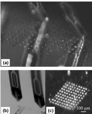
![Figure 1.19: Dip-pen lithography, principle of operation and fabricated patterns [98]](https://thumb-eu.123doks.com/thumbv2/123doknet/2344006.34453/46.892.167.713.476.660/figure-dip-pen-lithography-principle-operation-fabricated-patterns.webp)
![Figure 1.24: Nanofountain probe (NFP) [135]. (a), (b) Writing mechanism of the NFP device](https://thumb-eu.123doks.com/thumbv2/123doknet/2344006.34453/50.892.288.607.125.458/figure-nanofountain-probe-nfp-writing-mechanism-nfp-device.webp)