HAL Id: hal-03039054
https://hal.archives-ouvertes.fr/hal-03039054
Submitted on 3 Dec 2020
HAL is a multi-disciplinary open access
archive for the deposit and dissemination of
sci-entific research documents, whether they are
pub-lished or not. The documents may come from
teaching and research institutions in France or
abroad, or from public or private research centers.
L’archive ouverte pluridisciplinaire HAL, est
destinée au dépôt et à la diffusion de documents
scientifiques de niveau recherche, publiés ou non,
émanant des établissements d’enseignement et de
recherche français ou étrangers, des laboratoires
publics ou privés.
Layered Quaternary Compounds in the Cu 2 S–In 2 S 3
–Ga 2 S 3 system
Maria Caldes, Eric Gau- Tron, Maria Teresa Caldes, Catherine
Guillot-Deudon, Angelica Thomere, Margaux Penicaud, Eric Gautron,
Philippe Boullay, Martine Bujoli-Doeuff, Nicolas Barreau, et al.
To cite this version:
Maria Caldes, Eric Gau- Tron, Maria Teresa Caldes, Catherine Guillot-Deudon, Angelica Thomere,
et al.. Layered Quaternary Compounds in the Cu 2 S–In 2 S 3 –Ga 2 S 3 system. Inorganic
Chem-istry, American Chemical Society, 2020, 59 (7), pp.4546-4553. �10.1021/acs.inorgchem.9b03686�.
�hal-03039054�
1
Layered quaternary compounds in the Cu
2
S-In
2
S
3
-Ga
2
S
3
system
Maria Teresa Caldes*, Catherine Guillot-Deudon*, Angelica Thomere, Margaux Penicaud, Eric
Gau-tron, Philippe Boullay†, Martine Bujoli-Doeuff, Nicolas Barreau, Stéphane Jobic, Alain Lafond
Institut des Matériaux Jean Rouxel – Université de Nantes, CNRS, 2 rue de la Houssinière, BP 32229, 44322 Nantes Cedex 3, France†CRISMAT, CNRS, Normandie University, ENSICAEN, UNICAEN, 14000 Caen, France
ABSTRACT: Several new materials, Cu0.32In1.74Ga0.84S4 (CIGS4), Cu0.65In1.75Ga1.4S5 (CIGS5), Cu1.44In2.77Ga0.76S6 (CIGS6) and
Cu1.1In2.49Ga1.8S7 (CIGS7) have been evidenced in the Cu2S-In2S3-Ga2S3 pseudo ternary system. All of them present a 2D
struc-ture built upon infinite 2/∞[InS2] layers ((InS6) octahedra sharing edges) on which condense on both side mono-, bi-, or tri-
2/∞[MS] layers ((MS4) tetrahedra (M = Cu, In, Ga) sharing corners). (M(Td))n-2(In(Oh))Sn slabs are separated from each
other by a van der Waals gap and subscript n refers to the number of sulfur layers within the building block. These com-pounds have the propensity to display stacking faults but also polymorphic forms. Their optical gap (ca. 1.7 eV) is quite similar to the one of the Cu(In0.7Ga0.3)S2 chalcopyrite absorbers used in tandem solar cells, and the major charge carriers
are holes. This suggests that they might be very attractive for photovoltaic applications in thin film devices but also for photocatalysis.
KEYWORDS : layered CIGS sulfides, crystal structure, electron crystallography, HAADF-imaging, XPS, photovoltaics.
1.Introduction
Among the different photovoltaic technologies, thin film solar cells using a chalcogenide as absorber still awakens interest. Namely, in that context, the quaternary Cu(In,Ga)Se2 (CIGSe)
p-type semiconductor has been extensively studied. Beyond its ability to absorb impinging light and the right position in energy of its valence and conduction bands, one major ad-vantage of this material resides in the ability of its chalcopyrite structure to accommodate a large off-stoichiometry. This makes possible to adjust the chemical composition to desired physical characteristics. In the specific case of CIGSe, it is very well know that a copper deficient (Cu-poor CIGSe) could play a key role for optimizing performances of the cells [1].
Nowa-days, the homologous sulfide compound received much less attention even if investigations have been carrying out for po-tential applications in tandem solar cells.
Therefore, we studied the Cu1-z (In1-xGax)1 + z/3S2 series (Cu-poor
CIGS) and an extended pseudo ternary phase diagram Cu2
S-In2S3-Ga2S3 for the compositions 0.2 ≤ x ≤ 1 and 0 ≤ z ≤ 0.6
could be established [2]. Noticeably, it was clearly
demon-strated that the chalcopyrite structure is much less tolerant towards the copper deficiency in sulfides than in selenides, probably in relation with a lesser covalent character of the cat-ion-anion bonding. A small copper deficiency (z > 0.1) is enough to induce a total collapse of the 3D atomic packing of
the chalcopyrite edifice in CIGS, while such a collapse has never been evidenced in CIGSe. This deviation to the ideal stoichiometry triggers the formation of quaternary CIGS lay-ered compounds.
Since copper deficient phases play a determining role on the performance of solar cells, it seemed important to prepare these new compounds as single phases in order to evaluate their optoelectronic properties before their possible deposi-tion as thin films for solar cells.
In this work, four new layered quaternary compounds in Cu2
S-In2S3-Ga2S3 system have then been identified by combining
single-crystal X-ray diffraction, electron diffraction and chem-ical analysis by EDX. Three of them were successfully prepared as single-phases. Their optical band gaps were then evaluated by diffuse reflectance and the relative valence band maximum (VBM) positioning was determined by XPS.
2. Experimental Section 2.1 Synthesis
Single crystals were issued from three members of the Cu 1-z(In1-xGax)1+z/3S2 series: Cu0.4(In0.5Ga0.5)1.2S2 (z=0.6, x=0.5),
Cu0.4(In0.7Ga0.3)1.2S2 (z=0.6, x=0.3) and Cu0.7(In0.7Ga03)1.1S2
(z=0.3, x=0.3). These compounds were prepared by solid state reactions at high temperature from elemental precursors (Cu,
2
Alfa Aesar 99.9%; In, In corp. of America 6N, Ga, Alfa Aesar-pellet 6mm diam. 6N and S, Aldrich, 99.998%) weighted in stoichiometric ratios. After grinding, the mixture was heated at 100°C/h in a quartz ampoule sealed in vacuum up to 850°C for 96h or 170h or more depending on the samples, and then cooled down to room temperature either by quenching or by cooling at 100°C/h. One or more annealing in the same condi-tions were sometimes required to homogenize the materials. Sulfurization synthesis under H2S was occasionally used. A
mixture of CuO (Aldrich, 99.99%), In2O3 (Alfa Aesar,
99.995%) and Ga2O3 (Alfa Aesar, 99.999%) was heated at
900°C during 3h. A posterior heat treatment at 850°C for 170h was done in a quartz ampoule sealed in vacuum. The synthesis conditions for each of the targeted compositions prepared are summarized in Table S1.
Thin films were prepared by the coevaporation of the ele-ments in high vacuum from effusion cells (copper, indium, gallium and sulfur) using so-called one-step process. After the deposition, the thin films were dipped in a KCN solution (0.1M for 5 min) to remove CuxSy from the surface. The average
com-position was determined by EDX analysis. 2.2 Chemical analyses
The chemical compositions of the prepared samples were an-alyzed using an EDX-equipped scanning electron microscope (JEOL 5800LV) on polished sections of the products embed-ded in epoxy. The elemental percentages were calculated us-ing calibrated internal standards under the followus-ing operat-ing conditions: acceleratoperat-ing voltage 20 kV, standards Cu (Cu Kα), In (InAs Lα), Ga (GaP K) and S (FeS2 Kα). This technique
allowed us also to check the chemical homogeneity of sam-ples.
2.3 Powder X-ray diffraction
The powder X-ray diffraction (PXRD) experiments were per-formed with the use of a Bruker D8 Advance diffractometer (Bragg Brentano, θ/2θ geometry, CuK-L3, λ = 1.540598 Å) equipped with a LynxEye detector. All the powder patterns were recorded in the 4°- 100° 2θ- range with a 2θ-step of 0.011°. Le Bail and Rietveld analyses were carried out with the help of the program JANA2006 [3].
2.4 Single crystal X-ray diffraction.
Suitable single crystals were picked up in each of powdered samples. The studied crystals were often of poor quality be-cause of their lamellar feature (see below). The data collec-tions were carried out at ambient temperature on a Bruker-Nonius Kappa CCD diffractometer using graphite monochro-matic MoKα. Data integration was processed with the set of programs from Nonius using the Eval CCD formalism. The crystal shape and size optimization for absorption were per-formed with the X-Shape program while refinements were carried out with the JANA2006 program.
2.5 Transmission electron microscopy
High-angle annular dark-field imaging (HAADF) was per-formed with a probe corrected scanning transmission electron microscope (S/TEM) Themis-Z (Thermo Fisher Scientific) with these experimental conditions: 300 kV accelerating volt-age, 21 mrad convergence angle, 63-200 mrad collection angle. The compounds were gently ground in ethanol before being deposited on a holed carbon film supported by a copper grid
for examination. Precession electron diffraction tomography (PEDT), was performed with a Jeol 2010 electron microscope (operating at 200 kV with a LaB6 cathode) equipped with a Nanomegas DigiStar precession module and an upper-mounted Gatan ORIUS 200D CCD camera. PEDT data sets of nonoriented patterns were recorded on several different thin crystals. For data collections the precession angle was set to 1.6° with a goniometer tilt step 1°. PEDT data sets were ana-lyzed using the computer programs PETS [4] and JANA2006.
2.6 X-ray photoelectron spectroscopy
X-ray photoelectron spectroscopy (XPS) measurements were performed on a Kratos axis Nova spectrometer (monochro-matic Al Kα X-ray source, 1486.6 eV). Studies were carried out on pellets mounted on double-sided carbon tape on an alu-mina plate. An electron flood gun was used to elialu-minate any surface charging effect. The pass energy was 160 eV for wide scan spectra and 40 eV for narrow scan and the valence band (VB) region (instrumental resolution of 0.1 eV). Spectra were calibrated using the C 1s peak at 284.8 eV. All high-resolution spectra were analyzed and fitted with the CasaXPS software [5]. The valence band maximum (VBM) position was
deter-mined for all probed samples by linearly extrapolating the low binding energy (BE) edge of the VB region
2.7 Diffuse reflectance measurements
The ultraviolet−visible light−near-infrared (UV-vis-NIR) dif-fuse reflectance spectra of finely ground samples were rec-orded with a UV/vis/NIR spectrometer (PerkinElmer Lambda 1050) equipped with an integration sphere. The UV Winlab 6 program was used to control experiments. The reflectance measurements were made in the 850−400 nm range (i.e. 1.46 eV- 3.10 eV) at a resolution of 2 nm. A barium carbonate blank was used to normalize the measured reflectance. The absorp-tion (K/S) data were then calculated from the raw reflectance using the K/S = (1 R)2/(2R) Kubelka-Munk function [6]. The
optical gap value was determined for all probed samples by linearly extrapolating.
3. Results and discussion
As already mentioned by Thomere et al., attempts to synthe-size Cu1-z(In1-xGax)1 + z/3S2 compounds [2] systematically leads
to multiphasic samples for z> 0.1 (see pseudo-ternary diagram shown in Figure 1). Typical PXRD patterns corresponding to nominal compositions Cu0.7(In0.7Ga03)1.1S2 (z=0.3, x=0.3),
Cu0.4(In0.7Ga0.3)1.2S2 (z=0.6, x=0.3) and Cu0.4(In0.5Ga0.5)1.2S2
(z=0.6, x=0.5) are shown in Figure S 1. Corresponding targets are imaged in Figure 1.
3
Figure 1. Pseudo-ternary diagram of the Cu2S-In2S3-Ga2S3
sys-tem. x refers to the Ga/(Ga+In) ratio, and z to the copper de-ficiencies relative to the Cu(In,Ga)S2 composition The hashed
zone corresponds to a multiphasic domain. Following tar-geted compositions are imaged as blue symbols: Cu0.4(In0.5Ga0.5)1.2S2 (square), Cu0.4(In0.7Ga0.3)1.2S2 (triangle) and
Cu0.7(In0.7Ga03)1.1S2 (circle)
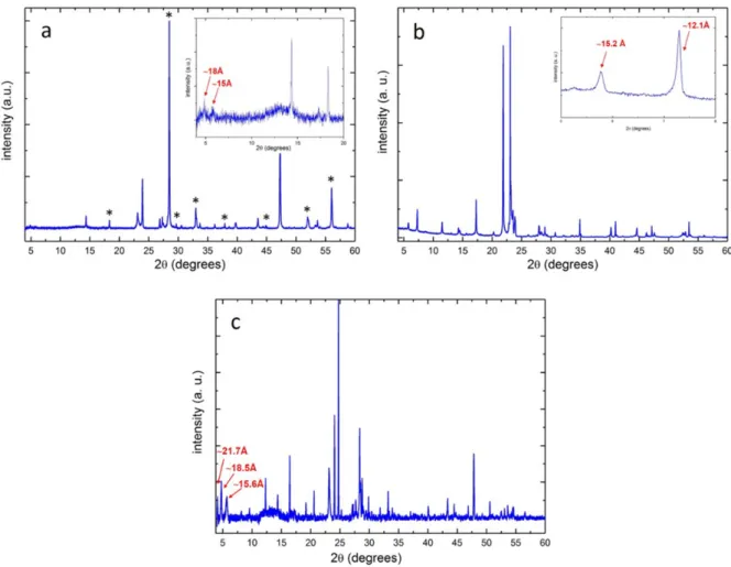
As inferred from the d-spacing values observed at low two-theta angles (i.e. 12 Å, 15.7 Å, 18.7 Å and 21.7 Å), several new quaternary phases, very Cu-poor compared to Cu(In1-xGax)S2
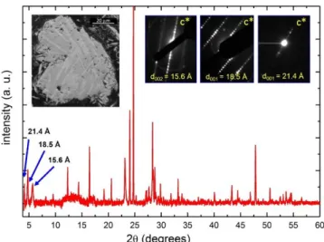
chalcopyrite (SG I 4�2d, a∼5.47 Å, c∼10.96 Å), were identified (see Table 1). This fact was exemplified in Figure 2 where three of the four phases identified, were detected by combining XRD, electron diffraction and backscattered electron imaging analysis. Each of the first three reflections observed in the DRX pattern, corresponds respectively to the inter-reticular distance d (001) of each new phase. The fourth one has been detected in the targeted composition Cu0.4(In0.7Ga0.3)1.2S2 (see
Figure S1).
Figure 2. XRD pattern of Cu0.4(In0.5Ga0.5)1.2S2 multiphasic
com-pound. ED patterns corresponding to three different phases are shown at top right of the image. In the top left, the SEM backscattered electron image evidences the coexistence sev-eral phases.
Some of these d-spacing have already been described for some layered compounds in the Ga2S3-In2S3 system: GaInS3 (c=18.2
Å) [7], Ga0,75In1,25S4 (c=12.23 Å) [8], Ga1,74In2,92S7 (c=21.14 Å) [9].
However, they have never been reported before for quaternary compounds in the pseudo-ternary diagram Cu2S-In2S3-Ga2S3.
Moreover, the structural models proposed for Ga0,75In1,25S4
(c=12.23 Å) and Ga1,74In2,92S7 (c=21.14 Å) do not respect the
cri-teria of charges neutrality:
In Table 1 the multiphase feature of three targeted composi-tions is illustrated. Four different Cu/S ratios are thus identi-fied: one corresponding to the chalcopyrite structure (Cu/S = 0.49) and three others corresponding to new quaternary Cu-poor phases. The In/S and Ga/S ratios can be different for the same Cu/S ratio.”
Table 1. EDX atomic ratios of quaternary phases detected in each multiphasic sample. The different colors figure out dis-similar Cu/S ratios.
Targeted
composition Cu/S In/S Ga/S Cu0.4(In0.5Ga0.5)1.2S2 phase 1 0.27(3) 0.14(2) 0.50(3) phase 2 0.19(2) 0.28(3) 0.39(3) phase 3 0.18(2) 0.34(3) 0.30(3) Cu0.7(In0.7Ga0.3)1.1S2 chalco-pyrite 0.49(3) 0.30(3) 0.23(2) phase 2 0.27(3) 0.43(3) 0.16(2) Cu0.4(In0.7Ga0.3)1.2S2 phase 1 0.19(2) 0.43(3) 0.19(2) phase 2 0.08(2) 0.44(3) 0.23(2)
To solve the structure of these new quaternary compounds, four suitable crystals were picked up in the three aforemen-tioned powdered samples. Their chemical composition was obtained by EDX analyses.
Clearly, four types of layered compounds were identified. They were named CIGS4 (Cu0.32In1.74Ga0.84S4), CIGS5
(Cu0.65In1.75Ga1.4S5), CIGS6 (Cu1.44In2.77Ga0.76S6) and CIGS7
(Cu1.1In2.49Ga1.8S7), according to both chemical composition
and number of anionic layers in the structure (i.e. Sn).
The structures of CIGS4-CGS7 are depicted in Figure 3. All
ex-hibit a marked 2D character with 2/∞[InS2] layers built upon
(InS6) octahedra sharing edges (CdI-like slabs) on which
dense on both side mono-, bi-, or tri- 2/∞[MS] layers that con-sist of (MS4) tetrahedra (M = Cu, In, Ga) sharing corner. This
leads to (M(Td))n-2(In(Oh))Sn slabs separated to each other by a
van der Waals gap of about 3.75 Å. CIGSn phases are
conse-quently characterized by specific d-spacing, ca. 12.2, 15.7, 18.7 and 21.7 Å for CIGS4, CIGS5, CIGS6 and CIGS7, related to their
slabs thickness. Let us notice that n can be even or odd. In the latter case, this implies that the number of MS layers above a 2/∞[InS2] layer is different from the number of MS layers
be-low (and vice versa) with distribution of Cu, In and Ga atoms on Td sites possibly distinct above and below.
4
Figure 3. Structure models of CIGS4 (Cu0.32In1.74Ga0.84S4), CIGS5
(Cu0.65In1.75Ga1.4S5), CIGS6 (Cu1.44In2.77Ga0.76S6) and CIGS7
(Cu1.1In2.49Ga1.8S7).
Refinement results for all compounds are given in Table 2. All the structures were refined in P63mc space group or its sub-group P-3m1. Atomic positions and atomic displacements pa-rameters (ADP) are shown in Tables S2-S5.
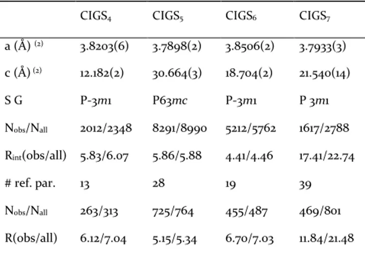
Table 2. Main crystal data and structure refinement results for CIGSn phases
CIGS4 CIGS5 CIGS6 CIGS7
a (Å) (2) 3.8203(6) 3.7898(2) 3.8506(2) 3.7933(3) c (Å) (2) 12.182(2) 30.664(3) 18.704(2) 21.540(14) S G P-3m1 P63mc P-3m1 P 3m1 Nobs/Nall 2012/2348 8291/8990 5212/5762 1617/2788 Rint(obs/all) 5.83/6.07 5.86/5.88 4.41/4.46 17.41/22.74 # ref. par. 13 28 19 39 Nobs/Nall 263/313 725/764 455/487 469/801 R(obs/all) 6.12/7.04 5.15/5.34 6.70/7.03 11.84/21.48 Rw(obs/all) 21.38/21.60 14.48/14.56 22.34/22.43 19.01/22.31 ρ (e-/Å3)+/- 6.38/-3.08 3.32/-2.69 5.21/-3.73 10.58/-7.33
For all crystals, the octahedral sites (Oh) are exclusively and fully occupied by indium atoms. In contrast, tetrahedral sites (Td) can be partially vacant and a mixed occupancy is often observed. Because Cu+ and Ga3+ cations are isoelectronic and
not distinguishable by conventional X-ray diffraction, the oc-cupation of mixed Td sites was determined by considering simultaneously various criteria, namely the chemical compo-sition of the single crystals revealed by EDX, the evolution of the ADPs during the refinement, and the value of the cation-sulfur distances refined for each type of site. Interatomic dis-tances for the four refined compounds CIGS4, CIGS5, CIGS6
CIGS7. are gathered in Table S6. They all match with those
re-ported in the literature for other phases with similar chemical environments [10–12]. As expected, the In-S bond distances in a
octahedral site (2.6 Å, 𝑟𝑟𝐼𝐼𝐼𝐼3+(𝑂𝑂ℎ) = 0.80 Å) are larger than the
In-S bonds in tetrahedral environment (∼2.4 Å, 𝑟𝑟𝐼𝐼𝐼𝐼3+(𝑇𝑇𝑇𝑇) = 0.60
Å) that are larger than Cu(Ga)-S ones (∼2.3 Å, 𝑟𝑟𝐶𝐶𝐶𝐶+(𝑇𝑇𝑇𝑇) = 0.46
Å, 𝑟𝑟𝐺𝐺𝐺𝐺3+(𝑇𝑇𝑇𝑇) = 0.47 Å). However, the presence of vacancies leads
systematically to a slight shortening of cation-sulfur bond dis-tances compared to the expected ones. In these lamellar com-pounds, the vacancy rate of Td sites never exceeds 20% except for CIGS7 in which a mixed site (In-Cu) exhibits a vacancy rate
of 50%. It is also worth noticing that indium atoms in tetrahe-dral sites are preferentially located at the van de Waals gap frontier, probably for steric reasons
Indeed, CIGS4 with a sequence Td(Cu,In,Ga, )-Oh(In)-Td(Cu,In,Ga, )
sequence, CIGS5 (Td(In,Ga)-Td(Cu,Ga, )-Oh(In)-Td(Cu,In)) and CIGS6
(Td(Cu,Ga)-Td(Ga,In, )-Oh(In)-Td(Cu,Ga)-Td(Ga,In, )) are isostructural
to ZnIn2S4-type I, Zn2In2S5-type IIa and Zn3In2S6, respectively
[13]. The CIGS5 stacking type has been also already observed
for Ag1.25Ga2.5In3.75S10 [14]. Conversely CIGS7 (Td(In,Ga)-Td(Cu,In, )
-Td(Ga, )-Oh(In)-Td(In,Ga)-Td(Cu)) exhibits an unprecedented
lay-ered stacking. At this stage, let us also mention that GaInS3 [7],
Ga0.75In1.25S4 (c=12.23 Å) [8], Ga1.74In2.92S7 (c=21.14 Å) [9] are
probably also members of the aforementioned series (n= 6, n= 4 and n=7, respectively) but for two last compounds, a chem-ical element is obviously missing to respect the charge bal-ance.
Although we have been able to elucidate the structure of these four quaternary phases using X-ray single crystal diffraction, it is worth noting that the Rw remain high for all the structures
and Fourier difference maps show large residuals along c axis. The high values of Rw are partially due to the difficulty to
de-scribe accurately the occupation of Td sites, since the intensity of several strong reflections highly depends on it. On the other hand, the faulted feature of the crystals can also lead to large errors. Due to the strong structural similarity in between (M(Td))n-2In(Oh) Sn blocks and the 2D character of these
build-ing entities, intergrowths, stackbuild-ing faults and turbostratic dis-order could exist that may explain difficulties met to properly refine structures. In fact, the quality of the single crystals was often poor. To illustrate this purpose, the experimental (h0l) * reciprocal plane corresponding to the single crystal of CIGS4
is shown in figure S2. The extra reflections observed along the c* axis, could be attributed to the stack of several platelets (see
5
inserted image) but probably also to the existence of stacking faults. Although these extra reflections are not considered during integration process, their presence could induce an er-ror during intensities measurement. For all these reasons, the structure models of CIGSn should probably be considered as
average structures.
In Figure 4, the [100] electron diffraction pattern of a faulted crystal and its corresponding TEM image are shown. The streaking of diffraction spots observed along c*-axis testify of a strong structural disorder. Actually, the Z-contrast image (HAADF-STEM) figures out intergrowths. In this type of im-ages, the brightness level is proportional to the averaged atomic number of the projected atomic columns observed. Ac-cordingly, the 2/∞ [InS2] octahedral layers appear as brighter
spots rows and tetrahedral (MS4) ones like gray rows. The Van
der Waals gap is imaged as a dark area. The number of tetra-hedral layers on each side of the 2/∞ [InS2] layers can be then
easily counted and the different members of the series (M(Td))n-2(In(Oh))Sn can thus be identified (see annotations in
Figure 4 and Figure S2 for a large field of view).
Figure 4. [100] electron diffraction pattern, corresponding TEM image and HAADF-STEM image (on the bottom) of a faulted crystal, highlighting the propensity of CIGSn materials
to contain intergrowth defects (the value n from (M(Td)) n-2(In(Oh))Sn is given for each slab). The van der Waals gaps are
imaged as dark contrast lines.
Therefore, we decided to reduce the size of the probe, in order to find nanocrystals much better organized than those used for SCXRD. Thus, we investigated the structure of CIGSn
phases using PEDT. Faulted crystals were also evidenced irre-spective of their size. Nonetheless, it was possible to solve the 2Td-Oh-2Td layer stacking of CIGS6 and refined it [15] to a final
model consistent with that obtained by SCXRD. Taking into account the charge balance equilibrium and thermal displace-ment parameters, the final refinedisplace-ment led to the following chemical formula Cu1.2In2.54Ga1.06S6. Refinements results are
summarized in Tables S7-S8. The chemical composition of the crystal studied by PEDT is significantly different from that of one studied by SCDRX (Cu1.44In2.77Ga0.76S6). This feature is
possible due to the great occupation flexibility (Cu, Ga, In) ex-hibited by Td-sites in these lamellar structures. Indeed, for a given CIGSn structure-type, different chemical compositions
may exist.
To try to obtain CIGSn compounds as powdered single-phase
samples, prior synthesis conditions were modified Instead of using elements as reactants, gallium, indium and copper sul-phides were used. On the other hand, the reaction time was reduced from 170 to 48 hours and samples were quenched. Chemical compositions of single crystals studied were used as target. Figure S3 and Figure 5 display the PXRD patterns of as-prepared CIGS4, CIGS5 and CIGS6 compounds (attempts to
prepare CIGS7 as powder without sub-products in large
amount never succeeded).
Figure 5. XRD pattern and Le Bail refinement of CIGS5
com-pound
For all compounds, Le Bail refinements attest that most of the observed reflections can be indexed considering unit cells pa-rameters and space groups obtained by SCXRD. However, in the case CIGS4 and CIGS6 (see Figure S2 in S.I), extra phases
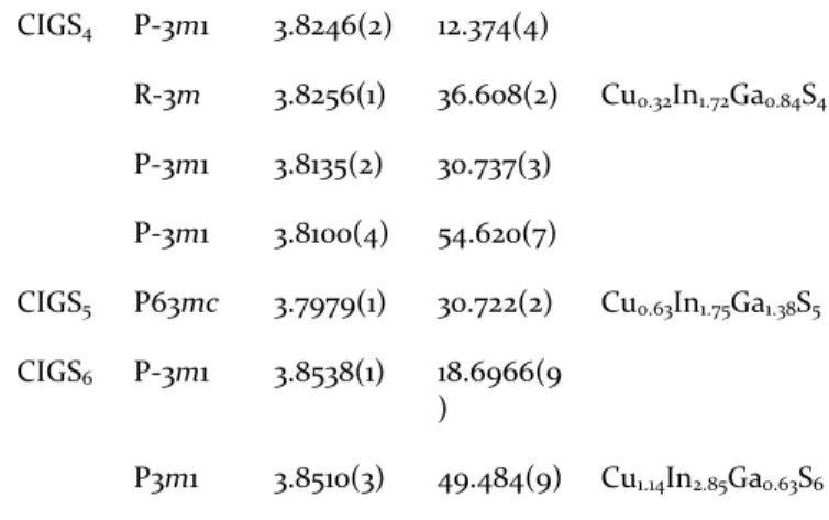
had to be considered to explain all reflections. Indeed, these secondary phases can be considered as polytypes since EDX analyses confirm a single chemical composition and electron diffraction attest to the existence of at least two kinds of crys-tals. Refined cell parameters and EDX results are all summa-rized in Table 3. Four polytypes have been identified for CIGS4
and two for CIGS6.
Table 3. Cell parameters of CIGS4, CIGS5 and CIGS6 issued
from a Le Bail refinement of the collected XRD pattern and chemical compositions issued from a EDX analysis.
6
CIGS4 P-3m1 3.8246(2) 12.374(4) R-3m 3.8256(1) 36.608(2) Cu0.32In1.72Ga0.84S4 P-3m1 3.8135(2) 30.737(3) P-3m1 3.8100(4) 54.620(7) CIGS5 P63mc 3.7979(1) 30.722(2) Cu0.63In1.75Ga1.38S5 CIGS6 P-3m1 3.8538(1) 18.6966(9 ) P3m1 3.8510(3) 49.484(9) Cu1.14In2.85Ga0.63S6The existence of polytypes for the different members of the ((Cu,In,Ga)(Td))n-2(In(Oh))Sn series is not surprising as
exempli-fied for ZnIn2S4 that exhibits at least four polymorphs (i.e.
ZnIn2S4 (I), ZnIn2S4(IIa), ZnIn2S4(IIb) and ZnIn2S4(IIIa)) that
differs in the long rang ordering of the Td-Oh-Td blocks along the stacking axis and/or distribution of cations within Td sites. In fact, this propensity for polymorphism is observed for dif-ferent members of the ZnmIn2S3+m series as discussed by H.
Haeuseler et al [12]
Attempts to separate the two polymorphic forms of CGIS4 and
CIGS6 via sulfurization of oxides was initiated and turn out to
be successful for the latter. Indeed, as shown in Figure 6, the
majority of experimental reflections observed in the PXRD could be indexed successfully by considering a single poly-morph (SG P-3m1 a=3.86, c= 18.69 Å).
Figure 6. XRD pattern and Le Bail refinement of monophasic-CIGS6 compound Broad reflections (*) are slab intergrowths fingerprint.
Clearly, the driving force to the formation of lamellar CIGSn
phases lies in the preference of In3+ cations for an octahedral
environment in sulfides (even if In3+ cations can also be
tetra-coordinated), while Cu+ and Ga3+ cations favor tetrahedral
sites. Thus, all indium-free CGS ternary compounds existing in the CuGaS2-Ga2S3 composition line (see Figure 1), exhibit
structure types built upon the packing of [MS4] tetrahedra (i.e.
chalcopyrite, stannite, or defect sphalerite). Tetrahedral coor-dination is always preferred independently the copper rate in the compound. In contrast, for gallium-free CIS compounds (CuInS2-In2S3 line, a tiny copper vacancies rate is enough to
destabilize the chalcopyrite structure of CuInS2 (2Td sites)
be-cause the difference in site preference between copper and in-dium atoms. Thus, several compounds (i.e. CuIn5S8) with a
spinel structure containing a majority of octahedral sites (1Td, 2 Oh) are formed.
The behavior of the CIGS quaternary compounds described in the composition zone Cu1-zGa1+z/3S2- Cu1-zIn1+z/3S2 (see Figure 1)
is intermediate between that of thiogallates CGS and thioin-dates CIS, given the coexistence of gallium and indium in these compounds. As in the case of thioindates, copper vacan-cies rapidly destabilize the chalocopyrite structure and thus the tetrahedral environment of indium atoms. However, the presence of gallium seems to guide the structural evolution towards lamellar structures, in which the Td and Oh environ-ments coexist even if, contrary to the spinel structure, tetra-hedral coordination remains predominant: CIGS4 (2Td, 1Oh),
CIGS5 (3Td, 1Oh), CIGS6 (4Td, 1Oh) et CIGS7 (5Td, 1Oh).
The flexibility of stoichiometric CIGS compounds to accept copper deficiencies as well as the identification of lamellar CIGS phases could be a key point to better understand struc-tural phenomena described in the literature for CIGS-based solar cells. As a matter of fact, an angular step (26° ≤ 2θ ≤ 28°) with asymmetric profile is observed in the PXRD patterns of Cu-poor CIGS thin films. This feature has been related to stacking faults occurrence in the bulk [16,17]. In Figure 7, the
PXDR patterns of two CIGS thin films prepared by coevapora-tion, with experimental compositions Cu0.89In0.76Ga0.24S2
(Cu-poor) and CuIn0.7Ga0.3S2 (Cu-stoichiometric) are compared to
those of CIGS5 and CIGS6 compounds. As observed, some
main reflections of lamellar compounds match fairly well with the broad angular step observed into the Cu-poor thin film pattern. This prompt us to wonder whether the stacking faults reported in the literature could actually correspond to the sta-bilization of the Cu-poor lamellar compounds. Actually, to de-posit the CIGS absorber of a thin film solar cell, a multi-steps process is used including a Cu-poor stage. This last could fa-cilitate the formation of lamellar compounds as secondary phases embedded into the chalcopyrite bulk. It is therefore important, to evaluate whether the optoelectronic properties of the lamellar CIGSn phases are very different from those of
7
Figure 7. Comparison in the 25-39° 2θ-range of PXDR patterns of two CIGS thin films with experimental compositions Cu-poor Cu0.89In0.76Ga0.24S2 (black) and Cu-stoichiometric
CuIn0.7Ga0.3S2 (red). In the insert, the diagrams of CIGS5 and
CIGS6 compounds are superimposed on broad angular step
observed into the Cu-poor thin film pattern around the (112) reflection.
Optoelectronic properties of the lamellar CIGSn phases were
analyzed by diffuse reflectance and X-ray photoelectron spec-troscopies.
The Kubelka-Munk transformed diffuse reflectance spectra of CIGS4,CIGS5 and CIGS6 prepared by sulfurization are shown
in Figure 8. The spectrum of the stoichiometric CuIn0.7Ga0.3S2
CIGS chalcopyrite compound is given for comparison. As in-ferred from Table 4, the optical gaps of four compounds are the same order of magnitude, however Eg slightly increases with copper content decreasing. Thus, chalcopyrite CuIn0.7Ga0.3S2 with a Cu/S ratio equal to 0.5, exhibits an Eg ∼
1.6 eV while that of CIGS4 compound (Cu/S = 0.08) is equal to
1.9 eV. It should be noted that the Eg measured for CIGS4,
should correspond to an average of those of two polymorphs coexisting These results suggest that these lamellar phases could be potential substitutes to Cu-poor CIGS chalcopyrite phases for tandem solar cell applications.
Figure 8. Kubelka-Munk transformed reflectance spectra of CIGS4, CIGS5, CIGS6 and CuIn0.7Ga0.3S2 chalcopyrite.
Table 4. Optical gaps and position of the uppermost level of the valence band vs. Fermi level
Cu/S Eg (eV) VBM /EF*
CIGS4 0.08 1.9 1.0
CIGS5 0.13 1.8 0.6
CIGS6 0.2 1.6 0.9
CIGS7 0.5 1.6 0.8
*The binding energy is referred to the EF at BE=0 eV
XPS measurements were initiated to get insight on the nature of charge carriers and the positioning of the uppermost levels of the valence band. Spectra in the 0-10 eV binding energy range are plotted in Figure 9. The striking feature concerns the spectrum shape in the 0.5-6 eV domain, quite different for chalcopyrite and lamellar compounds. The former exhibits two well defined separated peaks the latter a unique broad band. At very first sight, based on the calculated electronic structures of GaInS3 [18] the band peaking at ca. 4 eV might be
associated with copper 3d orbitals hybridized with 3p orbitals of sulfur atoms, while the one at ca. 8 eV, much less intense, to Ga and In orbitals mixed with S.
Figure 9. XPS valence band spectra of CIGSn series and
CuIn0.7Ga0.3S2 compound in [-10-0] eV range.
For the four investigated materials, the binding energy thresh-old is in the 0.5-1 eV range (Table 4). This suggests that CIGS4,
More-8
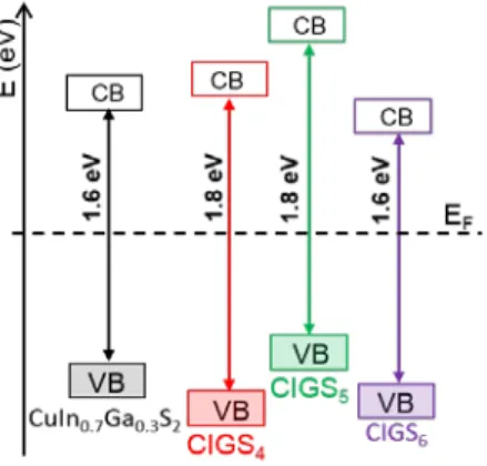
over, based on XPS and reflectance (absorption) measure-ments, the relative positions of valence and conduction bands of CIGSn compounds can be determined. An energy diagram
is sketched in Figure 10. A slight change in the VB and CB po-sitioning is noted. It may impact the electronic flow in a solar cell device and these materials would deserve to be tested as absorber.
Figure 10. Sketch of the energy diagrams of probed materials
4.Concluding remarks
We reported here on the existence of several new lamellar CIGSn compounds in the Cu2S/In2S3/Ga2S3 system. These
ma-terials built upon cations in 4-fold and 6-fold coordination of sulfur, exhibit a marked 2D character with a van der Waals gap what singularly contrasts with the 3D chalcopyrite Cu(In,Ga)S2 materials with a dense structure consisting of
only tetrahedra sharing edges. The aforementioned phases are very new members of the (M(Td))n-2In(Oh)Sn series that could
be declined with In3+ cations in Oh environment and Mm+
cat-ions in Td environment. Mm+ is a trivalent cation or a mixture
of mono-, di- or trivalent cations, vacancies at the Td sites be-ing possibly present to ensure the charge balance. Let us no-tice that In3+ cations in Oh site could be substituted for many
other trivalent cations with a pronounced preference for the 6-fold coordination. Due the multiple possibilities to dispatch cations over tetrahedral sites with possible change in the long range ordering without modification of the overall stoichiom-etry, due to the strong similarities between all the building en-tities of the series, these materials are subject to stacking faults but also polytypisms and chemical composition deviations that open an avenue for the stabilization of new materials. Therefore, we are currently studying composition ranges for each CIGSn compound, by preserving their characteristic Cu/S
and Cu/In(Oh) ratios but varying the Ga(Td)/In(Td) one.
Surprisingly, optical gaps of CIGS4, CIGS5 and CIGS6
com-pounds are comparable to the one of Cu(In0.7Ga0.3)S2 material
currently investigated for potential use as absorber in tandem solar cell. This suggests this new series of materials may also present interesting characteristics for photovoltaic applica-tions. Investigations are currently in progress to deposit them as thin films. Moreover, the very large range of possible com-positions with multiples possible defects opens up the door to compounds with defect (intermediate) levels in the gap that can be benefit for photovoltaics but also for photocatalysis.
These phases are currently explored to deepen our knowledge in these domains.
ASSOCIATED CONTENT
Supporting Information. (1) Typical PXRD patterns
corre-sponding to nominal compositions Cu0.7(In0.7Ga03)1.1S2 (z=0.3,
x=0.3), Cu0.4(In0.7Ga0.3)1.2S2 (z=0.6, x=0.3) and
Cu0.4(In0.5Ga0.5)1.2S2 (z=0.6, x=0.5)., (2-5) Atom coordinates,
ADP and occupancy rate of each atomic sites of CIGS4, CIGS5,
CIGS6, CIGS7 respectively, (6) Interatomic distances for CIGSn
compounds, (7-8) Atom coordinates, ADP and occupancy rate of each atomic sites of CIGS6 from PEDT data, (9) HAADF-STEM image of a faulted crystal, highlighting the propensity of CIGSn materials to contain intergrowth defects (10) PXRD patterns of as-prepared CIGS4 and CIGS6 compounds.
AUTHOR INFORMATION
Corresponding Author
* E-mail: maite.caldes@cnrs-imn.fr, catherine.deudon@cnrs-imn.fr.
AKNOWLEDGEMENTS
The authors acknowledge financial support from the CNRS-CEA “METSA” French network (FR CNRS 3507) on the plate-form IRMA (CRISMAT – Caen).
REFERENCES
(1) Caballero, R.; Kaufmann, C. A.; Efimova, V.; Rissom, T.; Hoffmann, V.; Schock, H. W. Investigation of Cu(In,Ga)Se 2 Thin-Film Formation during the
Multi-Stage Co-Evaporation Process: CIGSe Thin-Film For-mation Multi-Stage Co-Evaporation Process. Prog.
Pho-tovolt. Res. Appl. 2013, 21 (1), 30–46. https://doi.org/10.1002/pip.1233.
(2) Thomere, A.; Guillot-Deudon, C.; Caldes, M. T.; Bodeux, R.; Barreau, N.; Jobic, S.; Lafond, A. Chemical Crystallographic Investigation on Cu2S-In2S3-Ga2S3 Ternary System. Thin Solid Films 2018, 665, 46–50.
https://doi.org/10.1016/j.tsf.2018.09.003.
(3) Petricek V.; Dusek M. and Palatinus L. . The Crystallo-graphic Computing System.
(4) Palatinus, L. PETS-Program for Analysis of Electron
Dif-fraction Data; Institute of Physics of the CAS: Praha
Czechia, 2011.
(5) Neal Fairley. CasaXPS Software Ltd.
(6) Kubelka, P.; Munk, F. An Article on Optics of Paint Lay-ers. Tech Phys 1931, 12, 593–601.
(7) Amiraslanov, I.R; Azizov, T. Kh.; Guseinov, G.G.; Kuliev, A.S.; Niftiev, G.M. Crystal Growth, Structure, and Pho-toelectric Properties of New Polymorph of Gallium In-dium Sulfide (GaInS3). Izv. Akad. Nauk SSSR
Neor-ganicheskie Mater. 1988, 24 (5), 723–726.
(8) Amiraslanov, I.R; Veliyev, R.B.; Misayev, A.A.; Asadov, S.G.; Gyseynov, G.G. On the Phase Formation in Ga2S-In2S3 System and the Crystal Structure of Ga0.5In1.5S3.
Doklady - Akademiya Nauk Azerbaidzhanskoi SSR. 1990,
9
(9) Amiraslanov, I.R; Asadov, F. Yu.; Musaev, A.A.; Guseinov, G.G. Crystal Structure of the New Layered Semiconductor Ga1.74In2.92S7. Kristallografiya 1989,
34 (4), 1012–1013.
(10) Binsma, J. J. M.; Giling, L. J.; Bloem, J. PHASE RELATIONS IN THE SYSTEM Cu2 S—In2S3. J. Cryst.
Growth 1980, 50, 429–436.
(11) Maeda, T.; Yu, Y.; Chen, Q.; Ueda, K.; Wada, T. Crystal-lographic and Optical Properties and Band Diagrams of CuGaS 2 and CuGa 5 S 8 Phases in Cu-Poor Cu 2 S–Ga 2 S 3 Pseudo-Binary System. Jpn. J. Appl. Phys. 2017, 56 (4S),
04CS12. https://doi.org/10.7567/JJAP.56.04CS12. (12) Paorici, C.; Zanotti, L.; Gastaldi, L. Preparation and
Structure of the CuIn5S8 Single-Crystalline Phase.
Ma-ter. Res. Bull. 1979, 14 (4), 469–472. https://doi.org/10.1016/0025-5408(79)90187-9.
(13) Haeuseler, H.; Srivastava, S. K. Phase Equilibria and Layered Phases in the Systems A2X3±±M2X3±±MHX (A = Ga, In; M = Trivalent Metal; MH = Divalent Metal; X = S, Se). 1999, 17.
(14) Ivashchenko, I. A.; Danyliuk, I. V.; Olekseyuk, I. D.; Pankevych, V. Z.; Halyan, V. V. Phase Equilibria in the Quasiternary System Ag2S–Ga2S3–In2S3 and Optical
Properties of (Ga55In45)2S300, (Ga54.59In44.66Er0.75)2S300 Single Crystals. J. Solid
State Chem. 2015, 227, 255–264.
https://doi.org/10.1016/j.jssc.2015.04.006.
(15) Palatinus, L.; Corrêa, C. A.; Steciuk, G.; Jacob, D.; Rous-sel, P.; Boullay, P.; Klementová, M.; Gemmi, M.; Ko-peček, J.; Domeneghetti, M. C.; et al. Structure Refine-ment Using Precession Electron Diffraction Tomogra-phy and Dynamical Diffraction: Tests on Experimental Data. Acta Crystallogr. Sect. B Struct. Sci. Cryst. Eng.
Mater. 2015, 71 (6), 740–751. https://doi.org/10.1107/S2052520615017023.
(16) Guo, Q.; Kim, S. J.; Kar, M.; Shafarman, W. N.; Birkmire, R. W.; Stach, E. A.; Agrawal, R.; Hillhouse, H. W. Devel-opment of CuInSe 2 Nanocrystal and Nanoring Inks for
Low-Cost Solar Cells. Nano Lett. 2008, 8 (9), 2982–2987.
https://doi.org/10.1021/nl802042g.
(17) Rodriguez-Alvarez, H.; Barreau, N.; Kaufmann, C. A.; Weber, A.; Klaus, M.; Painchaud, T.; Schock, H.-W.; Mainz, R. Recrystallization of Cu(In,Ga)Se2 Thin Films Studied by X-Ray Diffraction. Acta Mater. 2013, 61 (12),
4347–4353. https://doi.org/10.1016/j.ac-tamat.2013.04.006.
(18) Khyzhun, O. Y.; Halyan, V. V.; Danyliuk, I. V.; Ivash-chenko, I. A. Electronic Structure of (Ga55In45)2S300 and (Ga54.59In44.66Er0.75)2S300 Single Crystals. J.
Mater. Sci. Mater. Electron. 2016, 27 (4), 3258–3264.
10
Several new layered materials, CIGSn have been evidenced in
the Cu2S-In2S3-Ga2S3 system. (M(Td))n-2(In(Oh))Sn slabs are
separated from each other by a van der Waals gap and sub-script n refers to the number of sulfur layers within the build-ing block. Their optical gap is quite similar to the one of the Cu(In0.7Ga0.3)S2 chalcopyrite absorbers used in tandem solar
cells. They might be very attractive for photovoltaic applica-tions in thin film devices but also for photocatalysis.
S1
Supporting Information for “New layered quaternary
compounds in the Cu
2
S-In
2
S
3
-Ga
2
S
3
system”
M.T. Caldes*, C. Guillot-Deudon*, A. Thomere, M. Penicaud, Eric Gautron, P. Boullay†, M. Bujoli-Doeuff, Nicolas Barreau, S.Jobic, A. Lafond
Institut des Matériaux Jean Rouxel – Université de Nantes, CNRS, 2 rue de la Houssinière, BP 32229, 44322 Nantes Cedex 3, France
†CRISMAT, CNRS, Normandie University, ENSICAEN, UNICAEN, 14000 Caen, France Corresponding Authors
* E-mail: maite.caldes@cnrs-imn.fr, catherine.deudon@cnrs-imn.fr.
Figure S1: Typical PXRD patterns corresponding to nominal compositions: (a) Cu0.7(In0.7Ga03)1.1S2 (z=0.3,
x=0.3), (b) Cu0.4(In0.7Ga0.3)1.2S2 (z=0.6, x=0.3) and (c) Cu0.4(In0.5Ga0.5)1.2S2 (z=0.6, x=0.5). In Figure S1a, the
S2
Table S1. Synthesis conditions of all the targeted compositions
Targeted
composition T(°C) Rate(°/h) Temps(h) Cooling rate(°/h precursors Cu0.4(In0.5Ga0.5)1.2S2 850 100 340* 100 Cu, In, Ga,S
Cu0.7(In0.7Ga0.3)1.1S2 850 100 340* 100 Cu, In, Ga,S
Cu0.4(In0.7Ga0.3)1.2S2 850 100 170h 100 Cu, In, Ga,S
CIGS4 850 100 48 quenched Cu2S, In2S3, Ga2S3
CIGS5 850 100 48 quenched Cu2S, In2S3, Ga2S3
CIGS6 850 100 48 quenched Cu2S, In2S3, Ga2S3
CIGS6 (sulfurization) 900 300 3 100 Cu2O, In2O3,Ga2O3 H2S
*With intermediate reheating steps
Table S2. Atom coordinates, isotropic atomic displacement parameters, and occupancy rate of each atomic sites of CIGS4
Table S3. Atom coordinates, isotropic atomic displacement parameters, and occupancy rate of each atomic sites of CIGS5
s.o.f. x y z Ueq(Å2) In1 1 0 0 0.33037(5) 0.0201(2) Ga1 0.7 2/3 -1/3 0.11072(5) 0.0203(3) In_Ga1 0.3 - - - - Ga2 0.7002 1/3 -1/3 0.20969(6) 0.0170(5) Cu_Ga2 0.0974 - - - - In3 0.4467 -1/3 1/3 0.45459(5) 0.0221(3) Cu_In3 0.5533 - - - - S1 1 -1/3 1/3 0.3769(2) 0.0134(7) S2 1 1/3 -1/3 0.2848(2) 0.0146(6) S3 1 -2/3 2/3 0.4812(2) 0.0256(11) S4 1 1/3 -1/3 0.0821(2) 0.0238(9) S5 1 2/3 -2/3 0.1867(2) 0.0196(10)
Table S4. Atom coordinates, isotropic atomic displacement parameters, and occupancy rate of each atomic sites of CIGS6
s.o.f. x y z Ueq(Å2) In1 1 0 0 0.5 0.0165(5) Cu1 0.72 1/3 2/3 0.29990(10) 0.0118(5) Ga1 0.28 - - - - In2 0.8836 1/3 2/3 0.87059(9) 0.0233(5) Ga2 0.1 - - - - S1 1 1/3 2/3 0.4260(2) 0.0102(7) S2 1 1/3 2/3 0.7420(2) 0.0169(10) S3 1 1/3 2/3 0.0808(3) 0.0214(11) s.o.f. x y z Ueq(Å2) In1 1 0 0 0.5 0.0204(2) Cu2 0.16 2/3 1/3 0.1893(2) 0.0257(7) In2 0.37 - - - - Ga2 0.42 - - - - S1 1 2/3 1/3 0.3849(4) 0.0138(9) S2 1 1/3 2/3 0.1247(4) 0.024(1)
S3
Table S5. Atom coordinates, isotropic atomic displacement parameters, and occupancy rate of each atomic sites of CIGS7
s.o.f. x y z Ueq(Å2) In1 1 1/3 2/3 0.6644(4) 0.0205(12) In2 0.2888 0 0 0.9815(2) 0.012(2) Ga2 0.7112 - - - - In3 0.7682 -2/3 2/3 0.2056(3) 0.031(2) Ga3 0.2318 - - - - Ga4 0.857 0 0 0.4919(3) 0.008(2) Cu5 0.1 -1/3 1/3 0.3501(5) 0.025(3) Ga5 0.4333 - - - - Cu6 1 2/3 1/3 0.8377(4) 0.019(2) S1 1 0 0 0.5998(8) 0.017(4) S2 1 -1/3 1/3 0.4644(14) 0.045(9) S3 1 1/3 -1/3 0.0205(6) 0.016(4) S4 1 -2/3 2/3 0.3155(12) 0.042(8) S5 1 2/3 1/3 0.7310(6) 0.010(4) S6 1 0 0 0.8740(5) 0.003(3) S7 1 0 0 0.1640(10) 0.042(5)
Table S6. Interatomic distances for CIGS4, CIGS5, CIGS6 CIGS7. compounds, compared to those reported in
the literature for other phases with similar chemical environments
In-S (Å) Ga-S/Cu-S (Ga, )-S (Cu, )-S (Ga,Cu, )-S
(Cu,In)-S
(Ga,In)-S (Cu,In, )-S (Ga,In, )-S
GaInS3 [6] 2.61 2.30 2.32-2.39 CuIn5S8[11] 2.59-2.62 2.41-2.46 CuInS2[10] 2.42 CuGaS2[11] 2.37 Cu-poor CuGaS2[2] Cu-poor 2.30 2.24-2.26 Ag1.25Ga2.5In3.75S10[13] 2.60-2.64 2.36-2.41 2.31-2.39 CIGS4 2.61 2.33-2.39 CIGS5 2.60 2.30 2.33-2.39 CIGS6 2.62 2.36 2.40 CIGS7 2.59 2.30-2.33 2.27-2.32 2.37 2.31-2.46
Table S7. Main crystal data and structure PEDT refinement results for Cu1.2In2.54Ga1.06S6 (CIGS6
structure-type) CIGS6-PEDT a (Å) (2) 3.8974 c (Å) (2) 18.4267 Space Group P-3m1 # refined param. 90 Nobs/Nall (unique) 2755/6825
R(obs/all) 18.47/25.31 Rw(obs/all) 39.21/39.21
S4
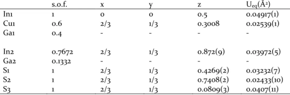
Table S8. Atom coordinates, isotropic atomic displacement parameters, and occupancy rate of each atomic sites of CIGS6 from PEDT data
s.o.f. x y z Ueq(Å2) In1 1 0 0 0.5 0.04917(1) Cu1 0.6 2/3 1/3 0.3008 0.02539(1) Ga1 0.4 - - - - In2 0.7672 2/3 1/3 0.872(9) 0.03972(5) Ga2 0.1332 - - - - S1 1 2/3 1/3 0.4269(2) 0.03232(7) S2 1 2/3 1/3 0.7408(2) 0.02433(10) S3 1 2/3 1/3 0.0809(3) 0.0407(11) Figure S2 HA
S5
Figure S3. HAADF-STEM image of a faulted crystal, highlighting the propensity of CIGSn materials to contain intergrowth defects.
S6
Figure S4. PXRD patterns of as-prepared: (a-b) CIGS4 and (c) CIGS6 compounds. The homogeneous contrast observed in the backscattered electron image confirm a single chemical composition while electron diffraction patterns attest to the existence of at least two kinds of crystals. The enlargement of CIGS4 pattern between 4-25° (see picture b) shows one (00l) reflection indexed for each polytype (different colors)
S7
Targeted
composition T(°C) Rate(°/h) Temps(h) Cooling rate(°/h precursors Cu0.4(In0.5Ga0.5)1.2S2 850 100 340* 100 Cu, In, Ga,S
Cu0.7(In0.7Ga0.3)1.1S2 850 100 340* 100 Cu, In, Ga,S
Cu0.4(In0.7Ga0.3)1.2S2 850 100 170h 100 Cu, In, Ga,S
CIGS4 850 100 48 quenched Cu2S, In2S3, Ga2S3
CIGS5 850 100 48 quenched Cu2S, In2S3, Ga2S3
CIGS6 850 100 48 quenched Cu2S, In2S3, Ga2S3
CIGS6 (sulfurization) 900 300 3 100 Cu2O, In2O3,Ga2O3 H2S
![Figure 4. [100] electron diffraction pattern, corresponding TEM image and HAADF-STEM image (on the bottom) of a faulted crystal, highlighting the propensity of CIGS n materials to contain intergrowth defects (the value n from (M (Td) ) n-2 (In (](https://thumb-eu.123doks.com/thumbv2/123doknet/11544917.296119/6.918.100.425.420.833/figure-electron-diffraction-corresponding-highlighting-propensity-materials-intergrowth.webp)
![Figure 9. XPS valence band spectra of CIGS n series and CuIn 0.7 Ga 0.3 S 2 compound in [-10-0] eV range](https://thumb-eu.123doks.com/thumbv2/123doknet/11544917.296119/8.918.137.388.743.990/figure-valence-spectra-cigs-series-cuin-compound-range.webp)