Pépite | Ingénierie de substrat par micro-usinage laser pour l’amélioration des performances de composants et fonctions RF intégrées en technologie SOI-CMOS
227
0
0
Texte intégral
(2) Thèse de Arun Bhaskar, Université de Lille, 2019. © 2019 Tous droits réservés.. lilliad.univ-lille.fr.
(3) Thèse de Arun Bhaskar, Université de Lille, 2019. UNIVERSITY OF LILLE Doctoral school : Sciences for engineering Laboratory : Institut d'Electronique, de Microélectronique et de Nanotechnologie - IEMN. THESIS Presented by Arun BHASKAR For obtaining the grade of Doctor of University Electronics, Microelectronics, Nanoelectronics and Microwave. Substrate engineering using laser micromachining for improvement of RF devices and systems integrated in SOICMOS technology Defended on 07/10/2019 in front of the jury composed of: Mrs Florence GARRELIE Professeur, Université Jean Monnet, Saint-Etienne Rapporteur Mr Pierre BLONDY Professeur, Université de Limoges, XLIM Rapporteur Mr Olivier UTEZA Directeur de Recherche CNRS, LP3, Marseille Président Mme Christine RAYNAUD Marketing Manager RF Technologies, CEA-LETI, Grenoble Examinateur Mr Jean-François ROBILLARD Enseignant-Chercheur ISEN-IEMN, Lille Examinateur Mr Emmanuel DUBOIS Directeur de Recherche CNRS, IEMN, Villeneuve d’Ascq Directeur de thèse Mr Christophe GAQUIERE Professeur, Université de Lille, IEMN Co-directeur de thèse Mr Daniel GLORIA Ingénieur R&D STMicroelectronics, Crolles Encadrant Industriel. © 2019 Tous droits réservés.. lilliad.univ-lille.fr.
(4) Thèse de Arun Bhaskar, Université de Lille, 2019. © 2019 Tous droits réservés.. lilliad.univ-lille.fr.
(5) Thèse de Arun Bhaskar, Université de Lille, 2019. Acknowledgements I am very grateful for having got this opportunity to work on a challenging project which was multi-dimensional. I would like to thank my PhD supervisors Emmanuel, Daniel and Christophe for having constantly guided me. I have received good support and encouragement to try new ideas from all three of them. This has made the thesis a very memorable and cherished experience and I am thankful for that. I would like to specially thank Emmanuel who had the oversight of my daily activities. His very approachable nature made it very easy for me to express my ideas and questions to him. He would always respond in an enthusiastic manner and spend adequate time to discuss the matter at hand. This constant support enabled me to stay motivated during the thesis. It was great to work and also have social interactions with colleagues of my group over these years: Jean-François, Maciej, Valentina, Stanislav, Jean-Marc, Thierno, Quentin, Di, Tianqi, Justine, Jun, Pascale, Jean-Michel. I was also benefitted by a lot of technical help from other members of the lab. I would like to thank the cleanroom and RF characterization technical staff, Matthieu, Flavie, Etienne, and Vanessa for their valuable contributions at different phases of PhD. Big thanks to all of my colleagues at ST Microelectronics and the RFSS team. I really liked the jovial morning coffee breaks and supportive working environment there and the team outings. A special mention of thanks to all the colleagues with their important contributions to the thesis: Cédric, Yohann, Simon, Vipin, Philippe, Jérome, Raphael. I am in gratitude for my family who always encouraged me in my pursuits of education. Heartfelt thanks to my wife Deepthi, who has been a great source of motivation for me for well over two years now. She has enabled me to gain strength and help develop my overall personality. I would also like to express my thanks to all my good friends in Lille who I had a lot of memorable moments with: Gatien, Dev, Ragini, Ankita, Richa, Inder, Tanu, Naina, Shilpa, Piyush, Spurthi, and Ashwini. I sincerely thank God who has given me knowledge that I have been blessed enough to receive. Heartfelt expressions of gratitude to my hero Swami Vivekananda and other great spiritual leaders whose words empower and embolden me to be who I am.. © 2019 Tous droits réservés.. lilliad.univ-lille.fr.
(6) Thèse de Arun Bhaskar, Université de Lille, 2019. © 2019 Tous droits réservés.. lilliad.univ-lille.fr.
(7) Thèse de Arun Bhaskar, Université de Lille, 2019. Table of contents General Introduction ........................................................................................................... 1. Chapter 1: Synergy of laser processing and SOI technology for More than Moore advancements .................................................................................................................. 5 1.0 Introduction.................................................................................................................... 5 1.1 The semiconductor industry: An overview .................................................................... 7 1.2 More than Moore: Introduction and recent advances ................................................... 9 1.2.1 Motivation...............................................................................................................10 1.2.2 SoC integration: Die level optimization .................................................................11 1.2.3 Packaging: System level optimization ...................................................................13 1.3 Laser processing: An emerging driver for More than Moore .......................................17 1.3.1 The evolution of femtosecond laser ........................................................................17 1.3.2. Application of femtosecond laser processing in More than Moore ...................18. 1.3.2.1 Packaging and integration ...............................................................................18 1.3.2.2 MEMS...............................................................................................................21 1.3.2.3 Microfluidics .....................................................................................................23 1.3.2.4 Integrated photonics ........................................................................................25 1.4 SOI Technology: A platform for SoC integration .........................................................27 1.4.1 Memory and logic ...................................................................................................29 1.4.2 RF/microwave circuits ............................................................................................30 1.4.3 Integrated photonic circuits ...................................................................................34 1.4.4 MEMS .....................................................................................................................36 Concluding Remarks ...........................................................................................................37 References ...........................................................................................................................39. Chapter 2: Towards high-end RF electronics and laser material processing: State of the art .................................................................................................................................. 43 2.0 Introduction...................................................................................................................43 2.1 Micromachining of silicon .............................................................................................45 2.1.1 Overview of methods for silicon etching ................................................................45 2.1.2 Femtosecond Laser processing: An unique tool for micro/nanostructuring of silicon ...............................................................................................................................47 2.1.3 Laser micromachining: A potential candidate for high speed and large area silicon etching ..................................................................................................................50. © 2019 Tous droits réservés.. lilliad.univ-lille.fr.
(8) Thèse de Arun Bhaskar, Université de Lille, 2019. 2.2 Inductors .......................................................................................................................52 2.2.1 Factors affecting inductor performance .................................................................52 2.2.2 Inductors on SOI.....................................................................................................55 2.2.2.1 Q-factor using different substrate resistivities and BOX thickness ...............55 2.2.2.2 Inductor on commercial SOI and impact on device performance ...................57 2.2.3 Suspended inductors ..............................................................................................58 2.3 RF Switch ......................................................................................................................59 2.3.1 Overview of different implementations and technologies .....................................61 2.3.2 Performance comparison: Bulk vs. SOI .................................................................62 2.4 Low noise amplifier (LNA) ............................................................................................65 2.4.1 LNA FoM: Bulk vs. SOI..........................................................................................65 2.4.2 LNA performance comparison by optimization of passives ...................................66 Concluding remarks ............................................................................................................69 References ...........................................................................................................................71. Chapter 3: Laser processing applied to RF functions: Theoretical background and experimental methodology ............................................................................................. 77 3.0 Introduction...................................................................................................................77 3.1 Laser processing: Essential concepts............................................................................79 3.1.1 Gaussian beam parameters....................................................................................79 3.1.2 Pulsed laser processing parameters.......................................................................81 3.2 Laser processing: Description of physical processes and timescales ...........................85 3.3 Effect of different parameters on laser processing of silicon .......................................89 3.3.1 Ambient conditions .................................................................................................90 3.3.1.1 Medium of ablation ..........................................................................................90 3.3.1.1 Substrate temperature.....................................................................................91 3.3.2 Laser wavelength ...................................................................................................92 3.3.3 Laser pulse width ...................................................................................................94 3.3.3.1 Beam distortion effect ......................................................................................94 3.3.3.2 Modification of ablation threshold ...................................................................95 3.3.4 Polarization.............................................................................................................96 3.4 Effect of ablation plume on laser processing ................................................................97 3.5 Laser processing: Description of system.....................................................................100 3.5.1 Laser source and optics ........................................................................................100 3.5.2 Optical attenuator ................................................................................................101 3.5.3 Trepan head ..........................................................................................................102. © 2019 Tous droits réservés.. lilliad.univ-lille.fr.
(9) Thèse de Arun Bhaskar, Université de Lille, 2019. 3.5.4 Galvanometric scanner.........................................................................................102 3.6 Laser processing: Experimental plan .........................................................................102 3.7 RF circuits: Description and theory............................................................................104 3.7.1 Isolation structures ..............................................................................................105 3.7.2 RF Switch .............................................................................................................106 3.7.3 Inductors ...............................................................................................................108 3.7.4 Low Noise Amplifier (LNA) ..................................................................................109 Conclusion .........................................................................................................................112 References .........................................................................................................................113. Chapter 4: Femtosecond Laser Assisted Micromachining and Etch (FLAME) for SOICMOS technology .........................................................................................................115 4.0 Introduction.................................................................................................................115 4.1 Determination of laser beam waist and threshold fluence ........................................117 4.2 Scribing of trenches in silicon .....................................................................................119 4.2.1 Galvo stability: 343 nm and 1030 nm line ...........................................................120 4.2.2 Study of trenches: 343 nm source ........................................................................121 4.2.2.1 Effect of speed ................................................................................................121 4.2.2.2 Effect of fluence ..............................................................................................122 4.2.3 Study of trenches: 1030 nm source ......................................................................123 4.2.3.1 Effect of speed ................................................................................................124 4.2.3.2 Effect of fluence ..............................................................................................124 4.2.3 Detailed study of trench parameters for optimization of milling ........................126 4.2.3.1 Average trench depth (dt)...............................................................................127 4.2.3.2 Recast layer volume (Vr) ................................................................................131 4.2.3.3 Recast layer average height (havg)..................................................................132 4.2.3.4 Average roughness of trench profile (Ra) .......................................................133 4.2.3.5 Trench width (Wt) ..........................................................................................134 4.3 Laser milling ...............................................................................................................136 4.3.1 Choice of milling pitch ..........................................................................................136 4.3.2 Determination of depth as a function of number of scans ...................................138 4.3.3 Effects of ablation plume and redeposition on laser milling ...............................139 4.3.3.1 Generation of particles ...................................................................................140 4.3.3.2 Screening of laser radiation ...........................................................................142 4.3.3 Analysis of milling quality ...................................................................................146 4.4 Femtosecond Laser Assisted Micromachining and Etch (FLAME) process ..............152. © 2019 Tous droits réservés.. lilliad.univ-lille.fr.
(10) Thèse de Arun Bhaskar, Université de Lille, 2019. Concluding Remarks .........................................................................................................154 References .........................................................................................................................155. Chapter 5: FLAME membranes for high-performance RF frontends ............................115 5.0 Introduction.................................................................................................................157 5.1 Isolation structures .....................................................................................................159 5.1.1 FLAME process parameters ...............................................................................159 5.1.2 S-parameter characterization ............................................................................159 5.2 RF SP9T switch...........................................................................................................163 5.2.1 FLAME process parameters .................................................................................164 5.2.2 DC characterization..............................................................................................166 5.2.3 S-parameter characterization ..............................................................................167 5.2.4 Large signal characterization ..............................................................................170 5.2.4.1 Measurement setup........................................................................................170 5.2.4.2 Results ............................................................................................................172 5.3 Inductors .....................................................................................................................176 5.3.1 FLAME process parameters .................................................................................176 5.3.2 S-parameter characterization ..............................................................................177 5.3.3 Modelling of inductors on membranes .................................................................185 5.4 Low noise amplifier (LNA) ..........................................................................................189 5.4.1 FLAME process parameters .................................................................................189 5.4.2 Noise figure measurement ...................................................................................190 5.4.3 Standalone input inductor measurement ............................................................191 5.4.4 Linearity measurements ......................................................................................192 Concluding Remarks .........................................................................................................194 References .........................................................................................................................195. Conclusion and perspectives .............................................................................................197 References .........................................................................................................................200. © 2019 Tous droits réservés.. lilliad.univ-lille.fr.
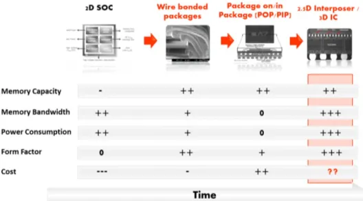
(11) Thèse de Arun Bhaskar, Université de Lille, 2019. List of Figures Fig. 1.1: (a) Cumulative revenue generated as a result of continuous scaling of feature size of semiconductor chips [3] (b) The end products of scaling at different points of time depicting the shift in high volume markets opened up as a result of Moore scaling [4] .......................................... 7 Fig. 1.2: The emergence of different paradigms of connected devices: Beginning from local area networks (LAN) connecting two or more desktop stations in a localized geographical area, the internet was born connecting computers worldwide. Advent of social media, entertainment and communication platforms enabled massive entry of people on the web. The next phase that is emerging rapidly is the Internet of Things [11]. .................................................................................. 8 Fig. 1.3: Schematic comparing the different methods of system integration [12] ............................. 9 Fig. 1.4: A real-world analogy of a system which is compared to a city. Just as different bodies of the city need to interlink and communicate with each other, an electronic system needs to optimize its functioning between the interconnected components for efficiency. [13] ................... 10 Fig. 1.5: A comparison of different integration schemes and the tradeoffs obtained between cost, performance and form factor for each type of technology.................................................................. 11 Fig. 1.6: Power management scheme on a portable electronic device depicting the typical range of voltages on the storage side and the load side [14] ............................................................................ 12 Fig. 1.7: Chip realized on BCD platform containing digital, analog, memory and High Voltage blocks [15] ............................................................................................................................................. 12 Fig. 1.8: Different packaging integration schemes (a) SiP (b) PoP (c) PiP [16] ............................... 13 Fig. 1.9: 3D stacking of two dies using Through-Silicon Vias (TSVs) for chip to chip interconnections. The four arrows point to the locations where the reliability concerns emerge in such a package. The final package is ready for board level integration using solder bumps connected to the substrate. [19] .......................................................................................................... 14 Fig. 1.10: (a) Array of TSVs realized using via-middle process flow (b) Close-up view of via (c) Cu interconnection by Cu-Cu TCB bonding (d) Cross section view of a 5 die stack [21] ...................... 15 Fig. 1.11: 2.5D packaging concept containing a silicon interposer for interconnection of dies. The demonstrated package here is a FPGA product developed by Xilinx [22]....................................... 16 Fig. 1.12: Comparison of different packaging technologies in terms of system performance metrics. [23] .......................................................................................................................................... 16 Fig. 1.13: Comparison of 3 generations of femtosecond laser systems. Systems 1-7 have already been demonstrated. The systems 8 – 10 were under development as of the publication date of the article [28] ............................................................................................................................................. 18 Fig. 1.14: Use of temporary bonding in FO-WLP (a) For backside processing of wafer (b) For die placement and packaging (c) The release process of temporary bonding material using laser irradiation [31] ..................................................................................................................................... 19 Fig. 1.15: The use of femtosecond laser for through silicon vias (a) Gaussian beam (b) Conventional Bessel beam (c) Tailored Bessel beam (d) Vias in 100 µm silicon (d) Front side of TSV array (b) Rear side of TSV array [33] ......................................................................................... 19 Fig. 1.16: Surface passive pressure sensor integrated on a thin film foil (a) Finished package (b) TGV for sensor electrical connection (c) Bonded sensor front and back view (d) Cavity in glass to create chamber for pressure reference [34] ........................................................................................ 20 Fig. 1.17: (a) Diaphragm in 4H-SiC substrate (b,c) SEM image of diaphragm milled with pulse energy 0.05 mJ and 0.15 mJ [35] ....................................................................................................... 21 Fig. 1.18: (a) Dimensions of the comb drive: a=20 µm, b=10 µm, l=21 µm, d=15 µm (b) SEM micrograph of machined microgripper [36] ........................................................................................ 22 Fig. 1.19: (a) MEMS mold fabricated in silicon (b) MEMS structures realized using micromolding of polymeric precursors [37], [38] ........................................................................................................ 22. © 2019 Tous droits réservés.. lilliad.univ-lille.fr.
(12) Thèse de Arun Bhaskar, Université de Lille, 2019. Fig. 1.20: Micromachined MEMS cantilevers in silicon [39] ............................................................. 23 Fig. 1.21: (a) Micron sized particle filter using two photon polymerization (b) Filter matrix along the microfluidic channel in fused silica using selective etching of femtosecond laser irradiated areas in HF and KOH [40], [41] .......................................................................................................... 23 Fig. 1.22: (a,b) Microfludic mixer schematic in fused silica (c,d) Microscope images of inscribed mixing channels (e,f) Fluorescence microscopy to quantify mixing [42] ......................................... 24 Fig. 1.23: (a) Electrofluidic chip schematic with external supply (b) Fabricated electrofluidic chip containing two electrodes which are baised using external supply (c) The alignment of Euglena affected in the presence of external field. Turning off the field restores the random orientation of cells [43] ................................................................................................................................................ 24 Fig. 1.24: (a) BFL fabricated on PMMA (b) 1D photonic crystal on sapphire [45], [46] .................. 25 Fig. 1.25: Fabrication of 3D high-Q resonator in fused silica with SEM images (a) Sequence of steps (b) After laser direct write and HF etch (c) After laser annealing (d) Resonator with tilted angle (e) Vertical resonator with different heights [47] .................................................................... 26 Fig. 1.26: (a) Cross-sectional view of microring resonator (b) SEM image of the resonator (c) Transmission characteristics of the resonator [48] ............................................................................ 26 Fig. 1.27: Large area microlens array fabricated on thin film silicon with average diameter (a) 20 µm (b) 30 µm with corresponding depth profiles shown on the left[49] ........................................... 27 Fig. 1.28: Transistor configurations for PD-SOI and FD-SOI [51] ................................................... 27 Fig. 1.29: Ultra thin body scaling routes for FDSOI technology [52] ............................................... 29 Fig. 1.30: (a) SPICE simulation 16-bit adder circuit on bulk and FDSOI technology (b) Frequency gain measured for LVT (low threshold voltage) and RVT (regular threshold voltage) for regular bulk, strain engineered bulk and FDSOI technologies [52] .............................................................. 30 Fig. 1.31: Transistor ft/fmax specification for different silicon based technology nodes [55] ............ 31 Fig. 1.32: (a) Schematic of DSN measurement showing 8 inverter chains on digital side (b) Measured noise power on the analog side at two different supply voltages[60] .............................. 32 Fig. 1.33: Linearity of a coplanar waveguide measured for different substrate types with transmission line of length (a) 2.1 mm (b) 1 mm [61], [62] .............................................................. 33 Fig. 1.34: (a) Schematic showing the charge state at the silicon oxide interface at different bias conditions (b) Performance comparison between eSi and HR-SOI substrate [64]........................... 34 Fig. 1.35: Optical functions on SOI substrate [67] ............................................................................. 35 Fig. 1.36: Mach Zehnder Interferometer and optical switch [69] ..................................................... 36 Fig. 1.37: Pressure sensors on SOI membranes (a) N-MOSFET suspended on membrane of area 250 x 400 µm2 (b) A current source suspended on the edge of the membrane [71] ......................... 36 Fig. 1.38: Self assembled 3D MEMS structures using CMOS compatible processes for temperature and flow sensing applications [71] ...................................................................................................... 37 Fig. 1.39: A route for RF performance enhancement by making use of local substrate removal for alleviation of substrate effects ............................................................................................................ 38. Fig. 2.1: Example of macro-sized cavities etched in silicon using (a) TMAH: Etch Rate – 1.2 μm min-1 [8] (b) Advanced silicon etching ,a variant of Bosch process: Etch Rate – 15 μm min-1 [9] . 46 Fig. 2.2: LIPSS on Titanium illustrated with SEM images taken after (a) Initial surface (b) 2 shots (c) 10 shots (d) 40 shots [10] ...................................................................................................... 47 Fig. 2.3: Color printing on stainless steel using LIPSS [11] ............................................................. 48 Fig. 2.4: (a) LIPSS on silicon (b,c,d) Structured silicon views from different angles (e) Reflectance measurements of microstructured silicon .......................................................................................... 48 Fig. 2.5: (a) Method of fabrication of nanoparticles array by ejecting nanoparticles from a parent substrate to a host substrate (b) SEM images showing the formation of nanoparticle with the application of higher laser fluences (c) Nanoparticle array fabricated on glass substrate with the inset showing a single nanoparticles [15] ........................................................................................... 49. © 2019 Tous droits réservés.. lilliad.univ-lille.fr.
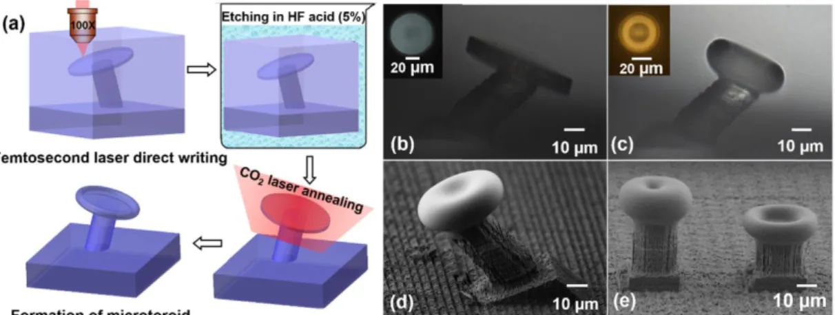
(13) Thèse de Arun Bhaskar, Université de Lille, 2019. Fig. 2.6: Examples of milled cavities in silicon .................................................................................. 50 Fig. 2.7 : (a) Inductance for varying number of turns (b) Q-factor for varying number of turns [24] ............................................................................................................................................................... 53 Fig. 2.8: (a) Characteristic dimensions of an inductor showing segments of two neighbouring turns (b) Variation of inductance, maximum quality factor and resonance frequency with variation in different dimensions and design of the inductor [24].................................................... 54 Fig. 2.9: (a) Inductance with varying substrate resistivity (indicated in legend in units of Ω.m) (b) Q-factor for varying substrate resistivity [24].................................................................................... 54 Fig. 2.10: Quality factor obtained for the use of different dielectrics [26] ........................................ 55 Fig. 2.11: (a) Q-factor for different substrate resistivities (b) Self-resonance and inductance values for different substrate resistivities [27] .............................................................................................. 56 Fig. 2.12: (a) Q-factor obtained for varying thickness of oxide layer (b) Inductance values obtained on bulk Si wafers with a oxide thickness of 25 µm [26], [28] ............................................................ 56 Fig. 2.13: (a)Parallel stacking of metal lines to improve Q factor (b) Cross section of the inductor (c) Q-factor curves for varying number of parallelly stacked metal lines indicated in parantheses for RRS (10-20 Ω.cm) and HRS (>300 Ω.cm) substrate types. [29] ................................................... 57 Fig. 2.14: (a) VCO circuit containing parallel LC tank circuit (b) Phase noise measured for different VCOs with varying Q-factor values (A) VCO-IV: Q = 52,4-metal HRS (B) VCO-III: Q = 22, 1-metal HRS (C) VCO-II: Q = 30, 4-metal RRS (D) VCO-I: Q = 11, 1-metal RRS ..................... 58 Fig. 2.15: SEM micrographs of micromachined inductors on silicon showing (a) Full removal of substrate (b) Partial removal of substrate [30], [31].......................................................................... 58 Fig. 2.16: Front end module components for LTE with switch module outlined ............................. 60 Fig. 2.17: Series shunt implementation of the switch showing transistor stacking in the series and shunt branches ..................................................................................................................................... 60 Fig. 2.18: Examples of implementation of switch on SOI technology (a) S96T: GSM only (b) 2xSP6T: GSM and LTE support [47], [48] .......................................................................................... 61 Fig. 2.19: (a) Ron and Coff as a function of stack number (b) Ron*Coff product as a function of stack number. The switch is fabricated on 0.18 µm thin-film SOI technology [47] .................................. 62 Fig. 2.20: Switch characteristics comparison of bulk vs. SOI SPDT switch on 0.25 µm CMOS process (a) Insertion loss (b) Isolation [57] ......................................................................................... 64 Fig. 2.21: (a) Folded cascode architecture with outlined circuit components representing the different inductors tuned in the design (b) Noise figure as a function of quality factor [73] .......... 67 Fig. 2.22: Effect of (a) source degeneration and (b) tail inductor on noise figure of LNA circuit [73] ............................................................................................................................................................... 68 Fig. 2.23: Effect of gate inductor quality factor on noise performance for (a) Constrained gain (b) Constrained power optimization [22].................................................................................................. 69. Fig. 3.1: Gaussian beam description showing (a) the variation of beam width along the propagation direction (b) The radial distribution of intensity at an arbitrary z-position ............... 79 Fig. 3.2: Overlap of pulse energy between successive pulses shown for displacement along a single direction of translation. The markers at 𝑥 = 0 shows the fluence contributions from previous pulses and future pulses ....................................................................................................... 82 Fig. 3.3: Dependence of accumulated fluence on the ratio of interpulse distance and beam waist showing regions of high sensitivity (region 1) and low sensitivity (region 2) .................................. 83 Fig. 3.4: Squared diameter of crater plotted as a function of pulse fluence to estimate threshold fluence for different number of pulses on TiO2 at repetition rate of 1 kHz. The inset shows the estimated threshold values as a function of number of pulses. [3] ................................................... 84 Fig. 3.5: Schematic representation of interaction between the electronic and lattice systems for (a) Femtosecond laser (b) Nanosecond laser (c) Normalized temperature profiles obtained for copper upon laser irradiation for different pulse durations using the TTM [6], [7] .................................... 86. © 2019 Tous droits réservés.. lilliad.univ-lille.fr.
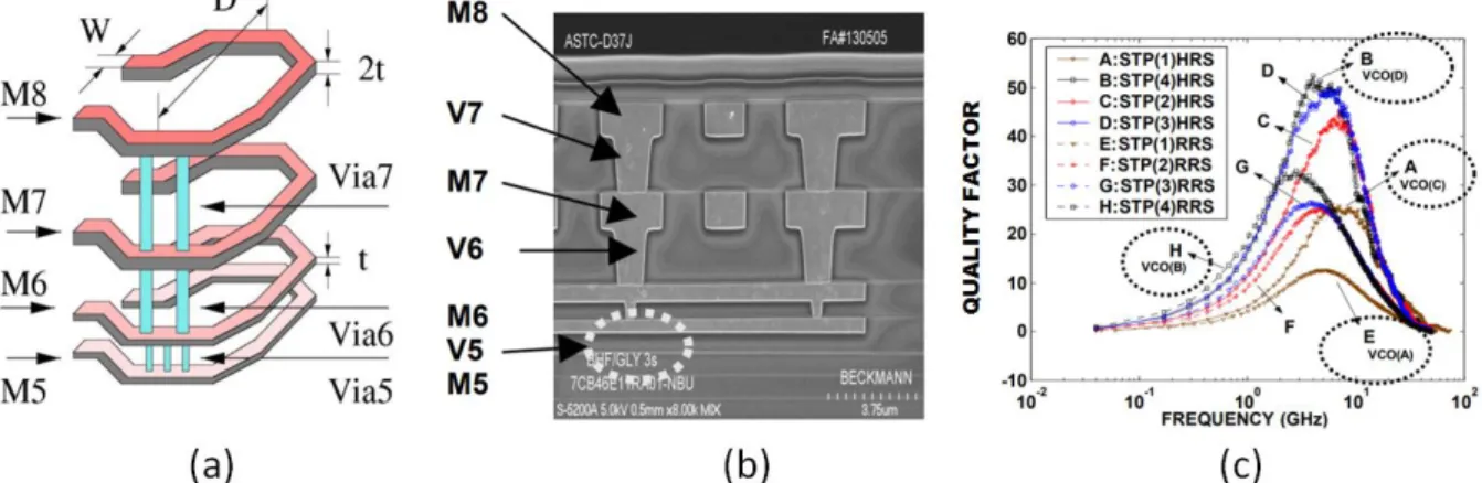
(14) Thèse de Arun Bhaskar, Université de Lille, 2019. Fig. 3.6: The summary of physical processes upon ultrashort laser irradiation and the typical timescales of these processes. The yellow region of the graph indicates the pulse duration [9] .... 87 Fig. 3.7: Graphical illustration of sequence of different physical processes due to laser irradiation on a semiconductor (a) Absorption (single and multiphoton) (b) Free carrier absorption/ Inverse bremsstrahlung (c) Impact/Avalanche ionization (d) Non equilibrium carrier distribution after excitation (e) Electron –electron scattering (f) Emission of phonons (g) Radiative recombination (h) Auger recombination (i) Carrier diffusion (j) Thermal diffusion (k) Material ablation (l) Condensation/resolidification [9] ...................................................................................................... 88 Fig. 3.8:Ablation of silicon in air, alcohol and water (a) SEM micrograph of the obtained crater for different number of impulsions (b) Threshold fluence for Np=5000 for the 3 media by squared diameter regression method [19] ........................................................................................................ 90 Fig. 3.9:Ablation threshold dependence on the substrate temperature for 3 wavelengths [20] ..... 91 Fig. 3.10: Influence of substrate temperature on effective cutting speed of wafer grade silicon [21] ............................................................................................................................................................... 92 Fig. 3.11:Ablated volume and efficiency as a function of peak fluence normalized to the threshold fluence for three different wavelengths [23]. ..................................................................................... 93 Fig. 3.12: (a) Beam energy distribution taken after focusing of laser beam in air and measuring far-field intensity of the beam. The encircled region represents the outline of the original beam. (b) Different effects occurring at long and short pulse widths. At long pulse widths, melting is severe which causes redeposited slag and at short pulse widths non-linear effects results in nongaussian energy deposition profiles and consequently enlarged ablation profiles. [17] ................. 94 Fig. 3.13:Ablation threshold of silicon in the (a) femtosecond (b) picoseconds regime [23], [25]. In (a), two ablation thresholds are mentioned. Here Fa1 refers to threshold for onset of ablation and Fa2 refers to threshold for complete surface ablation ........................................................................ 95 Fig. 3.14: Ablation efficiency of different materials studied by making grooves using a Yb: YAG thin disc laser wavelength of 1030 nm and different pulse widths [26] ........................................... 96 Fig. 3.15: Effect of polarization on the morphology of trenches micromachined in silicon (a) Polarization perpendicular to axis of the trench (b) Polarization parallel to axis of the trench (c) Circular polarization [2] ...................................................................................................................... 96 Fig. 3.16: Quality of exit holes during drilling (a) Using fixed direction of polarization showing elongation in direction perpendicular to direction of polarization (b) Dynamic polarization control with local polarization perpendicular to the tangent of the circular hole. [29] ............................... 97 Fig. 3.17: (a) Time evolution of different species of the ablation plume of silicon at a distance of 7 mm from the target surface and peak fluence of 0.5 J cm -2 (b) Yield of fast ions as a function of laser fluence (c) Yield of slow ions as a function of laser fluence [30] .............................................. 98 Fig. 3.18: Velocity distributions during ablation of silicon using different laser parameters (a) Pulse width: 0.9 ps, Wavelength: 1055 nm, Fluence = 0.75 J cm-2, Intensity: 8.3 x 10¹¹ W cm-2 (b) Pulse width : 0.1 ps, Wavelength: 780 nm, Fluence = 0.5 J cm-2, Intensity: 5.0 x 10¹² W cm-2 [31] 98 Fig. 3.19: Evolution of laser vapour plume of aluminium for a burst with varying number of pulses in the burst showing accumulation of plume with laser conditions as follows: (i) λ = 800 nm (ii) Pulse width: 110 fs (iii) Burst frequency (fp): 1 kHz (iv) Peak fluence: 260 J cm -2. Pictures take approximately 500 µs after the last pulse is applied [32] ................................................................. 99 Fig. 3.20: Schematic description of the laser system depicting the important optical components ............................................................................................................................................................. 101 Fig. 3.21: Variation of pulse energy and average power output as a function of repetition rate . 101 Fig. 3.22: Linear absorption coefficient of silicon as a function of wavelength [34] ...................... 103 Fig. 3.23: Schematic representation of an isolation structure with its characteristic dimensions shown in (a) Top view (b) Cross section showing the different SOI layers and path for signal coupling between two fingers ............................................................................................................ 105. © 2019 Tous droits réservés.. lilliad.univ-lille.fr.
(15) Thèse de Arun Bhaskar, Université de Lille, 2019. Fig. 3.24: Schematic representation of an SP2T switch showing (a) Transistor stacking and relative sizes of series and shunt branches (b) Equivalent circuit of the switch [36], [37] ........... 106 Fig. 3.25: Layout view of the SP9T switch test structure used in the study having GSGSG access. The gate and body bias is tied for all transistor stacks. One DC bias is provided for the ON stack and the second one for other 8 stacks. The different tested bias conditions are shown on the right. ............................................................................................................................................................. 107 Fig. 3.26: (a) Cross sectional schematic of an inductor fabricated on SOI wafer showing the origin of different capacitances and resistances (b) Lumped circuit equivalent for TR-SOI (c) Lumped circuit equivalent for HR-SOI. Taken from [38] .............................................................................. 109 Fig. 3.27: Typical receiver architecture showing the different components and associated gains and noise factors [39] ......................................................................................................................... 110 Fig. 3.28: (a) Transistor layout showing the implementation of the body contact (b) Circuit diagram for the common source LNA (c) Input block diagram of the LNA. [40] ........................... 110 Fig. 3.29: (a) Input stage of a common source LNA (b) Equivalent circuit for calculating the noise at the input stage of LNA [41] ........................................................................................................... 111. Fig. 4.1: (a) Squared diameter (x) plotted as a function of pulse energy for 1030 nm source. Green line is the least squares fit of the experimental data (b) Optical micrographs of ablated area shown for 4 different fluences (c) Measured diameter in x and y direction for different fluences 117 Fig. 4.2: (a) Squared diameter (x) plotted as a function of pulse energy for 343 nm source. Green line is the least squares fit of the experimental data (b) Optical micrographs of ablated area shown for 4 different fluences. Outlined region for 42.7 mJ cm -2 shows the distortion of beam and redistribution of incident energy (c) Measured diameter in x and y direction for different fluences ............................................................................................................................................................. 118 Fig. 4.3: Optical micrographs depicting evolution of laser spot with increasing laser fluence (a) 0.055 J cm-2 (b) 0.067 mJ cm-2 (c) 0.082 mJ cm-2 (d) 0.097 mJ cm-2 ................................................ 119 Fig. 4.4: 2D laser scribing at different galvo speeds for 343 nm source ......................................... 120 Fig. 4.5: 2D laser scribing at different galvo speeds for 1030 nm source ....................................... 120 Fig. 4.6: Profile of trenches taken along the centre of the trench for 343 nm source at fluence of 4.2 J cm-2 and repetition rate 200 kHz and scan speeds of (a) 25 mm s-1 (b) 50 mm s-1 (c) 75 mm s-1 (d) 100 mm s-1 ..................................................................................................................................... 121 Fig. 4.7: Profile of trenches along the centre of the trench for 343 nm source at scan speed of 100 mm s-1 and pulse repetition rate 200 kHz and fluence of (a) 3.7 J cm-2 (b) 6 J cm-2 (c) 9 J cm-2. The microscope image shows the micro-holes at the bottom of the trench............................................ 122 Fig. 4.8: Profile of trench compared with the profile of recast layer for trench scribed at 6 J cm -2. The red line is the profile at trench centre while blue line represents the recast layer profile.... 123 Fig. 4.9: Profile of trenches along the centre of the trench for 1030 nm source at fluence of 13.6 J cm-2 and repetition rate 30 kHz and scan speeds of (a) 25 mm s-1 (b) 50 mm s-1 (c) 75 mm s-1 (d) 100 mm s-1 ........................................................................................................................................... 124 Fig. 4.10: Profile of trenches along the centre of the trench for 1030 nm source at scan speed of 100 mm s-1 repetition rate 30 kHz and fluence of (a) 6.6 J cm-2 (b) 19.9 J cm-2 (c) 33.1 J cm-2 (d) 46.1 J cm-2 ........................................................................................................................................... 125 Fig. 4.11: Profile of trenches along the centre of the trench for 1030 nm source at scan speed of 30 mm s-1 repetition rate 30 kHz and fluence of (a) 6.6 J cm-2 (b) 19.9 J cm-2 (c) 33.1 J cm-2 (d) 46.1 J cm-2 ...................................................................................................................................................... 125 Fig. 4.12: Cross sectional profile of a trench .................................................................................... 127 Fig. 4.13: Average trench depth plotted as a function of fluence for 3 cases at different scan speeds ............................................................................................................................................................. 128 Fig. 4.14: Axial trench profile showing narrowing of trench and possible presence of debris ...... 130. © 2019 Tous droits réservés.. lilliad.univ-lille.fr.
(16) Thèse de Arun Bhaskar, Université de Lille, 2019. Fig. 4.15: Recast layer volume plotted as a function of fluence for 3 cases at different scan speeds ............................................................................................................................................................. 131 Fig. 4.16: Recast layer average height plotted as a function of fluence for 3 cases at different scan speeds .................................................................................................................................................. 132 Fig. 4.17: Average roughness of trench plotted as a function of fluence for 3 cases at different scan speeds .................................................................................................................................................. 134 Fig. 4.18: Inner trench width plotted as a function of fluence for 3 cases at different scan speeds. The error bars represent symmetric error of one standard deviation ............................................ 135 Fig. 4.19: (a) Cross-sectional profiles of single trench as a function of varying laser power at different scan speeds on 1030 nm source (b) Cross-sectional profiles for two lines scribed parallel to each other with varying pitch. Laser parameters: (i) Power: 0.26 W (ii) Scan speed: 20 mm s-1 (iii) Fluence: 6.4 J cm-2 ....................................................................................................................... 136 Fig. 4.20: (a) Cavity depth obtained for different squares plotted as a function of square side. Milling parameters (i) Source: 1030 nm (ii) Scan speed : 5 mm s-1 (iii) Repetition rate: 2 kHz (iv) Fluence: 56.8 J cm-2(v) Number of passes: 15 (b) Plot of depth as a function of different milling parameters for the two laser sources having average power of 1 W for square of side 1 mm. ..... 139 Fig. 4.21: Particle generation and redeposition as a function of laser fluence and pitch. Milling parameters (i) Source: 1030 nm (i) Area: 0.25 x 0.25 mm 2 (ii) Power: Column 1: 0.054 W, Column 2: 0.072 W, Column 3: 0.085 W, Column 4: 0.09 W) (iii) Scan speed: 10 mm s-1............................ 140 Fig. 4.22: Generation of particles during milling on 1030 nm source: (a) Case 1: Narrow opening, deep cavity (b) Case 2: Wide opening, deep cavity (c) Case 3: Narrow opening, shallow cavity. Large cavity milling parameters: Scan Speed - 50 mm s-1, Fluence – 61.5 J cm-2, No. of scans- 12. Small cavity milling parameters: Scan speed – 10 mm s-1, Fluence – 7.1 J cm-2, No. of scans – 80 ............................................................................................................................................................. 141 Fig. 4.23: Demonstration of presence of ablation plume in the region of ablation (a) Milling process without air flow (b) Milling process with air flow (c) Depth profiling of particle aggregates along the white dotted line. Milling parameters (i) Scan speed: 50 mm s-1 (ii) Fluence: 9.8 J cm-2 (iii) Pulse repetition rate: 100 kHz (iv) No. of scans: 50 .................................................................. 142 Fig. 4.24: Profilometer scans of milling with beam trajectory for each scan shown in the middle. Milling parameters (i) Scan speed: 100 mm s-1 (ii) Fluence: 9.9 J cm-2 (iii) Pulse repetition rate: 200 kHz (iv) No. of scans: 50 (v) Delay between successive scans: (a) 0 s (b) 1 s (c) 2 s (d) 3 s ..... 144 Fig. 4.25: Profilometer scans of 2-way milling (i) Scan speed: 100 mm s-1 (ii) Fluence: 9.9 J cm-2 (iii) Pulse repetition rate: 200 kHz (iv) No of scans: 50 (v) Delay between successive scans: (a) 0 s (b) 1 s (c) Two-way milling trajectory ............................................................................................... 146 Fig. 4.26: Milling profiles taken for two different square cavities of side 1 mm milled on two different sources and different laser parameters (a) (i) Source: 343 nm (ii) Scan speed : 100 mm s -1 (iii) Repetition rate: 200 kHz (iv) Fluence: 9.6 J cm-2 (v) Number of scans: 40 (b) (i) Source: 1030 nm (ii) Scan speed : 30 mm s-1 (iii) Repetition rate: 20 kHz (iv) Fluence: 51.1 J cm-2 (v) Number of scans: 8 (c) Plot of depth distributions along with Gaussian fit ..................................................... 147 Fig. 4.27: Morphology of the bottom of the trench after cleaning in ultrasonic bath. Milling using 1030 nm source with parameters: Single scan; Scan speed - 20 mm s-1; Repetition rate - 30 kHz; Pitch - 10 μm; Fluence (a) 2.8 J cm-2 (b) 4.7 J cm-2 (c) 12.7 J cm-2 (d) 17.4 J cm-2 ......................... 148 Fig. 4.28: Morphology of the bottom of the trench after cleaning in ultrasonic bath. Multipass milling (Depth ~ 100 μm) using 1030 nm source with parameters: Scan speed - 20 mm s-1; Repetition rate - 30 kHz; Pitch - 10 μm Fluence/ Number of scans (a) 2.8 J cm-2/65 (b) 4.7 J cm2/28 (c) 12.7 J cm-2/17 (d) 17.4 J cm-2/10 ............................................................................................ 149 Fig. 4.29: Average depth of cavities milled on the 1030 nm source at repetition rate of 30 kHz for different fluences/ number of passes indicated in the legend. Dotted and solid lines represent data before and after ultrasonic cleaning respectively ............................................................................ 150. © 2019 Tous droits réservés.. lilliad.univ-lille.fr.
(17) Thèse de Arun Bhaskar, Université de Lille, 2019. Fig. 4.30: Cavity side walls after cleaning in ultrasonic bath. Milling parameters used are scan speed of 20 mm s-1 and repetition rate of 30 kHz with fluence/ number of scans (a) 2.8 J cm -2/65 (b) 4.7 J cm-2/28 (c) 12.7 J cm-2/17 (d) 17.4 J cm-2/10 ............................................................................. 151 Fig. 4.31: Reduction of holes by changing the focus for each pass. Milling parameters: (i) Speed: 30 mm s-1 (ii) Repetition rate: 20 kHz (iii) Fluence: 51.1 J cm-2 (iv) No. of scans: 8 (iv) Focus change after each scan (a) No focus change (b) 45 μm into the sample ...................................................... 152 Fig. 4.32:FLAME process steps (1) Lamination of Etch protect layer (2) Laser milling under SOI circuit (3) XeF2 dry etching (4) Stripping of etch protect layer. (a) Hatching of area ABCD to define trajectory of laser beam (b) View of cavity obtained in area ABCD .................................... 153 Fig. 4.33: Alignment methodology for creating reference axes on backside (a) Origin (b) x-axis (c) y-axis ................................................................................................................................................... 153 Fig. 4.34: Morphology of cavity after 25 cycles of etching in XeF2 .................................................. 154. Fig. 5.1: 2-port S-parameters measurement bench ......................................................................... 160 Fig. 5.2: Isolation values before FLAME process (a) ISO-A (b) ISO-B (c) ISO-C (d) ISO-D ......... 161 Fig. 5.3: Isolation values after FLAME process (a) ISO-A (b) ISO-B ............................................. 162 Fig. 5.4: DLM images after FLAME process (a) ISO-A HR (b) ISO-A TR (c) ISO-B HR (d) ISO-B HR ....................................................................................................................................................... 162 Fig. 5.5: Difference in isolation values before and after FLAME process (a) ISO-A (b) ISO-B .... 163 Fig. 5.6: (a, c) Optical microscope images of cavities obtained for 2-step milling process of SP9T switch. (b,d) Cross sectional images of the fast and slow milling steps respectively. ................... 164 Fig. 5.7: (a) Optical micrograph of switch cavity after laser ablation (b) Profilometer scan of the ablated area with outlined region showing locally deep regions (c) After 25 cycles of XeF 2 etch. Outlined area etched first suggesting a uniform vertical etch rate of cavity (d) After 50 cycles of XeF2 etch (e) After 75 cycles of XeF2 etch (f) After 100 cycles of XeF2 etch (g) View of the switch front side using backlight illumination from the cavity side. ......................................................... 165 Fig. 5.8: DC characteristics of the RF switch on TR substrate for 2 channel lengths before and after substrate removal (a) 180 nm (b) 220 nm ................................................................................ 166 Fig. 5.9: Self heating of RF switch seen in DC characterization on TR-SOI (a) 180 nm (b) 220 nm ............................................................................................................................................................. 167 Fig. 5.10: S21 plot for two different channel lengths and bias conditions before and after FLAME (a) HR-SOI substrate (b) TR-SOI substrate ..................................................................................... 169 Fig. 5.11: S11 plot for two different channel length and bias conditions before and after FLAME (a) HR-SOI substrate (b) TR-SOI substrate .......................................................................................... 170 Fig. 5.12: Schematic of 2nd and 3rd harmonic distortion measurement bench ............................... 171 Fig. 5.13: Linearity measurement of the bench using a thru line on Calkit .................................. 172 Fig. 5.14: Harmonic distortion dependence on area of silicon etched measured at bias B1 on HR substrate ............................................................................................................................................. 173 Fig. 5.15: 2nd harmonic distortion before and after FLAME process (a) HR-SOI (b) TR-SOI. Symmetric error bars represent single standard deviation. ........................................................... 173 Fig. 5.16: 3rd harmonic distortion before and after FLAME process (a) HR substrate (b) TR substrate. Symmetric error bars represent standard deviation. .................................................... 174 Fig. 5.17: Failure of ON transistor caused by excessive self heating at high input power ........... 175 Fig. 5.18: Membrane area showing suitability for (a) Small and medium sized inductors (b) Large inductor ............................................................................................................................................... 177 Fig. 5.19: Open pad deembedding methodology .............................................................................. 178 Fig. 5.20: Measured values of self-resistance and Q-factor for the inductor on 4 different dies for HR substrate ...................................................................................................................................... 178 Fig. 5.21: Corrected values of self-resistance and Q-factor for the inductor on 4 different dies for HR substrate. Here, the contact inductance is not removed from Z ind. .......................................... 179. © 2019 Tous droits réservés.. lilliad.univ-lille.fr.
(18) Thèse de Arun Bhaskar, Université de Lille, 2019. Fig. 5.22: Inductor parameters for single turn inductors before and after FLAME (a) Selfinductance (b) Self resistance (c) Q-factor ........................................................................................ 180 Fig. 5.23: DLM images of single turn inductors taken close to the bond pad ................................ 181 Fig. 5.24: Inductor parameters for two turn inductors before and after FLAME (a) Self-inductance (b) Self resistance (c) Q-factor ........................................................................................................... 182 Fig. 5.25: DLM images of two turn inductors taken close to the bond pad ................................... 182 Fig. 5.26: DLM images of single turn inductors 1T-S and 1T-M with different bond pad configurations ..................................................................................................................................... 184 Fig. 5.27: Extracted parameters of inductors on partially removed TR pad without deembedding ............................................................................................................................................................. 185 Fig. 5.28: Pi-Model of integrated inductor on silicon technology ................................................... 186 Fig. 5.29: Models of inductors on nearly lossless substrates (a) 3-elements frequency dependent model (b) 6-elements model (c) Modified 6-elements model ............................................................ 187 Fig. 5.30: Comparison of measured vs. modelled inductor parameters ........................................ 188 Fig. 5.31: LNA layout showing the different inductors and corresponding drawn layout area for laser processing .................................................................................................................................. 190 Fig. 5.32: DLM images of suspended inductors for 3 test cases ...................................................... 190 Fig. 5.33: Comparison of (a) Noise figure with error bars representing min-max values (b) Gain before and after FLAME process ...................................................................................................... 191 Fig. 5.34: Extracted parameters of input inductor from single port S-parameter characterization for HR substrate (a) Self Inductance (b) Self resistance (c) Q-factor.............................................. 192 Fig. 5.35: Measurement setup for P1dB and IIP3 .............................................................................. 193. Fig. C.1: Coupling of light from fibre to photonic IC using grating coupler [5] ............................. 199. © 2019 Tous droits réservés.. lilliad.univ-lille.fr.
(19) Thèse de Arun Bhaskar, Université de Lille, 2019. List of Tables Table 1.1: Comparison of different laser technologies and their relative capabilities [25] ............. 17 Table 1.2: Comparison of PD-SOI and FD-SOI technologies [51] ..................................................... 28 Table 1.3: ft/fmax values of recent silicon based commercial technologies ......................................... 32. Table 2.1: Summary of standard silicon etching processes. Adapted from [1] and [2] .................... 45 Table 2.2: High throughput volume ablation rates for different materials [20] .............................. 52 Table 2.3: Performance summary of suspended inductors on different substrates. Adapted from [33] ........................................................................................................................................................ 59 Table 2.4: Ron*Coff values for different process technologies [49] ................................................... 62 Table 2.5: Performance specifications of switches realized on different technologies for GSM frequency bands ................................................................................................................................... 63 Table 2.6: Summary of LNAs realized in CMOS technologies. Adapted from [58] ......................... 65 Table 2.7: LNA designs on SOI technology. Taken from [69] ........................................................... 66. Table 3.1: Laser ablation crater study depicting ablation threshold, height and volume variation with change in laser wavelength [22] ................................................................................................. 92 Table 3.2: Summary of laser beam parameters for the 3 laser sources ......................................... 100 Table 3.3: List of characterized isolation structures and their dimensions ................................... 106 Table 3.4: Description of inductors used in the study ..................................................................... 108 Table 3.5: Summary of RF characterization performed on different RF circuits .......................... 112. Table 4.1: Parameters extracted from average trench depth using curve fitting .......................... 128 Table 4.2: Measured quantities at different values of delay for 1-way milling ............................. 144 Table 4.3: Measured quantities at different values of delay for 2-way milling ............................. 145 Table 4.4: Calculated quantities for milled cavities (single scan) on 1030 nm source at repetition rate of 30 kHz and scan speed of 20 mm s-1 ..................................................................................... 148 Table 4.5: Calculated quantities for milled cavities (multiple scans) on 1030 nm source at repetition rate of 30 kHz and scan speed of 20 mm s-1 .................................................................... 151. Table 5.1: FLAME process parameters for isolation structures ..................................................... 159 Table 5.2: Milling parameters of SP9T switch ................................................................................. 164 Table 5.3: Milling parameters for inductor study ........................................................................... 176 Table 5.4: Summary of inductor measurements .............................................................................. 183 Table 5.5: Modified 6-element model parameters for 2-turn inductors .......................................... 188 Table 5.6: Summary of LNA IIP3 measurements ........................................................................... 193 Table 5.7: Summary of LNA P1dB measurements ............................................................................ 194. © 2019 Tous droits réservés.. lilliad.univ-lille.fr.
(20) Thèse de Arun Bhaskar, Université de Lille, 2019. © 2019 Tous droits réservés.. lilliad.univ-lille.fr.
(21) Thèse de Arun Bhaskar, Université de Lille, 2019. List of Abbreviations BCD BER BFL BOX CAGR DIBL DLM DOF DSN EMC eSi-SOI FDD FD-SOI FEM FIB FLAME FoM FO-WLP GSG HR-SOI IoT IP3 ISM KOZ LAN LIPSS LNA LoC NA NF PD-SOI PiP PoP RDL RIU RO RR RRS SiP SoB SoC SOI TGV TR-SOI TSV TTM VCO WLP. © 2019 Tous droits réservés.. -. Biploar-CMOS-DMOS Bit Error Rate Binary Fresnel Lens Buried Oxide Compound Annual Growth Rate Drain-Induced Barrier Lowering Dual-Light Microscopy Depth of Focus Digital Substrate Noise Encapsulant Mold Compound enhanced Signal integrity Silicon-on-Insulator Frequency Division Duplexing Fully Depleted Silicon-on-Insulator Front-End Module Focused Ion Beam Femtosecond Laser Assisted Micromachining and Etch Figure of Merit Fan-Out Wafer-Level Package Ground Signal Ground High-Resistivity Silicon-on-Insulator Internet of Things Third-order Intercept Point Internal Stacking Module Keep-Out Zone Local Area Network Laser-Induced Periodic Surface Structures Low Noise Amplifier Lab-on-Chip Numerical Aperture Noise Figure Partially Depleted Silicon-on-Insulator Package-in-Package Package-on-Package Redistribution layer Refractive Index Unit Ring Oscillator Rayleigh Range Regular Resistivity substrate System-in-Package System-on-Board System-on-Chip Silicon-on-Insulator Through-Glass Via Trap-Rich Silicon-on-Insulator Through-Silicon Via Two Temperature Model Voltage Controlled Oscillators Wafer-Level Package. lilliad.univ-lille.fr.
(22) Thèse de Arun Bhaskar, Université de Lille, 2019. © 2019 Tous droits réservés.. lilliad.univ-lille.fr.
(23) Thèse de Arun Bhaskar, Université de Lille, 2019. General Introduction The invention of transistor and eventually of integrated circuits marks the beginning of the semiconductor industry. Gordon Moore penned the seminal paper on transistor scaling in 1965 predicting that the number of transistors in an integrated circuit doubles every year. A decade later, he revised his prediction that the number of transistors doubles every two years. This law has held remarkably true for several decades and has propelled the industry forward by enabling better performance through transistor scaling. Since the early 2000s, it was found that transistor scaling alone will not suffice for pushing the performance limits of electronic systems. Also there was a need to improve the diversity of electronic systems in order to support complex functionalities in devices like cell phones. This led to the emergence of a whole new focus area of the semiconductor industry referred to as More than Moore. This keyword is an umbrella term for all technological innovations concerning improvement of system performance and its diversity. More than Moore deals with many different aspects such as electronic packaging, 3D integration, development of MEMS, photonic ICs, sensors, energy harvesters etc. Within this broad context of More than Moore, the thesis will be focused on two specific areas: femtosecond laser processing and RF (Radio-Frequency) CMOS (Complementary Metal-Oxide-Semiconductor) technologies. The goal of the thesis is to apply laser processing on SOI (Silicon-on-Insulator) RF components like switches, inductors, LNA etc. The idea is to remove handler silicon under the active area of these components to obtain improved RF performance. Substrate coupling is an important factor in SOI RF circuits which results in degradation of performance. By removal of substrate, negative effects resulting from substrate coupling is eliminated which gives better performance. The organisation of the manuscript is as follows. In Chapter 1, the contextual background of the thesis is given in a detailed manner. More than Moore developments over the past years are highlighted. Following this, the relevance of femtosecond laser processing and SOI technology for More than Moore are discussed using numerous examples. At the end of the chapter, a schematic is provided to elaborate the goal of the thesis. In Chapter 2, the state of the art methods and technologies are reviewed within the framework of the thesis. At first, currently available methods for large area 1 © 2019 Tous droits réservés.. lilliad.univ-lille.fr.
(24) Thèse de Arun Bhaskar, Université de Lille, 2019. etching of silicon are reviewed. Then, the scope of femtosecond laser processing of silicon is considered showing the versatility of processing. The potential of high speed processing of silicon using femtosecond laser is looked at for industrial competency. After this, state of the art performance of inductors, switches and LNA on SOI technology is discussed showing its advantage over bulk technology. Furthermore, the superior performance of inductors after partial/complete removal of substrate will be demonstrated. The impact of using higher Q-factor inductors for LNA performance is reported. In a nutshell, this chapter covers the benefits of using laser processing for etching silicon and importance of substrate removal. Chapter 3 provides the necessary background theory and literature review relevant to the thesis. It begins with the definitions of different laser parameters. After this, the laser matter interaction in the femtosecond regime is illustrated. Then, the effect of choice of different chosen parameters on laser processing is discussed. The laser processing system that we use in the work is detailed and the experimental plan for achievement of substrate removal is laid out. Subsequently, the specific details of the RF components studied in this work are listed. The list of characterizations that are performed on different RF components is summarized at the end of the chapter. The results and discussion for laser processing methodology is the subject matter of Chapter 4. Initially, experiments are performed to compare milling feasibility at two different laser wavelengths. A systematic study of scribing 1D trenches is used as a basis for determining optimal laser parameters. Using the optimal laser parameters, 2D milling is performed and quality is analyzed. Finally, the Femtosecond Laser Assisted Micromachining and Etch (FLAME) process is described which uses an additional step of XeF2 gas etching to create SOI membranes. The process described in Chapter 4 is used to create membranes of different circuits mentioned in Chapter 3. In Chapter 5, the results of RF characterization of these membranes are presented. The specific implementation of the FLAME process for each circuit is also presented. For all circuits, all measurements are made before and after FLAME process to quantify the improvement that is obtained by removing the substrate. Compact modelling is also presented for the inductors to understand the frequency dependent losses resulting from metal losses like skin effect and current crowding effect after substrate removal.. 2 © 2019 Tous droits réservés.. lilliad.univ-lille.fr.
(25) Thèse de Arun Bhaskar, Université de Lille, 2019. Finally, a general conclusion is presented recapitulating all the obtained results and providing an overall picture of the studies carried out in the thesis. A few perspectives are provided for future studies involving further optimization of laser process and newer avenues in substrate removal studies.. 3 © 2019 Tous droits réservés.. lilliad.univ-lille.fr.
(26) Thèse de Arun Bhaskar, Université de Lille, 2019. 4 © 2019 Tous droits réservés.. lilliad.univ-lille.fr.
(27) Thèse de Arun Bhaskar, Université de Lille, 2019. Chapter 1: Synergy of laser processing and SOI technology for More than Moore advancements 1.0 Introduction This chapter provides the contextual background for the work that is carried out in the thesis. There are two main aspects in our study: laser material processing and Silicon-on-Insulator (SOI) technology. In a nutshell, the objective of the thesis is the utilization of laser processing for local substrate removal of SOI dies to augment the electrical performance of RF devices. The framework being set, the organization of the chapter is as follows. Initially, a brief overview of the semiconductor industry is provided, tracing the key advancements. Proceeding further, More than Moore advancements and their relevance to today’s industry requirements are discussed. This refers to the subset of technological innovations which are concerned with the overall improvement of system performance and extended capabilities like development of sensors, actuators, power harvesters, analog/RF modules, biochips etc. We then demonstrate how laser processing can be an effective tool which offers several solutions for the More than Moore domain. The same discussion is extended to Silicon-on-Insulator (SOI) technology, which is relevant to both Moore scaling and More than Moore applications. It will be seen that both technologies can provide solutions for functional diversification and system performance improvements. At the end of the chapter, the potential impact of two worlds working together is highlighted.. 5 © 2019 Tous droits réservés.. lilliad.univ-lille.fr.
Figure
![Fig. 1.7: Chip realized on BCD platform containing digital, analog, memory and High Voltage blocks [15]](https://thumb-eu.123doks.com/thumbv2/123doknet/3553029.104098/34.892.215.685.833.1097/realized-platform-containing-digital-analog-memory-voltage-blocks.webp)
![Fig. 1.31: Transistor f t /f max specification for different silicon based technology nodes [55]](https://thumb-eu.123doks.com/thumbv2/123doknet/3553029.104098/53.892.118.788.550.985/fig-transistor-specification-different-silicon-based-technology-nodes.webp)
+7
![Fig. 1.33: Linearity of a coplanar waveguide measured for different substrate types with transmission line of length (a) 2.1 mm (b) 1 mm [61], [62]](https://thumb-eu.123doks.com/thumbv2/123doknet/3553029.104098/55.892.125.788.224.616/linearity-coplanar-waveguide-measured-different-substrate-transmission-length.webp)
![Fig. 2.2: LIPSS on Titanium illustrated with SEM images taken after (a) Initial surface (b) 2 shots (c) 10 shots (d) 40 shots [10]](https://thumb-eu.123doks.com/thumbv2/123doknet/3553029.104098/69.892.194.701.508.858/lipss-titanium-illustrated-images-taken-initial-surface-shots.webp)
![Fig. 2.10: Quality factor obtained for the use of different dielectrics [26]](https://thumb-eu.123doks.com/thumbv2/123doknet/3553029.104098/77.892.199.700.544.754/fig-quality-factor-obtained-use-different-dielectrics.webp)
![Fig. 2.17: Series shunt implementation of the switch showing transistor stacking in the series and shunt branches [75]](https://thumb-eu.123doks.com/thumbv2/123doknet/3553029.104098/82.892.115.789.669.938/series-implementation-switch-showing-transistor-stacking-series-branches.webp)
Documents relatifs