OATAO is an open access repository that collects the work of Toulouse researchers and makes it freely available over the web where possible
Any correspondence concerning this service should be sent
to the repository administrator: [email protected]
This is a Publisher’s version published in:
http://oatao.univ-toulouse.fr/24669
To cite this version:
Venkat Sunil Kumar, Channam and Maury, Francis and Bahlawane, Naoufal Vanadium Oxide as a Key Constituent in Reconfigurable Metamaterials. (2019) In: Metamaterials and Metasurfaces. IntechOpen, 1-26. ISBN 978-1-78984-842-7
Vanadium Oxide as a Key Constituent in
Reconfigurable Metamaterials
Channam Venkat Sunil Kumar, Francis Maury and
Naoufal Bahlawane
Additional information is available at the end of the chapter http://dx.doi.org/10.5772/intechopen.80476
© 2016 The Author(s). Licensee InTech. This chapter is distributed under the terms of the Creative Commons Attribution License (http://creativecommons.org/licenses/by/3.0), which permits unrestricted use, distribution, and reproduction in any medium, provided the original work is properly cited.
Reconfigurable Metamaterials
Channam Venkat Sunil Kumar, Francis Maury and
Naoufal Bahlawane
Additional information is available at the end of the chapter
Abstract
Tunable materials are paving the way towards improved functionality of metamaterials. Vanadium oxide (VO2) with its prototypical near-room-temperature transition between phases featuring greatly contrasting electrical and optical behavior is an appealing can-didate as an active component in metamaterials. However, it is seldom known that VO2 in itself has metamaterial characteristics. VO2 under certain temperature conditions dem-onstrates a phase coexistence enabling highly tunable electrical and optical properties. In this chapter, we describe how VO2 in its hysteretic region behaves as a smart responsive Metasurface with cutting edge applications.
Keywords: metasurfaces, smart metamaterials, vanadium oxide, semiconductor to metal transitions
1. Introduction
The ability to tune, alter and switch the properties of materials is rarely offered by nature. Smart materials are a special class of materials that have the ability to alter and change their behavior depending on external stimuli. Metamaterials are artificially engineered materials featuring properties that are not readily available in nature, and which might sound non-intuitive. This includes surfaces with changing refractive index achieved by modifying the plasmon resonances of the nanostructures, or metal structures on thin dielectric layers, which the properties can be controlled by external stimuli. “Phase change” materials are the quintes-sential part for such a smart switching behavior [1].
© 2018 The Author(s). Licensee IntechOpen. This chapter is distributed under the terms of the Creative Commons Attribution License (http://creativecommons.org/licenses/by/3.0), which permits unrestricted use, distribution, and reproduction in any medium, provided the original work is properly cited.
Chalcogenides are used in optical recording media for several decades, providing efficient and reproducible changes in optical properties in response to phase transition. This function-ality is the result of phase transitions from crystalline to amorphous states and is typically triggered by a thermal, electrical or optical stimulation. Nanoscale electro-optical metamate-rial switch using chalcogenide matemetamate-rials has also been demonstrated [2–6].
Switchable metamaterials based on arrays of micro- and nanoelectromechanical (MEMS/ NEMS) systems were also being developed. Typical metamaterials consist of arrays of metal structures called as split ring resonators (SRR). These structures are typically much smaller than the desired operating wavelength and are embedded in a dielectric material. In simple terms, the unit cell of the SRR array is designed to be an inductor-capacitor (LC) circuit, where the gap between the two ends acts as a variable capacitor or inductor as a function of the frequency [1].
Active metamaterial designs are focused on changing the capacitance in the SRR gap to modu-late the amplitude of the resonance. Integrating materials with tunable electrical or optical properties into SRR allows a further control over the resonant response in metamaterials [7–11]. Consequently, phase change materials are promising candidates as they exhibit a dramatic change in their electrical and optical properties resulting from a structural phase transition [12]. When paired with SRR like Metasurfaces, they can enhance the functionality multifold.
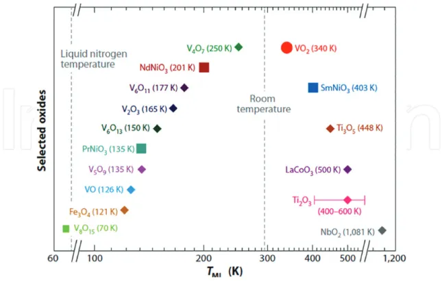
Figure 1 shows a non-exhaustive list of phase change materials plotted against their phase
transition temperatures. Interestingly oxides of vanadium form a significant number among
them and VO2 in particular has the nearest transition to room temperature. This motivates
the immense research and investigation over VO2 for its electrical and optical properties [13].
Figure 1. A non-exhaustive list of various phase change materials plotted against the temperature at which they undergo
2. Semiconductor to metal transition in vanadium oxides
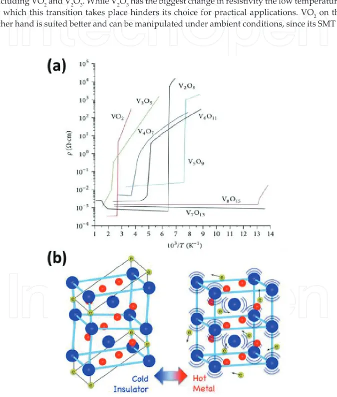
Many vanadium oxides show semiconductor to metal/metal to insulator transition SMT/
MIT characteristics. These include VO2, V2O3 and most of the so called magneli phases [14].
Figure 2(a) shows the electrical resistivity versus temperature for several oxides of vanadium,
including VO2 and V2O3. While V2O3 has the biggest change in resistivity the low temperature,
at which this transition takes place hinders its choice for practical applications. VO2 on the
other hand is suited better and can be manipulated under ambient conditions, since its SMT is
Figure 2. (a) Semiconductor to metal transition in several vanadium oxide phases and (b) changes in the electronic
properties and lattice structure (V blue; O red) of VO2 during its SMT. Above 67°C (hot state), lattice vibrations (phonons) lead to a rutile tetragonal system with freed up electrons (yellow) making VO2 behave as a metal. Once the temperature is lowered (cold state), VO2 becomes insulating due to the localization of electrons in the distorted monoclinic structure.
nearest to room temperature [15]. Figure 2(b) shows the schematic representation of the VO2 crystal during the phase transition from semiconducting monoclinic to metallic rutile phase.
In single crystals, the resistivity change reaches a factor of 105 over a very short temperature
range [16]. Hysteresis associated with this transition is of about 3 K. The large electrical
con-ductivity change and the narrow hysteresis are very good indicators of the VO2 quality. Small
stoichiometry deviations affect substantially the sharpness of the transition and increase the hysteresis width. The crystalline state of the material has an influence as well; typically, poly-crystalline materials have a broader transition than single crystals. The transition temperature also depends on the crystalline state and oxygen stoichiometry [17].
3. Responsive metamaterials with VO
2as an active component
The Split-ring resonators SRR are the most common and best characterized implementation of electromagnetic metamaterials. They respond resonantly to in-plane electric fields, and out-of-plane magnetic fields. SRR’s are the basis for many metamaterial designs due to the ease of fabrication and modeling. Each SRR has a distributed inductance, and capacitance, arising from the built-up charge at the notch. The choice of materials and the resonator dimensions determine the resonant frequency of the metamaterial [18].
Tunability of metasurface and the ability to reconfigure metadevices have attracted an immense amount of research in recent years. While the hunt for new kinds of metamaterial is still ongoing, the ability to tune and reconfigure existing metamaterial devices has attracted a significant amount of interest. Tunable metamaterials based on nonlinear components depend on the aspect of tuning the constituent materials. Several nonlinear materials, like phase change materials, liquid crystals, and III–V semiconductors etc., are readily available for real world applications and some of them are compatible and complementary with the mature metal–oxide–semiconductor (CMOS) fabrication technology. The present article describes
one such nonlinear phase change material VO2, and its application in tuning metadevices and
later demonstrating that VO2 can act as a metamaterial in itself [19].
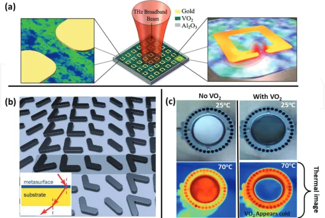
Recent developments in so called hybrid SRR configurations involving VO2 as a key
com-ponent has attracted a lot of attention (Figure 3a). The interaction of the VO2 and SRR layers
makes this hybrid metamaterial interesting. The VO2 film, thus, becomes an integral part of
this effective material layer, due to its close proximity to the SRRs and thin size compared to periodic nature of the array. Resulting in a hybrid metamaterial that mixes the proper-ties of vanadium oxide with discrete SRR array. Hybrid metamaterial devices operating at
THz frequencies were fabricated by combining double SRRs with phase changing VO2 films.
By thermal triggering of the resistivity change of VO2, the behavior of the SRR gap can be
adjusted from capacitive to resistive in order to modulate the THz beam transmission at their resonance frequencies [20–23].
The concept of Infrared adaptive camouflage, is an additional example of metamaterials-based
a heated VO2 coating above the transition temperature appears to be colder relative to the surroundings. This unique property was proposed to develop smart clothing when fabrics are
weaved with VO2 networks as shown in Figure 3c [24, 25].
Another interesting advancement in the use of metasurface (Figure 3b) is the concept of pla-nar metalens [26, 27], which are optically designed Metasurfaces for wave Front Engineering. These devices can provide local phase, amplitude and polarization control of light along the surface using optical resonators. With such metasurface a new class of flat, compact and broadband components such as lenses and polarizers can be realized beyond conventional diffractive optics. Patterned subwavelength metallic Nano antenna arrays can provide the basis for optical devices with sub-wavelength thicknesses.
4. Vanadium oxide (VO
2): A metamaterial in itself
Considering VO2 as a classic metamaterial may appear inappropriate to a certain degree.
However, if we draw the attention to the intermediate region near the vicinity of the SMT, there is a naturally occurring disordered state. This disordered state, which comprises both semiconducting and metallic phases, is highly tunable and responsive. The percentage or the
Figure 3. (a) A hybrid metasurface with gold SRR fabricated on top of a phase change material (VO2). Here VO2 is the active component of the metasurface. (b) a planar meta lens that is made of precisely fabricated structures on size with the order of the wavelength of the incident radiation and (c) apparent cooling of the VO2 coated cloth on the right even after heating above the 70°C. Image reproduced with permissions form the original publisher.
phase fraction of one in respect to the other is highly controllable and tunable via external
stimuli. This particular state of VO2 is called the naturally occurring disordered metamaterial,
and was previously termed differently by various authors.
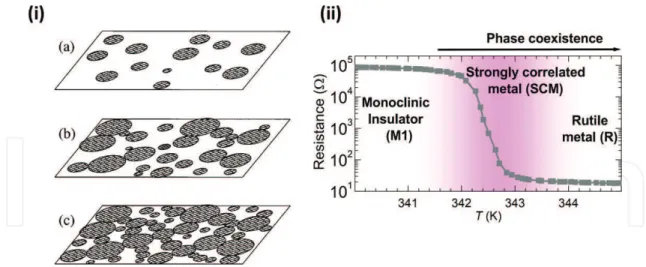
One of the early descriptions of the nature of the material in the range of phase co- existence was proposed in 1996 [28]. Authors have described the transition state as an “Inhomogeneous composite medium” composed of metallic and insulating grains. Using a “composite medium model” authors simulated the formation and clustering of the metallic domains. When the
temperature (T) exceeds the transition temperature (Tc) the conducting clusters grow and
form conducting paths throughout the film (percolation) as shown in Figure 4.
Later Kim et al. referred to the same region of phase co-existence as “monoclinic and corre-lated metal” (MCM) in 2006 [29], while Qazilbash et al. named it “strongly correcorre-lated metal”
(SCM) [30]. The shaded region in Figure 4(ii) represents this state in VO2 over a finite
tem-perature range in the transition region.
Kats et al. [31, 32] coined the term “naturally disordered metamaterial” and put forward the following arguments.
1. In the VO2 transitional state, the film comprises nanoscale structures of metallic- and
insu-lator-state VO2, and the resulting medium behaves as a “tunable disordered metamaterial.”
2. Metallic puddles of nanoscale dimensions emerge inside the dielectric phase of VO2, these
puddles then grow and coalesce, eventually leading to a fully metallic state upon transi-tion. The size of these metallic puddles is of the order of infrared frequencies. Temperature-sensitivity of these metallic structures allows for a control of the ratio between metallic and
semiconducting phases, thus VO2 can be viewed as a “natural, reconfigurable, disordered
metamaterial” with variable effective optical properties across the phase transition”
Figure 4. (i) Schematic diagram of the phase change in the VO2 film. The metallic domains nucleate sporadically (a) and as the temperature approaches TC (b), the domains grow larger and cluster. Percolation occurs above TC (c). (ii) the phase diagram of VO2 and the resistance-temperature curve showing the insulator-to-metal transition. The shaded area highlights the strongly correlated metal (SCM) region. Image reproduced with permissions form the original publisher.
3. The co-existence of metallic and insulating phases during the phase transition results in
widely tunable optical properties. Here manipulating the naturally occurring nanoscale
metallic structures in the SMT region can be imagined as a “reconfigurable disordered
metamaterial”. One key application for such transition is tunable optical switching in the
NIR region.
Lastly Zhang et al. [33] described the growth of metal nanoparticles in a dielectric matrix as aperiodic or disordered yet still offering the functionality of near “perfect metamaterial
absorbers” (PMA). Authors successfully show that neither ordered lithographical
nanostruc-tures nor self-assembled colloidal magnetic nanoparticles are necessary to attain
“control-lable metamaterials” as surfaces with controlled-reflectance or tunable PMAs (Figure 5).
The similarity between the surface structure of materials shown in Figures 4(i) and 5(ii) is striking. This and the most recent investigations legitimate, to our sense, the description of vanadium oxide operating in the narrow window of the phase co-existence as a disordered
metamaterial. The following sections will emphasize few ways in which VO2
metamate-rial region can be used to demonstrate some key application possibilities utilizing its high responsivity.
Figure 5. (i-a), Illustration of a near perfect metamaterial absorber (PMA) with random non-prefabricated metal nano
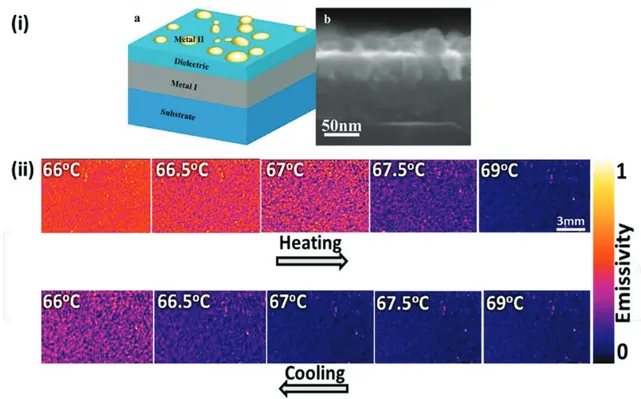
particles. (i-b), Cross-sectional view of the PMAs with random Au-NPs layer constructed on the ZnO/Ag bi-layer structure [33]. (ii) Infrared images of VO2 undergoing phase transition in the metamaterial region, showing the formation, percolation and coalescence of the metallic puddles (blue dots). The emissivity of the surface decreases on phase transition due the IR reflecting property of the rutile VO2. Image reproduced with permissions form the original publisher.
4.1. Temperature controlled electrical resistivity switching
The disordered metamaterial state of VO2 is very stable [34], as long as the surface is
main-tained at a constant temperature within the hysteresis region. The phase fraction of semicon-ducting to metallic remains undisturbed. Subsequently, it is effectively conceivable to balance out the metamaterial at any level inside the hysteresis band by controlling the temperature. A useful utilization of this behavior could be a thermally triggered electrical switch [35], which may work by providing tiny yet instantaneous heat pulses as well as cooling pulses of small amplitudes of the order of (1–3 K). These temperature inputs convey the metamaterial to cycle between resistive “Off” and conductive “On” states while keeping a similar base temperature around the phase transition window.
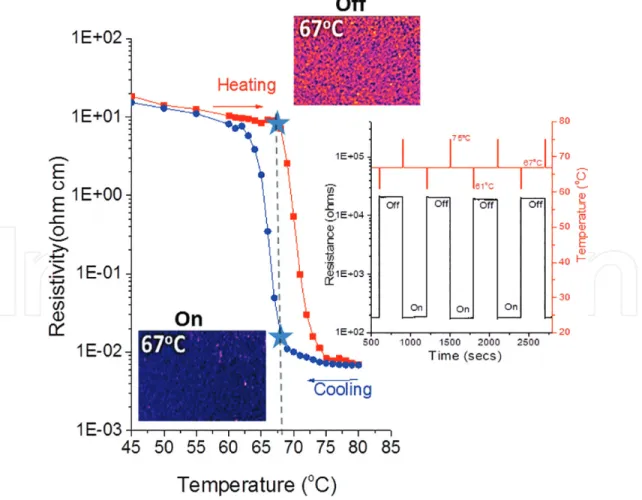
Thermally controlled electrical resistivity switching behavior of VO2 is displayed in Figure 6.
At a constant temperature of 67°C, VO2 films are stabilized at the disordered metamaterial
structure. This temperature is provided using a heating stage while simultaneously moni-toring the electrical resistance. This highly resistive state is considered as an “off” state. A quick heating pulse of ΔT ~ 3 K drives the coalescence of the metallic rutile domains, to make the film conducting. Soon after which it is retained by the stabilization of the temperature at 67°C. This difference in temperature arises from the hysteretic temperature difference
Figure 6. Thermally-driven switching of the VO2 disordered metamaterial. The “off” and “on” states are determined
by the sudden drop or increase in electrical resistance because of small changes in the temperature given in the form of thermal activation pulses as shown in the inset. Image reproduced with permissions form the original publisher.
between the forward and in reverse phase transition temperatures because of hysteresis width as detailed schematically in Figure 6. The metamaterial is driven to a high resistance “off” state by providing a cooling pulse, which encourages the shrinkage and confinement of the metallic domains. Consequently, the metamaterial features a resistive semiconducting behavior even when it relaxes back to 67°C. Hence, tiny accurate temperature inputs are
reli-ably implemented for abrupt resistivity switching of VO2. The strength of the thermal pulse
has a direct impact on the response of VO2 metamaterial. This kind of temperature inputs in
the form of short pulses allows VO2 to achieve a highly resistive “off” state or conducting “on”
state at the same steady state temperature. Furthermore, the resistance switching profiles can
be altered by providing the VO2 films with varying cold and hot temperature pulses as
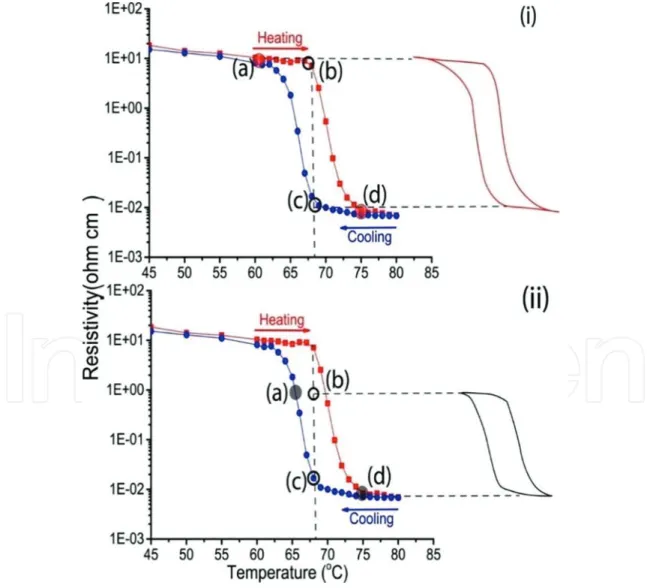
illus-trated in Figure 7.
Using stronger thermal activation pulse as shown in Figure 7(i) allows the “on” and “off” states of the system at points (b) and (c) respectively, take benefit of enhanced resistivity change. Whereas a weaker thermal activation pulse as shown in Figure 7(ii) dampens the
Figure 7. The schematic of thermal switching process based on the hysteresis curve. The result of implementing two different amplitudes of the thermal activation is illustrated in (i) and (ii). c → a → b: Cooling pulse; b → d → c: heating pulse. Image reproduced with permissions form the original publisher.
amplitude of switching. This enables better control of the metamaterial to program almost any desired switching pattern. Such an extent of adaptability demonstrates the usability
and unwavering quality of this thermally activated electrical resistivity switching in VO2
metamaterial.
It is worth noting that sharp transition with a minimal hysteresis width of ΔT = 3 K is neces-sary to attain high switching amplitude while implementing a small thermal activation. The effectiveness of such metamaterial will substantially enhance, provided a reliable approach is developed for the tuning of the SMT temperature without affecting its quality in terms of amplitude, sharpness, and hysteresis width.
4.2. Negative thermal emissivity control and smart cermet concept
Thermally triggered emissivity modulation is emphasized in this section. The low
tempera-ture semiconducting phase of VO2 features high thermal emissivity and infrared
transmis-sion. This transition occurs in a narrow temperature range of (64–68°C) where VO2 films
have the coexistence of both metallic and semiconducting phases. This, kind of disordered metamaterial state is similar to a cermet. With the increase in temperature, metallic inclusions nucleate and grow inside the dielectric (Semiconducting) phase [30, 35, 36]. Therefore, a
con-cept of “smart cermet” with tunable optical properties based on disordered VO2 metamaterial
is introduced.
The concept of tunability is addressed by accurate temperature dependent control of the dimension and density of metallic particles in the dielectric matrix, which result in the
varia-tion of emissivity of the coating. An interesting aspect of VO2-based smart cermet is that,
both metallic and dielectric entities are composed of one and the same material albeit at two
different phases. Hence, just a singular layer of VO2 can be engineered to express (i) a fully
dielectric state, (ii) a variable state with metallic inclusions embedded in the dielectric matrix, or (iii) a complete metallic state by simple temperature adjustments. This kind of flexibility is unheard of with conventional cermet coatings.
A thermal camera was employed to investigate the phase transition from semiconducting monoclinic to the metallic rutile that occurs with thermal cycling. Upon heating, the sur-face appears colder above the transition due to thermal emittance of the metallic phase. This
behavior is termed as negative differential thermal emittance. During the heating step, VO2
undergoes an abrupt semiconductor to metal transition (SMT) at 67.5°C resulting in a drop of emissivity from 0.8 to 0.1 within a narrow ΔT of 2°C. The images in Figure 8(i), (ii) and (iii) provide a visual representation of the material undergoing SMT, by formation of metallic puddles in the semiconducting phase, which grow in number and coalesce, thus converting the whole layer metallic. These metallic puddles lower the overall emissivity by reflecting the infra-red radiation.
While cooling, the emissivity abruptly rises and peaks up to 0.94 at 63.5°C marked as region (a) in Figure 8. This peculiar rise of emissivity is quite reproducible and is systematically observed in all our films. At 63.5°C the density and size of the metallic inclusions align in such a way that a near perfect thermal emittance is reached. This rise in emissivity from 0.8 to 0.1
(ΔƐ = 0.7), or 0.94 to 0.1(ΔƐ = 0.84) using VO2 coatings, is unprecedented with conventional variable emissivity coatings. Such a negative differential thermal emittance was previously
reported and VO2 was shown to operate both as perfect emitter and absorber in a tunable
phase change material. The short rise in the emissivity during the cooling cycle is correlated to the formation of nanoscale metallic inclusions in a configuration that enhances light absorp-tion [37–41].
Perfectly reversible and reliable emissivity transition is recorded for VO2 films during
extended thermal cycling tests. Furthermore, the transition characteristics were shown to be immune to the cycling rate. The stability of the metamaterial state was observed upon an extended Raman mapping of the mixed phase region over 100 hrs [34].
The reproducible behavior is in line with the ramp reversal memory effect in VO2 reported
recently [42], where the nucleation of the metallic puddle during the heating cycle occurs at the same spot over successive cycles. Upon temperature cycling, IR imaging reveals the nucle-ation of the metallic phase exactly at the same positions and confirms its systematic growth in an identical manner as the preceding heating cycle for consecutive cycles. This behavior is of paramount importance for a tunable and reliable light modulation.
VO2 metamaterial coatings provide enhanced flexibility versus traditional cermet coatings
which have a fixed density and distribution of metal particles. Guo et al. [39] presented how metallic inclusions can be modified to impact light-matter interaction. Authors investigated the applications of metallic inclusions as light trapping sites for solar energy-harvesting.
Figure 8. Temperature-dependent emissivity of VO2 across the SMT and the infrared images of three selected regions (a-i, b-ii and c-iii) on the hysteresis curve. Metamaterial region is shown as a shaded area on the hysteresis curve. Image reproduced with permissions form the original publisher.
Hence by controlling the size, shape and density of metallic inclusions in the
metamate-rial state, VO2 coatings clearly presents itself as versatile and an attractive alternative. The
property of tuneable emissivity opens up many possibilities for the design and integration of smart functionalities through innovative light modulation existing technologies.
Figure 9(i) shows tuning of emissivity by controlling the heating and cooling cycles. Choosing
to limit the extent of cooling to the temperature that enables the maximum emissivity (marked by a blue circle in Figure 9(i-b) and restarting the heating stage in the subsequent cycle in
Figure 9(i-c), one can take benefit of the observed emissivity spike to further enhance the
amplitude of the emissivity. Such control of temperature cycles yields tunable emissivity
of VO2 metamaterial between 0.94 and 0.1. Figure 9 (i-d, e and f) illustrates an example of
how the emissivity can be controlled between 0.1 and ≤0.94, by selecting the temperature of cooling down at any intermediate value. Similar approach can be utilized to change emis-sivity from 0.94 to 0.1 simply by adjusting the temperature in the heating cycle as shown in Figure 9(ii). The memory effect mentioned earlier, helps us to maintain the system at a set value of emissivity even after consecutive cycles. Therefore, the temperature is a reliable parameter to precisely control cermet architecture. Temperature cycles can be conveniently
Figure 9. Variable emissivity as shown from (i-a) to (i-f) is achieved by adjusting the minimal temperature of cooling
cycle and beginning the subsequent heating cycle immediately. Precise emissivity state can be reached by adjusting the cooling and heating temperature. Image reproduced with permissions form the original publisher.
designed to adjust the upper and lower limit of emissivity values within the 0.1–0.94 range. In terms of application, a light modulating devise with rapid transitions can also be designed,
since switching in VO2 occurs at picosecond time scale [43].
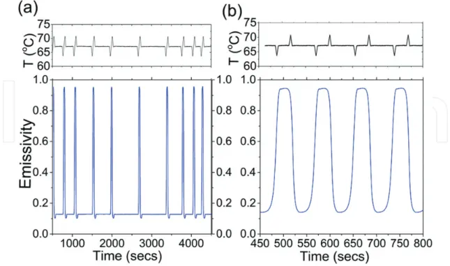
Thermally controlled switching of emissivity in VO2 films is demonstrated in Figure 10(a).
Initially VO2 films are stabilized at a steady temperature of 68°C in the metallic state with
low emissivity. A programmed cooling pulse of ΔT = 1.5°C decreases the temperature of the system to 66.5°C, driving the system to from a low emissivity state at Ɛ = 0.1 to a high emis-sivity of Ɛ = 0.94.
Temperature increase via a programmable heating pulse of identical amplitude pushes the
system to the lower emissivity. This way, VO2 metamaterial state can be used as an optical
switch with controlled emissivity stages that correlate directly with the infrared reflection property. The concept of smart cermet could be envisaged for applications such as an infra-red shutter and for emissivity modulation.
A slightly different switching profile is shown in Figure 10(b). Switching emissivity is achieved by providing tiny temperature inputs in either direction by maintaining the system at a steady temperature in the middle of the hysteresis loop. Small temperature inputs lead to large changes in emissivity, thereby leading to efficient and low power consuming alternative to already available emissivity control mechanisms.
Micro fabrication and additional processing challenges like multilayer deposition, MEMS fabrication and patterning coatings are requiring for coatings to have emissivity control and
infrared modulation [44, 45]. Infrared reflection in VO2 coatings is an intrinsic one, which
Figure 10. Thermally-controlled emissivity switching with double thermal pulses of ±1.5°C amplitude, without (a) and
means in order to achieve light modulation no further processing or fabrication steps are nec-essary. Remarkable emissivity change is produced by tiny temperature inputs. These changes
in emissivity are a direct result of the changes occurring in the topography of VO2 metasurface.
Therefore, a tunable yet modular emissivity state is achieved by changing the dimension, den-sity of metal inclusions into a semiconducting matrix, ultimately functioning as a smart cermet.
4.3. Localized phase change and IR reversible patterning
Now that we have established VO2 films when operating in the region of transition
tempera-ture (TC) behaves as a naturally disordered metamaterial. Physical properties related to the
material like resistivity, reflectivity and emissivity can be altered depending on extent of
phase transition. Through simple temperature control VO2 might exhibit contrasting
behav-iors depending on the state at which the metamaterial is set to operate. Figure 11 shows the three states namely, a high emissivity monoclinic state at 66°C, a reconfigurable emissivity metamaterial state around 66–69°C and lowered emissivity rutile state above 69°C.
As the metamaterial region manages to be stable as long as it is held at the required
tempera-ture, it’s viable to locally alter the phase of VO2 to either monoclinic or rutile depending on
the nature of temperature stimulus. Such localized phase transition can be observed evidently with a thermal Infrared camera due to significant changes in the IR reflectivity and emissivity of between the two phases. Therefore, the metamaterial can be designed to have localized phase transformations by the usage of precise temperature changes in specific areas as shown in Figure 12.
Multitude of ways can be hypothesized to enforce a localized and restricted phase change in
VO2. For the ease of understanding, we restrict these operations to those that result in
local-ized temperature manipulations that can trigger SMT in VO2 at the exact point of contact.
However, in this discussion we will focus on localized laser heating for modification of metamaterial.
Local laser heating provides a contactless method to locally change the phase of the meta-material. It is a non-invasive way of pattern transfer. By adjusting the power and focus of the laser one can achieve localized heating, this technique is easily scalable very convenient. As shown in Figure 13, patterns or words can be made by simply moving the laser across
the VO2 meta state that is kept at a constant temperature on the edge of phase transition.
The localized heating provided by the laser results in the selective phase transition resulting in desired pattern or shapes. Although the patterns are invisible to naked eye, they however are clearly visible under infrared imaging. A simple temperature cycle of heating above the Tc and cooling back to the metamaterial state erases the pattern and reset the surface for next use. Thus, resulting in a so called Infrared black board.
Several concepts of achieving localized phase transition in VO2 metamaterial are presented
in this article. Making patterns with contrasting electrical and optical properties on the same material whilst maintaining both of them stable with the use of temperature modulation will open numerous application possibilities for future Opto-electronic devices, that take advan-tage of high speed optical switching and finds use in cutting edge applications such as emis-sivity regulation, infrared camouflage, and infra-red tagging for identification.
Figure 12. Controlling the VO2 metasurface in hot or cold state by localized phase transformation.
Figure 13. Images from an IR camera showing the laser drawn pattern (LIST) undergoing the display erase and
reset process, controlled by temperature cycling. The pattern disappears as the steady state temperature is above 69°C. Lowering the temperature to 66°C resets the system and primes for new a pattern.
5. Conclusions
In conclusion this article shows vanadium oxide as a versatile material that can be used in
multiple applications. VO2 has the potential to be a suitable candidate for smart applications,
thanks essentially to its SMT behavior. Functionality of conventional Metasurfaces can be
improved multifold by incorporating a VO2 sublayer in the device. The variety and ease at
which VO2 layers can be integrated to metamaterial makes it an ideal candidate for future
optoelectronic devices and smart responsive metasurfaces.
Looking further deep into the mechanism of the SMT in VO2 reveals an interesting facet of
these films. The narrow hysteretic region near phase transition, comprising electrically and
optically contrasting media, makes VO2 by itself a promising metasurface. This naturally
occurring disordered state can be controlled with accurate temperature inputs and the ratio of the semiconducting to metallic parts can be configured spatially over the whole surface or selectively on a part of the metasurface. The rich physics involved in this phenomenon will help to further understand the mechanisms of phase transitions in the fundamental point of view whereas, the unique properties displayed by the material will inspire application pos-sibilities new generation of semiconducting devices.
Conflict of interest
The authors of this chapter indicate no conflict of interest.
Author details
Channam Venkat Sunil Kumar1*, Francis Maury2 and Naoufal Bahlawane3
*Address all correspondence to: [email protected]
1 SPIN Laboratory, Department of Physics, University of Liege, Liège, Belgium 2 CIRIMAT, ENSIACET, Toulouse, France
3 Luxembourg Institute of Science and Technology (LIST), Belvaux, Luxembourg
References
[1] Goldflam MD, Driscoll T, Chapler B, Khatib O, Marie Jokerst N, Palit S, Smith DR, Kim
BJ, Seo G, Kim HT, Ventra MD. Reconfigurable gradient index using VO2 memory
meta-materials. Applied Physics Letters. 2011;99(4):044103
[3] Rudé M, Mkhitaryan V, Cetin AE, Miller TA, Carrilero A, Wall S, de Abajo FJ, Altug H, Pruneri V. Ultrafast and broadband tuning of resonant optical nanostructures using phase-change materials. Advanced Optical Materials. 2016;4(7):1060-1066
[4] Chen B, Gert H, Palasantzas G, Kooi BJ. Size-dependent and tunable crystallization of
GeSbTe phase-change nanoparticles. Scientific Reports. 2016;6:39546
[5] Gholipour B, Zhang J, MacDonald KF, Hewak DW, Zheludev NI. An all-optical,
non-vola-tile, bidirectional, phase-change meta-switch. Advanced Materials. 2013;25(22):3050-3054
[6] Yin X, Steinle T, Huang L, Taubner T, Wuttig M, Zentgraf T, Giessen H. Beam
switch-ing and bifocal zoom lensswitch-ing usswitch-ing active plasmonic metasurfaces. Light: Science & Applications. 2017;6(7):e17016
[7] Savo S, Shrekenhamer D, Padilla WJ. Liquid crystal metamaterial absorber spatial light
modulator for THz applications. Advanced Optical Materials. 2014;2(3):275-279
[8] Marqués R, Mesa F, Martel J, Medina F. Comparative analysis of edge-and
broadside-coupled split ring resonators for metamaterial design-theory and experiments. IEEE Transactions on Antennas and Propagation. 2003;51(10):2572-2581
[9] Decker M, Zhao R, Soukoulis CM, Linden S, Wegener M. Twisted split-ring-resonator photonic metamaterial with huge optical activity. Optics Letters. 2010;35(10):1593-1595 [10] Shadrivov IV, Morrison SK, Kivshar YS. Tunable split-ring resonators for nonlinear
negative-index metamaterials. Optics Express. 2006;14(20):9344-9349
[11] Rockstuhl C, Zentgraf T, Guo H, Liu N, Etrich C, Loa I, Syassen K, Kuhl J, Lederer F,
Giessen H. Resonances of split-ring resonator metamaterials in the near infrared. Applied Physics B. 2006;84(1-2):219-227
[12] Raoux S, Xiong F, Wuttig M, Pop E. Phase change materials and phase change memory.
MRS Bulletin. 2014;39(8):703-710
[13] Rampelberg G, De Schutter B, Devulder W, Martens K, Radu I, Detavernier C. In
situ X-ray diffraction study of the controlled oxidation and reduction in the V–O
sys-tem for the synthesis of VO2 and V2O3 thin films. Journal of Materials Chemistry C.
2015;3(43):11357-11365
[14] Bahlawane N, Lenoble D. Vanadium oxide compounds: Structure, properties, and growth from the gas phase. Chemical Vapor Deposition. 2014;20(7-8-9):299-311
[15] Drosos C, Vernardou D. Advancements, challenges and prospects of chemical vapour pres-sure at atmospheric prespres-sure on vanadium dioxide structures. Materials. 2018;11(3):384
[16] Ji S, Zhang F, Jin P. Phase transition of single crystal VO2 (R) nanorods in solution
revealed by reversible change in surface charge state and structure. Materials Letters. 2011;65(4):708-711
[17] Kumar S, Lenoble D, Maury F, Bahlawane N. Synthesis of vanadium oxide films with
controlled morphologies: Impact on the metal–insulator transition behaviour. Physica Status Solidi. 2015;212(7):1582-1587
[18] Liu PQ, Luxmoore IJ, Mikhailov SA, Savostianova NA, Valmorra F, Faist J, Nash GR. Highly tunable hybrid metamaterials employing split-ring resonators strongly coupled to graphene surface plasmons. Nature Communications. 2015;6:8969
[19] Zheludev NI, Plum E. Reconfigurable nanomechanical photonic metamaterials. Nature
Nanotechnology. 2016;11(1):16
[20] Driscoll T, Palit S, Qazilbash MM, Brehm M, Keilmann F, et al. Dynamic tuning of an infrared hybrid-metamaterial resonance using vanadium dioxide. Applied Physics Letters. 2008;93(2):024101
[21] Kim H, Charipar N, Breckenfeld E, Rosenberg A, Piqué A. Active terahertz
metamateri-als based on the phase transition of VO2 thin films. Thin Solid Films. 2015;596:45-50
[22] Appavoo K, Haglund RF Jr. Detecting nanoscale size dependence in VO2 phase
transi-tion using a split-ring resonator metamaterial. Nano Letters. 2011;11(3):1025-1031
[23] Dicken MJ, Aydin K, Pryce IM, Sweatlock LA, Boyd EM, Walavalkar S, et al. Frequency
tunable near-infrared metamaterials based on VO2 phase transition. Optics Express. 2009;
17(20):18330-18339
[24] Xiao L, Ma H, Liu J, Zhao W, Jia Y, Zhao Q, Liu K, Wu Y, Wei Y, Fan S, Jiang K. Fast
adap-tive thermal camouflage based on flexible VO2/graphene/CNT thin films. Nano Letters.
2015;15(12):8365-8370
[25] Mao Z, Wang W, Liu Y, Zhang L, Xu H, Zhong Y. Infrared stealth property based on
semiconductor (M)-to-metallic (R) phase transition characteristics of W-doped VO2 thin
films coated on cotton fabrics. Thin Solid Films. 2014;558:208-214
[26] Chen MK, Chu CH, Kuo HY, Chen BH, Chen YH, Lin RJ, et al. Metalens for structure
light. In: Optical Manipulation Conference. Vol. 10712. International Society for Optics and Photonics; 2018. p. 107121R
[27] Kildishev AV, Boltasseva A, Shalaev VM. Planar photonics with metasurfaces. Science. 2013;339(6125):1232009
[28] Choi HS, Ahn JS, Jung JH, Noh TW, Kim DH. Mid-infrared properties of a VO2 film near
the metal-insulator transition. Physical Review B. 1996;54(7):4621
[29] Kim HT, Lee YW, Kim BJ, Chae BG, Yun SJ, Kang KY, et al. Monoclinic and correlated
metal phase in VO2 as evidence of the Mott transition: Coherent phonon analysis.
Physical Review Letters. 2006;97(26):266401
[30] Qazilbash MM, Brehm M, Chae BG, Ho PC, Andreev GO, Kim BJ, et al. Mott transition
in VO2 revealed by infrared spectroscopy and nano-imaging. Science. 2007;318(5857):
1750-1753
[31] Kats MA, Blanchard R, Zhang S, Genevet P, Ko C, Ramanathan S, Capasso F. Vanadium
dioxide as a natural disordered metamaterial: Perfect thermal emission and large broad-band negative differential thermal emittance. Physical Review X. 2013;3(4):041004
[32] Kats MA, Sharma D, Lin J, Genevet P, Blanchard R, Yang Z, et al. Ultra-thin perfect absorber employing a tunable phase change material. Applied Physics Letters. 2012;
101(22):221101
[33] Zhang Y, Wei T, Dong W, Zhang K, Sun Y, Chen X, Dai N. Vapor-deposited amorphous metamaterials as visible near-perfect absorbers with random non-prefabricated metal nanoparticles. Scientific Reports. 2014;4:4850
[34] Kumar S, Maury F, Bahlawane N. Electrical switching in semiconductor-metal
self-assembled VO2 disordered metamaterial coatings. Scientific Reports. 2016;6:37699
[35] Qazilbash MM, Burch KS, Whisler D, Shrekenhamer D, Chae BG, Kim HT, Basov
DN. Correlated metallic state of vanadium dioxide. Physical Review B. 2006;74(20):205118
[36] Qazilbash MM, Brehm M, Andreev GO, Frenzel A, Ho PC, Chae BG, et al. Infrared
spec-troscopy and nano-imaging of the insulator-to-metal transition in vanadium dioxide. Physical Review B. 2009;79(7):075107
[37] Yu N, Capasso F. Optical metasurfaces and prospect of their applications including fiber
optics. Journal of Lightwave Technology. 2015;33(12):2344-2358
[38] Leahu G, Li Voti R, Sibilia C, Bertolotti M. Anomalous optical switching and thermal
hysteresis during semiconductor-metal phase transition of VO2 films on Si substrate.
Applied Physics Letters. 2013;103(23):231114
[39] Guo C, Sun T, Cao F, Liu Q, Ren Z. Metallic nanostructures for light trapping in
energy-harvesting devices. Light: Science & Applications. 2014;3(4):e161
[40] Erwin WR, Zarick HF, Talbert EM, Bardhan R. Light trapping in mesoporous solar cells with plasmonic nanostructures. Energy and Environmental Science. 2016;9(5):1577-1601
[41] Massina CJ, Klaus DM. Prospects for implementing variable emittance thermal
con-trol of space suits on the Martian surface. Journal of Thermal Science and Engineering Applications. 2016;8(4):041002
[42] Vardi N et al. Ramp-Reversal Memory and Phase-Boundary Scarring in Transition Metal Oxides. Advanced Materials; 2017;29(21):1605029
[43] Muskens OL, Bergamini L, Wang Y, Gaskell JM, Zabala N, De Groot CH, et al.
Antenna-assisted picosecond control of nanoscale phase transition in vanadium dioxide. Light: Science & Applications. 2016;5(10):e16173
[44] Demiryont H, Moorehead D. Electrochromic emissivity modulator for spacecraft ther-mal management. Solar Energy Materials and Solar Cells. 2009;93(12):2075-2078
[45] Sohn JI, Joo HJ, Ahn D, Lee HH, Porter AE, Kim K, et al. Surface-stress-induced Mott
transition and nature of associated spatial phase transition in single crystalline VO2